Contents
2022
Volume: 10 Issue 1
33 Article(s)

Export citation format
NEXT-GENERATION SILICON PHOTONICS
Miniature, highly sensitive MOSCAP ring modulators in co-optimized electronic-photonic CMOS
Hayk Gevorgyan, Anatol Khilo, Mark T. Wade, Vladimir M. Stojanović, and Miloš A. Popović
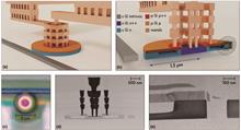
Convergence of high-performance silicon photonics and electronics, monolithically integrated in state-of-the-art CMOS platforms, is the holy grail for enabling the ultimate efficiencies, performance, and scaling of electronic-photonic systems-on-chip. It requires the emergence of platforms that combine state-of-the-art RF transistors with optimized silicon photonics, and a generation of photonic device technology with ultralow energies, increased operating spectrum, and the elimination of power-hungry thermal tuning. In this paper, in a co-optimized monolithic electronics-photonics platform (GlobalFoundries 45CLO), we turn the metal-oxide-semiconductor (MOS) field-effect transistor’s basic structure into a novel, highly efficient MOS capacitor ring modulator. It has the smallest ring cavity (1.5 μm radius), largest corresponding spur-free free spectral range (FSR=8.5 THz), and record 30 GHz/V shift efficiency in the O-band among silicon modulators demonstrated to date. With 1Vpp RF drive, we show an open optical eye while electro-optically tuning the modulator to track over 400 pm (69 GHz) change in the laser wavelength (using 2.5VDC range). A 90 GHz maximum electro-optic resonance shift is demonstrated with under 40 nW of power, providing a strong nonthermal tuning mechanism in a CMOS photonics platform. The modulator has a separately optimized body layer but shares the gate device layer and the gate oxide with 45 nm transistors, while meeting all CMOS manufacturability design rules. This type of convergent evolution of electronics and photonics may be the future of platforms for high-performance systems-on-chip.
Photonics Research
  • Publication Date: Dec. 22, 2021
  • Vol. 10, Issue 1, A1 (2022)
Compact low-birefringence polarization beam splitter using vertical-dual-slot waveguides in silicon carbide integrated platforms
Xiaodong Shi, Jingjing Zhang, Weichen Fan, Yaoqin Lu, Nianhua Peng, Karsten Rottwitt, and Haiyan Ou
The polarization beam splitter is a key component for polarization manipulation in photonic integrated circuits, but it is challenging to design for low-refractive-index optical materials, due to the low birefringence of the waveguides. We propose what we believe is a novel compact vertical-dual-slot waveguide-based coupling scheme for silicon carbide, enabling efficient low-birefringence polarization splitting by extensively modulating the transverse-magnetic mode distribution. We numerically and experimentally demonstrate the device in the 4H-silicon-carbide-on-insulator integrated platform, with a small footprint of 2.2 &mu;m&times;15 &mu;m. The device, easy to fabricate via a single lithography process as other components on the chip, exhibits low insertion loss of <0.71 dB and <0.51 dB for the transverse-electric and transverse-magnetic polarized light, respectively, and polarization extinction ratio of >13 dB, over 80 nm wavelength range.
Photonics Research
  • Publication Date: Dec. 22, 2021
  • Vol. 10, Issue 1, A8 (2022)
Research Articles
Fiber Optics and Optical Communications
Slope-assisted Raman distributed optical fiber sensing
Jian Li, Xinxin Zhou, Yang Xu, Lijun Qiao, Jianzhong Zhang, and Mingjiang Zhang
Raman distributed optical fiber sensing is required to achieve accurate temperature measurements in a micro-scale area. In this study, we first analyze and demonstrate the pulse transmission feature in the temperature variation area and the superposition characteristics of Raman optical time-domain reflectometry (OTDR) signals by numerical simulation. The equations of superimposed Raman anti-Stokes scattered signals at different stages are presented, providing a theoretical basis for the positioning and physical quantity demodulation of whole optical fiber systems based on the OTDR principle. Moreover, we propose and experimentally demonstrate a slope-assisted sensing principle and scheme in a Raman distributed optical fiber system. To the best our knowledge, this is the first experimental demonstration of Raman distributed optical fiber sensing in a centimeter-level spatial measurement region.
Photonics Research
  • Publication Date: Dec. 21, 2021
  • Vol. 10, Issue 1, 205 (2022)
Imaging Systems, Microscopy, and Displays
Freeform OST-HMD system with large exit pupil diameter and vision correction capability
Dewen Cheng, Jiaxi Duan, Hailong Chen, He Wang, Danyang Li, Qiwei Wang, Qichao Hou, Tong Yang, Weihong Hou, Donghua Wang, Xiaoyu Chi, Bin Jiang, and Yongtian Wang
Compactness and light weight, large exit pupil diameter and distance, small distortion for virtual image, and see-through light paths are pivotal factors to achieve a better, wearable experience of optical see-through head-mounted displays (OST-HMDs). In addition, light efficiency of the virtual image light path is an important factor for heat dissipation in HMD devices. This paper presents a new type of OST-HMD optical system that includes three wedge-shaped freeform prisms and two symmetric lenses. Based on a 0.71 in. microdisplay, an OST-HMD prototype with a diagonal field of view (FOV) of 45.3°, an F-number (F/#) of 1.8, an exit pupil size of 12 mm×8 mm, and an eye relief of 18 mm is demonstrated. The maximum value of distortion of the final system is 0.6% and 0.4% for virtual image and see-through light path, respectively. The overall dimension of the optical system per eye is no larger than 30 mm (width)×40 mm (height)×14 mm (thickness), and the weight of the optical module including lenses, holder, and microdisplay is 12.8 g. The light efficiency of the virtual image light path is up to 50% higher than those of other OST-HMD optical solutions.
Photonics Research
  • Publication Date: Dec. 09, 2021
  • Vol. 10, Issue 1, 21 (2022)
Single-pixel imaging using physics enhanced deep learning
Fei Wang, Chenglong Wang, Chenjin Deng, Shensheng Han, and Guohai Situ
Single-pixel imaging (SPI) is a typical computational imaging modality that allows two- and three-dimensional image reconstruction from a one-dimensional bucket signal acquired under structured illumination. It is in particular of interest for imaging under low light conditions and in spectral regions where good cameras are unavailable. However, the resolution of the reconstructed image in SPI is strongly dependent on the number of measurements in the temporal domain. Data-driven deep learning has been proposed for high-quality image reconstruction from a undersampled bucket signal. But the generalization issue prohibits its practical application. Here we propose a physics-enhanced deep learning approach for SPI. By blending a physics-informed layer and a model-driven fine-tuning process, we show that the proposed approach is generalizable for image reconstruction. We implement the proposed method in an in-house SPI system and an outdoor single-pixel LiDAR system, and demonstrate that it outperforms some other widespread SPI algorithms in terms of both robustness and fidelity. The proposed method establishes a bridge between data-driven and model-driven algorithms, allowing one to impose both data and physics priors for inverse problem solvers in computational imaging, ranging from remote sensing to microscopy.
Photonics Research
  • Publication Date: Dec. 13, 2021
  • Vol. 10, Issue 1, 104 (2022)
Slide-free histological imaging by microscopy with ultraviolet surface excitation using speckle illumination
Ivy H. M. Wong, Yan Zhang, Zhenghui Chen, Lei Kang, and Terence T. W. Wong
Microscopy with ultraviolet surface excitation (MUSE) is a promising slide-free imaging technique to improve the time-consuming histopathology workflow. However, since the penetration depth of the excitation light is tissue dependent, the image contrast could be significantly degraded when the depth of field of the imaging system is shallower than the penetration depth. High-resolution cellular imaging normally comes with a shallow depth of field, which also restricts the tolerance of surface roughness in biological specimens. Here we propose the incorporation of MUSE with speckle illumination (termed MUSES), which can achieve sharp imaging on thick and rough specimens. Our experimental results demonstrate the potential of MUSES in providing histological images with ∼1 μm spatial resolution and improved contrast, within 10 minutes for a field of view of 1.7 mm×1.2 mm. With the extended depth of field feature, MUSES also relieves the constraint of tissue flatness. Furthermore, with a color transformation assisted by deep learning, a virtually stained histological image can be generated without manual tuning, improving the applicability of MUSES in clinical settings.
Photonics Research
  • Publication Date: Dec. 16, 2021
  • Vol. 10, Issue 1, 120 (2022)
Quantum dots assisted in vivo two-photon microscopy with NIR-II emission
Huwei Ni, Yalun Wang, Tao Tang, Wenbin Yu, Dongyu Li, Mubin He, Runze Chen, Mingxi Zhang, and Jun Qian
With the advantages of high resolution and deep penetration depth, two-photon excited NIR-II (900–1880 nm) fluorescence (2PF) microscopic bioimaging is promising. However, due to the lack of imaging systems and suitable probes, few such works, to our best knowledge, were demonstrated utilizing NIR-II excitation and NIR-II fluorescence simultaneously. Herein, we used aqueously dispersible PbS/CdS quantum dots with bright NIR-II fluorescence as the contrast agents. Under the excitation of a 1550 nm femtosecond (fs) laser, they emitted bright 2PF in the NIR-II region. Moreover, a 2PF lifetime imaging microscopic (2PFLIM) system was implemented, and in vivo 2PFLIM images of mouse brain blood vessels were obtained for the first time to our best knowledge. To improve imaging speed, an in vivo two-photon fluorescence microscopy (2PFM) system based on an InGaAs camera was implemented, and in vivo 2PFM images of QDs-stained mouse brain blood vessels were obtained.
Photonics Research
  • Publication Date: Dec. 21, 2021
  • Vol. 10, Issue 1, 189 (2022)
Lock-in incoherent differential phase contrast imaging
Chiara Bonati, Damien Loterie, Timothé Laforest, and Christophe Moser
We introduce a lock-in method to increase the phase contrast in incoherent differential phase contrast (DPC) imaging. This method improves the phase sensitivity by the analog removal of the background. The use of a smart pixel detector with in-pixel signal demodulation, paired with synchronized switching illumination, provides the basis of a bit-efficient approach to emulate a lock-in DPC. The experiments show an increased sensitivity by a factor of up to 8, as expected from theory, and a reduction of collected data by a factor of 70, for equivalent standard DPC measurements; single-shot sensitivity of 0.7 mrad at a frame rate of 1400 frames per second is demonstrated. This new approach may open the way for the use of incoherent phase microscopy in biological applications where extreme phase sensitivity and millisecond response time are required.
Photonics Research
  • Publication Date: Dec. 22, 2021
  • Vol. 10, Issue 1, 237 (2022)
Instrumentation and Measurements
Long range dynamic displacement: precision PGC with sub-nanometer resolution in an LWSM interferometer
Yisi Dong, Peng-Cheng Hu, Haijin Fu, Hongxing Yang, Ruitao Yang, and Jiubin Tan
We propose a precision phase-generated-carrier (PGC) demodulation method with sub-nanometer resolution that avoids nonlinear errors in a laser wavelength sinusoidal modulation fiber-optic interferometer for long range dynamic displacement sensing. Using orthogonal detection and an AC-DC component extraction scheme, the PGC carrier phase delay (CPD) and laser intensity modulation phase delay can be obtained simultaneously to eliminate the nonlinear error from accompanied optical intensity modulation and CPD. Further, to realize long range displacement sensing, PGC phase modulation depth (PMD), determined by the laser wavelength modulation amplitude and the working distance of the interferometer, is required to maintain an optimal value during measurement, including initial position and dynamic movement. By combining frequency sweeping interference and modified PGC-arctan demodulation to measure real-time working distance, adaptive PMD technology is realized based on proportion control. We construct a fiber-optic Michelson and SIOS commercial interferometer for comparison and perform experiments to verify the feasibility of the proposed method. Experimental results demonstrate that an interferometer with sub-nanometer resolution and nanometer precision over a large range of 400 mm can be realized.
Photonics Research
  • Publication Date: Dec. 13, 2021
  • Vol. 10, Issue 1, 59 (2022)
Integrated Optics
Ultralow-loss compact silicon photonic waveguide spirals and delay lines
Shihan Hong, Long Zhang, Yi Wang, Ming Zhang, Yiwei Xie, and Daoxin Dai
Low-loss and compact optical waveguides are key for realizing various photonic integrated circuits with long on-chip delay lines, such as tunable optical delay lines, optical coherence tomography, and optical gyroscopes. In this paper, a low-loss and compact silicon photonic waveguide spiral is proposed by introducing broadened Archimedean spiral waveguides with a tapered Euler S-bend. A 100-cm-long waveguide spiral is realized with a minimal bending radius as small as 10 μm by using a standard 220-nm-thick silicon-on-insulator foundry process, and the measured propagation loss is as low as 0.28 dB/cm. Furthermore, the present waveguide spirals are used to realize a 10-bit tunable optical delay line, which has a footprint as small as 2.2 mm×5.9 mm and a dynamic range of 5120 ps with a fine resolution of 10 ps.
Photonics Research
  • Publication Date: Dec. 09, 2021
  • Vol. 10, Issue 1, 1 (2022)
Four-channel CWDM device on a thin-film lithium niobate platform using an angled multimode interferometer structure
Gengxin Chen, Ziliang Ruan, Zong Wang, Pucheng Huang, Changjian Guo, Daoxin Dai, Kaixuan Chen, and Liu Liu
A compact and high-performance coarse wavelength-division multiplexing (CWDM) device is introduced with a footprint of 2.1 mm×0.02 mm using an angled multimode interferometer structure based on a thin-film lithium niobate (TFLN) platform. The demonstrated device built on a 400 nm thick x-cut TFLN shows ultra-low insertion losses of 0.72 dB. Measured 3 dB bandwidths are 12.1 nm for all channels, and cross talks from adjacent channels are better than 18 dB. Its peak wavelength positions comply with the CWDM standard with a channel spacing of 20 nm. The filter bandwidth of the proposed CWDM device can be tuned by adjusting the structural parameters. This demonstrated CWDM device will promote future realization of multi-channel and multi-wavelength transmitter chips on TFLN.
Photonics Research
  • Publication Date: Dec. 09, 2021
  • Vol. 10, Issue 1, 8 (2022)
Anti-parity-time symmetry enabled on-chip chiral polarizer | Spotlight on Optics
Yanxian Wei, Hailong Zhou, Yuntian Chen, Yunhong Ding, Jianji Dong, and Xinliang Zhang
Encircling an exceptional point (EP) in a parity-time (PT) symmetric system has shown great potential for chiral optical devices, such as chiral mode switching for symmetric and antisymmetric modes. However, to our best knowledge, chiral switching for polarization states has never been reported, although chiral polarization manipulation has significant applications in imaging, sensing, communication, etc. Here, inspired by the anti-PT symmetry, we demonstrate, for the first time to our best knowledge, an on-chip chiral polarizer by constructing a polarization-coupled anti-PT symmetric system. The transmission axes of the chiral polarizer are different for forward and backward propagation. A polarization extinction ratio of over 10 dB is achieved for both propagating directions. Moreover, a telecommunication experiment is performed to demonstrate the potential applications in polarization encoding signals. It provides a novel functionality for encircling-an-EP parametric evolution and offers a new approach for on-chip chiral polarization manipulation.
Photonics Research
  • Publication Date: Dec. 13, 2021
  • Vol. 10, Issue 1, 76 (2022)
Silicon mode-loop Mach-Zehnder modulator with L-shaped PN junction for 0.37 V·cm VπL high-efficiency modulation
Jiacheng Liu, Gangqiang Zhou, Jiangbing Du, Weihong Shen, Linjie Zhou, and Zuyuan He
Optical signaling without a high voltage driver for electric-optic modulation is in high demand to reduce power consumption, packaging complexity, and cost. In this work, we propose and experimentally demonstrate a silicon mode-loop Mach–Zehnder modulator (ML-MZM) with record-high modulation efficiency. We used a mode-loop structure to recycle light twice in the phase shifter. With an L-shaped PN junction, a comparably large overlap between the PN junction and optical modes of both TE0 and TE1 was achieved to lower the driving voltage or decrease the photonic device size. Proof-of-concept high-efficiency modulation with low VπL of 0.37 V·cm was obtained. Subvoltage Vπ can be realized with a millimeter’s length phase shifter by this scheme, which makes the realization of CMOS-compatible driverless modulation highly possible. 40 Gb/s signaling with a bit error rate below the 7% forward-error-correction threshold was then demonstrated with the fabricated ML-MZM, indicating great potential for high-speed optical communication.
Photonics Research
  • Publication Date: Dec. 21, 2021
  • Vol. 10, Issue 1, 214 (2022)
Silicon substrate-integrated hollow waveguide for miniaturized optical gas sensing
Shaonan Zheng, Hong Cai, Linfang Xu, Nanxi Li, Zhonghua Gu, Yao Zhang, Weiguo Chen, Yanyan Zhou, Qingxin Zhang, and Lennon Yao Ting Lee
Gas sensors have a wide variety of applications. Among various existing gas sensing technologies, optical gas sensors have outstanding advantages. The development of the Internet of Things and consumer electronics has put stringent requirements on miniaturized gas sensing technology. Here, we demonstrate a chip-scale silicon substrate-integrated hollow waveguide (Si-iHWG) to serve as an optical channel and gas cell in an optical gas sensor. It is fabricated through silicon wafer etching and wafer bonding. The Si-iHWG chip is further assembled with an off-chip light source and detector to build a fully functional compact nondispersive infrared (NDIR) CO2 sensor. The chip size is 10 mm×9 mm, and the dimension of the sensor excluding the microcontroller board is 50 mm×25 mm×16 mm. This chip solution with compactness, versatility, robustness, and low cost provides a cost-effective platform for miniaturized optical sensing applications ranging from air quality monitoring to consumer electronics.
Photonics Research
  • Publication Date: Dec. 24, 2021
  • Vol. 10, Issue 1, 261 (2022)
Interview
Nanophotonics and Photonic Crystals
Controllable optofluidic assembly of biological cells using an all-dielectric one-dimensional photonic crystal | Editors' Pick
Fengya Lu, Lei Gong, Yan Kuai, Xi Tang, Yifeng Xiang, Pei Wang, and Douguo Zhang
Opto-thermophoretic manipulation is emerging as an effective way for versatile trapping, guiding, and assembly of biological nanoparticles and cells. Here we report a new opto-thermophoretic tweezer based on an all-dielectric one-dimensional photonic crystal (1DPC) for reversible assembly of biological cells with a controllable center. To reveal its ability of long-range optofluidic manipulation, we demonstrate the reversible assembly of many yeast cells as well as E. coli cells that are dispersed in water solution. The 1DPC-based tweezer can also exert short-range optical gradient forces associated with focused Bloch surface waves excited on the 1DPC, which can optically trap single particles. By combining both the optical and thermophoretic manipulation, the optically trapped single polystyrene particle can work as a controllable origin of the reversible cellular assembly. Numerical simulations are performed to calculate the temperature distribution and convective flow velocity on the 1DPC, which are consistent with the experimental observations and theoretically confirm the long-range manipulations on the all-dielectric 1DPC platform. The opto-thermophoretic tweezers based on all-dielectric 1DPC endow the micromanipulation toolbox for potential applications in biomedical sciences.
Photonics Research
  • Publication Date: Dec. 09, 2021
  • Vol. 10, Issue 1, 14 (2022)
Photonic topological transition in dimerized chains with the joint modulation of near-field and far-field couplings | Editors' Pick
Caifu Fan, Xi Shi, Feng Wu, Yunhui Li, Haitao Jiang, Yong Sun, and Hong Chen
Topological systems containing near-field or far-field couplings between unit cells have been widely investigated in quantum and classic systems. Their band structures are well explained with theories based on tight-binding or multiple scattering formalism. However, characteristics of the topology of the bulk bands based on the joint modulation of near-field and far-field couplings are rarely studied. Such hybrid systems are hardly realized in real systems and cannot be described by neither tight-binding nor multiple scattering theories. Here, we propose a hybrid-coupling photonic topological insulator based on a quasi-1D dimerized chain with the coexistence of near-field coupling within the unit cell and far-field coupling among all sites. Both theoretical and experimental results show that topological transition is realized by introducing near-field coupling for given far-field coupling conditions. In addition to closing and reopening the bandgap, the change in near-field coupling modulates the effective mass of photonics in the upper band from positive to negative, leading to an indirect bandgap, which cannot be achieved in conventional dimerized chains with either far-field or near-field coupling only.
Photonics Research
  • Publication Date: Dec. 09, 2021
  • Vol. 10, Issue 1, 41 (2022)
Mid-infrared quasi-BIC resonances with sub-wavelength slot mode profiles in germanium-based coupled guided-mode resonance structures | Editors' Pick
A. S. Lal Krishna, Sruti Menon, Asish Prosad, and Varun Raghunathan
We experimentally demonstrate a novel quasi-bound state in the continuum (BIC) resonance in the mid-infrared wavelength region with the resonant electric field confined as a slot mode within a low-refractive-index medium sandwiched between high-index layers. The structures studied here comprise coupled amorphous germanium guided-mode resonance (GMR) structures with a top one-dimensional grating layer and bottom uniform layer separated by a low-index silicon nitride layer. The slot-mode profile within the silicon nitride layer with mode field confinement >30% is achieved as a solution to the electromagnetic wave propagation through the coupled GMR structure with the dominant field component being perpendicular to the layers. The quasi-BIC resonance in symmetric 1D grating structures can be observed even at normal incidence when considering a realistic excitation beam with finite angular spread. The measured transmission peak is found to redshift (remain almost unchanged) under classical (full-conical) mounting conditions. The highest quality factor of ∼400 is experimentally extracted at normal incidence under a classical mounting condition with a resonance peak at 3.41 μm wavelength. Such slot-mode GMR structures with appropriately chosen low-index intermediate layers can find applications in resonantly enhanced sensing and active photonic devices.
Photonics Research
  • Publication Date: Dec. 13, 2021
  • Vol. 10, Issue 1, 68 (2022)
Experimental observation of multiple edge and corner states in photonic slabs heterostructures
Mingxing Li, Yueke Wang, Tian Sang, Hongchen Chu, Yun Lai, and Guofeng Yang
The photonic topological insulator has become an important research topic with a wide range of applications. Especially the higher-order topological insulator, which possesses gapped edge states and corner or hinge states in the gap, provides a new scheme for the control of light in a hierarchy of dimensions. In this paper, we propose a heterostructure composed of ordinary-topological-ordinary (OTO) photonic crystal slabs. Two coupled edge states (CESs) are generated due to the coupling between the topological edge states of the ordinary-topological interfaces, which opens up an effective way for high-capacity photonic transport. In addition, we obtain a new band gap between the CESs, and the two kinds of coupled corner states (CCSs) appear in the OTO bend structure. In addition, the topological corner state is also found, which arises from the filling anomaly of a lattice. Compared with the previous topological photonic crystal based on C-4 lattice, CESs, CCSs, and the topological corner state are all directly observed in experiment by using the near-field scanning technique, which makes the manipulation of the electromagnetic wave more flexible. We also verify that the three corner states are all robust to defects. Our work opens up a new way for guiding and trapping the light flow and provides a useful case for the coupling of topological photonic states.
Photonics Research
  • Publication Date: Dec. 21, 2021
  • Vol. 10, Issue 1, 197 (2022)
Nonlinear Optics
Enhanced optical nonlinearity in a silicon–organic hybrid slot waveguide for all-optical signal processing
Yonghua Wang, Su He, Xiaoyan Gao, Piaopiao Ye, Lei Lei, Wenchan Dong, Xinliang Zhang, and Ping Xu
Silicon photonic integrated devices used for nonlinear optical signal processing play a key role in ultrafast switching, computing, and modern optical communications. However, current devices suffer from limited operation speeds and low conversion efficiencies due to the intrinsically low nonlinear index of silicon. In this paper, we experimentally demonstrate enhanced optical nonlinearity in a silicon–organic hybrid slot waveguide consisting of an ultranarrow slot waveguide coated with a highly nonlinear organic material. The fabricated slot area is as narrow as 45 nm, which is, to the best of our knowledge, the narrowest slot width that has been experimentally reported in silicon slot waveguides. The nonlinear coefficient of the proposed device with a length of 3 mm is measured to be up to 1.43×10⁶ W-1 km-1. Based on the nanostructure design, the conversion efficiencies of degenerate four-wave mixing showed enhancements of more than 12 dB and 5 dB compared to those measured for an identical device without the organic material and a silicon strip waveguide, respectively. As a proof of concept, all-optical canonical logic units based on the prepared device with two inputs at 40 Gb/s are analyzed. The obtained logic results showed clear temporal waveforms and wide-open eye diagrams with error-free performance, illustrating that our device has great potential for use in high-speed all-optical signal processing and high-performance computing in the nodes and terminals of optical networks.
Photonics Research
  • Publication Date: Dec. 13, 2021
  • Vol. 10, Issue 1, 50 (2022)
Spatial cage solitons—taming light bullets
Chao Mei, Ihar Babushkin, Tamas Nagy, and Günter Steinmeyer
Multimode nonlinear optics is used to overcome a long-standing limitation of fiber optics, tightly phase locking several spatial modes and enabling the coherent transport of a wave packet through a multimode fiber. A similar problem is encountered in the temporal compression of multimillijoule pulses to few-cycle duration in hollow gas-filled fibers. Scaling the fiber length to up to 6 m, hollow fibers have recently reached 1 TW of peak power. Despite the remarkable utility of the hollow fiber compressor and its widespread application, however, no analytical model exists to enable insight into the scaling behavior of maximum compressibility and peak power. Here we extend a recently introduced formalism for describing mode locking to the analog scenario of locking spatial fiber modes together. Our formalism unveils the coexistence of two soliton branches for anomalous modal dispersion and indicates the formation of stable spatiotemporal light bullets that would be unstable in free space, similar to the temporal cage solitons in mode-locking theory. Our model enables deeper understanding of the physical processes behind the formation of such light bullets and predicts the existence of multimode solitons in a much wider range of fiber types than previously considered possible.
Photonics Research
  • Publication Date: Dec. 16, 2021
  • Vol. 10, Issue 1, 148 (2022)
Frequency upconversion detection of rotational Doppler effect
Haoxu Guo, Xiaodong Qiu, Song Qiu, Ling Hong, Fei Lin, Yuan Ren, and Lixiang Chen
We demonstrated an efficient scheme of measuring the angular velocity of a rotating object with the detection light working at the infrared regime. Our method benefits from the combination of second-harmonic generation (SHG) and rotational Doppler effect, i.e., frequency upconversion detection of rotational Doppler effect. In our experiment, we use one infrared light as the fundamental wave (FW) to probe the rotating objects while preparing the other FW to carry the desired superpositions of orbital angular momentum. Then these two FWs are mixed collinearly in a potassium titanyl phosphate crystal via type II phase matching, which produces the visible second-harmonic light wave. The experimental results show that both the angular velocity and geometric symmetry of rotating objects can be identified from the detected frequency-shift signals at the photon-count level. Our scheme will find potential applications in infrared monitoring.
Photonics Research
  • Publication Date: Dec. 21, 2021
  • Vol. 10, Issue 1, 183 (2022)
Single-scan polarization-resolved degenerate four-wave mixing spectroscopy using a vector optical field
Jiaqi Yuan, Xuemei Cheng, Xing Wang, Tengfei Jiao, and Zhaoyu Ren
We report on a new method to achieve the single-scan polarization-resolved degenerate four-wave mixing (DFWM) spectroscopy in a Rb atomic medium using a vector optical field, in which two pump beams are kept linearly polarized and a vector beam is employed as the probe beam. As the polarization and intensity of the DFWM signal are closely dependent on the polarization state of the probe beam, a vector probe beam with space-variant states of polarization is able to generate a DFWM signal with space-variant states of polarization and intensity across the DFWM image. Accordingly, the polarization-resolved spectra can be retrieved from a single DFWM image. To the best of our knowledge, this is the first time that the single-scan polarization-resolved spectrum detection has been realized experimentally with a vector beam. This work provides a simple but efficient single-scan polarization-resolved spectroscopic method, which would be of great utility for the samples of poor light stability and fast optical processes.
Photonics Research
  • Publication Date: Dec. 22, 2021
  • Vol. 10, Issue 1, 230 (2022)
Optical Devices
Ultrahigh detectivity, high-speed and low-dark current AlGaN solar-blind heterojunction field-effect phototransistors realized using dual-float-photogating effect
Kai Wang, Xinjia Qiu, Zesheng Lv, Zhiyuan Song, and Hao Jiang
High detectivity is essential for solar-blind deep-ultraviolet (DUV) light detection because the DUV signal is extremely weak in most applications. In this work, we report ultrahigh-detectivity AlGaN-based solar-blind heterojunction-field-effect phototransistors fabricated utilizing dual-float-photogating effect. The p+-Al0.4GaN layer and Al0.4GaN absorber layer deposited on the Al0.6GaN barrier serve as top pin-junction photogate, while the thin Al0.4GaN channel layer with a strong polarization field inside acts as virtual back photogate. Due to the effective depletion of the two-dimensional electron gas at the Al0.6Ga0.4N/Al0.4Ga0.6N heterointerface by the top photogate, the dark current was suppressed below 2 pA in the bias range of 0 to 10 V. A high photo-to-dark current ratio over 108 and an optical gain of 7.5×10⁴ were demonstrated at a bias of 5 V. Theoretical analysis indicates that the optical gain can be attributed to the joint action of the floating top and back photogates on the channel current. As a result, a record high flicker noise (Johnson and shot noise) limited specific detectivity of 2.84×10¹⁵(2.91×10¹⁷) cm Hz0.5 W-1 was obtained. Furthermore, high response speed at the microsecond level was also shown in the devices. This work provides a promising and feasible approach for high-sensitivity DUV detection.
Photonics Research
  • Publication Date: Dec. 13, 2021
  • Vol. 10, Issue 1, 111 (2022)
Efficient, high-CRI white LEDs by combining traditional phosphors with cadmium-free InP/ZnSe red quantum dots
Bega Karadza, Hannes Van Avermaet, Leila Mingabudinova, Zeger Hens, and Youri Meuret
Quantum dots (QDs) offer an interesting alternative for traditional phosphors in on-chip light-emitting diode (LED) configurations. Earlier studies showed that the spectral efficiency of white LEDs with high color rendering index (CRI) values could be considerably improved by replacing red-emitting nitride phosphors with narrowband QDs. However, the red QDs in these studies were cadmium-based, which is a restricted element in the EU and certain other countries. The use of InP-based QDs, the most promising Cd-free alternative, is often presented as an inferior solution because of the broader linewidth of these QDs. However, while narrow emission lines are the key to display applications that require a large color gamut, the spectral efficiency penalty of this broader emission is limited for lighting applications. Here, we report efficient, high-CRI white LEDs with an on-chip color converter coating based on red InP/ZnSe QDs and traditional green/yellow powder phosphors. Using InP/ZnSe QDs with a quantum yield of nearly 80% and a full width at half-maximum of 45 nm, we demonstrate high spectral efficiency for white LEDs with very high CRI values. One of the best experimental results in terms of both luminous efficacy and color rendering performance is a white LED with an efficacy of 132 lm/W, and color rendering indices of Ra≈90, R9≈50 for CCT ≈ 4000 K. These experimental results are critically compared with theoretical benchmark values for white LEDs with on-chip downconversion from both phosphors and red Cd-based QDs. The various loss mechanisms in the investigated white LEDs are quantified with an accurate simulation model, and the main impediments to an even higher efficacy are identified as the blue LED wall-plug efficiency and light recycling in the LED package.
Photonics Research
  • Publication Date: Dec. 16, 2021
  • Vol. 10, Issue 1, 155 (2022)
Optoelectronics
Near-infrared electroluminescence of AlGaN capped InGaN quantum dots formed by controlled growth on photoelectrochemical etched quantum dot templates
Xiongliang Wei, Syed Ahmed Al Muyeed, Haotian Xue, Elia Palmese, Renbo Song, Nelson Tansu, and Jonathan J. Wierer
Near-infrared electroluminescence of InGaN quantum dots (QDs) formed by controlled growth on photoelectrochemical (PEC) etched QD templates is demonstrated. The QD template consists of PEC InGaN QDs with high density and controlled sizes, an AlGaN capping layer to protect the QDs, and a GaN barrier layer to planarize the surface. Scanning transmission electron microscopy (STEM) of Stranski–Krastanov (SK) growth on the QD template shows high-In-content InGaN QDs that align vertically to the PEC QDs due to localized strain. A high-Al-content Al0.9Ga0.1N capping layer prevents the collapse of the SK QDs due to intermixing or decomposition during higher temperature GaN growth as verified by STEM. Growth of low-temperature (830°C) p-type layers is used to complete the p-n junction and further ensure QD integrity. Finally, electroluminescence shows a significant wavelength shift (800 nm to 500 nm), caused by the SK QDs’ tall height, high In content, and strong polarization-induced electric fields.
Photonics Research
  • Publication Date: Dec. 09, 2021
  • Vol. 10, Issue 1, 33 (2022)
Comb-based photonic neural population for parallel and nonlinear processing
Bowen Ma, Junfeng Zhang, and Weiwen Zou
It is believed that neural information representation and processing relies on the neural population instead of a single neuron. In neuromorphic photonics, photonic neurons in the form of nonlinear responses have been extensively studied in single devices and temporal nodes. However, to construct a photonic neural population (PNP), the process of scaling up and massive interconnections remain challenging considering the physical complexity and response latency. Here, we propose a comb-based PNP interconnected by carrier coupling with superior scalability. Two unique properties of neural population are theoretically and experimentally demonstrated in the comb-based PNP, including nonlinear response curves and population activities coding. A classification task of three input patterns with dual radio-frequency (RF) tones is successfully implemented in a time-efficient manner, which allows the comb-based PNP to make effective use of the ultra-broad bandwidth of photonics for parallel and nonlinear processing.
Photonics Research
  • Publication Date: Dec. 21, 2021
  • Vol. 10, Issue 1, 174 (2022)
Silicon Photonics
Electrically injected GeSn lasers with peak wavelength up to 2.7 μm | On the Cover
Yiyin Zhou, Solomon Ojo, Chen-Wei Wu, Yuanhao Miao, Huong Tran, Joshua M. Grant, Grey Abernathy, Sylvester Amoah, Jake Bass, Gregory Salamo, Wei Du, Guo-En Chang, Jifeng Liu, Joe Margetis, John Tolle, Yong-Hang Zhang, Greg Sun, Richard A. Soref, Baohua Li, and Shui-Qing Yu
GeSn lasers enable the monolithic integration of lasers on the Si platform using all-group-IV direct-bandgap material. The GeSn laser study recently moved from optical pumping into electrical injection. In this work, we present explorative investigations of GeSn heterostructure laser diodes with various layer thicknesses and material compositions. Cap layer material was studied by using Si0.03Ge0.89Sn0.08 and Ge0.95Sn0.05, and cap layer total thickness was also compared. The 190 nm SiGeSn-cap device had threshold of 0.6 kA/cm2 at 10 K and a maximum operating temperature (Tmax) of 100 K, compared to 1.4 kA/cm2 and 50 K from 150 nm SiGeSn-cap device, respectively. Furthermore, the 220 nm GeSn-cap device had 10 K threshold at 2.4 kA/cm2 and Tmax at 90 K, i.e., higher threshold and lower maximal operation temperature compared to the SiGeSn cap layer, indicating that enhanced electron confinement using SiGeSn can reduce the threshold considerably. The study of the active region material showed that device gain region using Ge0.87Sn0.13 had a higher threshold and lower Tmax, compared to Ge0.89Sn0.11. The performance was affected by the metal absorption, free carrier absorption, and possibly defect density level. The maximum peak wavelength was measured as 2682 nm at 90 K by using Ge0.87Sn0.13 in gain regions. The investigations provide directions to the future GeSn laser diode designs toward the full integration of group-IV photonics on a Si platform.
Photonics Research
  • Publication Date: Dec. 21, 2021
  • Vol. 10, Issue 1, 222 (2022)
Metasurface doublet-integrated bidirectional grating antenna enabling enhanced wavelength-tuned beam steering
Woo-Bin Lee, Chul-Soon Im, Changyi Zhou, Bishal Bhandari, Duk-Yong Choi, and Sang-Shin Lee
We propose and demonstrate an optical phased-array-based bidirectional grating antenna (BDGA) in silicon nitride waveguides. The BDGA is integrated with a miniaturized all-dielectric metasurface doublet (MD) formed on a glass substrate. The BDGA device, which takes advantage of alternately feeding light to its ports in opposite directions, is presumed to effectively provide a doubled wavelength-tuned steering efficiency compared to its unidirectional counterpart. The MD, which is based on vertically cascaded convex and concave metalenses comprising circular hydrogenated amorphous silicon nanopillars, is meticulously placed atop the BDGA chip to accept and deflect a beam emanating from the emission area, thereby boosting the beam-steering performance. The manufactured BDGA could achieve an enhanced beam-steering efficiency of 0.148 deg/nm as well as a stable spectral emission response in the wavelength range of 1530–1600 nm. By deploying a fabricated MD atop the silicon photonic BDGA chip, the steering efficiency was confirmed to be boosted by a factor of ∼3.1, reaching 0.461 deg/nm, as intended.
Photonics Research
  • Publication Date: Dec. 22, 2021
  • Vol. 10, Issue 1, 248 (2022)
Surface Optics and Plasmonics
Highly sensitive plasmonic nanorod hyperbolic metamaterial biosensor
Ruoqin Yan, Tao Wang, Xinzhao Yue, Huimin Wang, Yu-Hui Zhang, Peng Xu, Lu Wang, Yuandong Wang, and Jinyan Zhang
Plasmonic sensing based on nanostructures is a powerful analytical tool for ultrasensitive label-free biomolecule detection that holds great potential in the field of clinical diagnostics and biomedical research. Here, we report the fabrication, the characterization, and the principle of operation of gold nanorod hyperbolic metamaterials (NHMMs) along with ultrasensitive bulk refractive index and label-free biomolecular detection. By combining electron-beam lithography and nanoscale electroplating, we demonstrate the fabrication of a highly ordered, height-controllable, and vertical array of nanorods. By exciting the bulk plasmon–polariton mode in the NHMM using a prism-coupling technique and integrating the sensor in microfluidics, we demonstrate that the bulk sensitivity and figure of merit of our device could reach 41,600 nm/RIU and 416 RIU-1, respectively. The physical mechanism of this high bulk sensitivity is revealed through theoretical and experimental studies. Moreover, by bio-functionalizing the surface of the NHMM sensor, monitoring the binding of streptavidin at dilute concentrations is performed in real time. We test different concentrations of streptavidin ranging from 200 to 5 µg/mL, and the NHMM biosensor exhibits a 1 nm wavelength shift for a 5 µg/mL streptavidin detection. By fitting the Hill equation of the NHMM biosensor and taking into account the level of noise (0.05 nm) as the minimum wavelength shift of the detectable limit, the limit of detection of the NHMM biosensor to streptavidin can be estimated to be 0.14 µg/mL (2.4 nm). As a direct comparison, a 0.5 nm wavelength shift for 20 µg/mL of streptavidin is reported when using a conventional gold film sensor under identical experimental conditions. The developed plasmonic NHMM sensor shows tremendous potential for highly sensitive bulk solutions and biomolecule detection and provides a promising avenue for free-label biosensing applications in the future.
Photonics Research
  • Publication Date: Dec. 13, 2021
  • Vol. 10, Issue 1, 84 (2022)
Performance improvement approaches for optical fiber SPR sensors and their sensing applications
Jianying Jing, Kun Liu, Junfeng Jiang, Tianhua Xu, Shuang Wang, Jinying Ma, Zhao Zhang, Wenlin Zhang, and Tiegen Liu
Optical fiber surface plasmon resonance (SPR) sensors point toward promising application potential in the fields of biomarker detection, food allergen screening, and environmental monitoring due to their unique advantages. This review outlines approaches in improving the fiber SPR sensing performance, e.g., sensitivity, detection accuracy, reliability, cross-sensitivity, selectivity, convenience and efficiency, and corresponding sensing applications. The sensing principles of SPR sensors, especially the performance indicators and their influencing factors, have been introduced. Current technologies for improving the fiber SPR performance and their application scenarios are then reviewed from the aspects of fiber substrate, intrinsic layer (metal layer), and surface nanomaterial modification. Reasonable design of the substrate can strengthen the evanescent electromagnetic field and realize the multi-parameter sensing, and can introduce the in situ sensing self-compensation, which allows corrections for errors induced by temperature fluctuation, non-specific binding, and external disturbances. The change of the intrinsic layer can adjust the column number, the penetration depth, and the propagation distance of surface plasmon polaritons. This can thereby promote the capability of sensors to detect the large-size analytes and can reduce the full width at half-maximum of SPR curves. The modification of various-dimensionality nanomaterials on the sensor surfaces can heighten the overlap integral of the electromagnetic field intensity in the analyte region and can strengthen interactions between plasmons and excitons as well as interactions between analyte molecules and metal surfaces. Moreover, future directions of fiber SPR sensors are prospected based on the important and challenging problems in the development of fiber SPR sensors.
Photonics Research
  • Publication Date: Dec. 16, 2021
  • Vol. 10, Issue 1, 126 (2022)
Single-particle trapping and dynamic manipulation with holographic optical surface-wave tweezers
Xi Xie, Xianyou Wang, Changjun Min, Haixiang Ma, Yunqi Yuan, Zhangyu Zhou, Yuquan Zhang, Jing Bu, and Xiaocong Yuan
Optical surface waves have widely been used in optical tweezers systems for trapping particles sized from the nano- to microscale, with specific importance and needs in applications of super-resolved detection and imaging if a single particle can be trapped and manipulated accurately. However, it is difficult to achieve such trapping with high precision in conventional optical surface-wave tweezers. Here, we propose and experimentally demonstrate a new method to accurately trap and dynamically manipulate a single particle or a desired number of particles in holographic optical surface-wave tweezers. By tailoring the optical potential wells formed by surface waves, we achieved trapping of the targeted single particle while pushing away all surrounding particles and further dynamically controlling the particle by a holographic tweezers beam. We also prove that different particle samples, including gold particles and biological cells, can be applied in our system. This method can be used for different-type optical surface-wave tweezers, with significant potential applications in single-particle spectroscopy, particle sorting, nano-assembly, and others.
Photonics Research
  • Publication Date: Dec. 16, 2021
  • Vol. 10, Issue 1, 166 (2022)
Ultrafast Optics
Active stabilization of terahertz waveforms radiated from a two-color air plasma
Yonghao Mi, Kyle Johnston, Valentina Shumakova, Søren H. Møller, Kamalesh Jana, Chunmei Zhang, André Staudte, Shawn Sederberg, and Paul B. Corkum
Intense laser fields focused into ambient air can be used to generate high-bandwidth current densities in the form of plasma channels and filaments. Excitation with bichromatic fields enables us to adjust the amplitude and sign of these currents using the relative phase between the two light pulses. Two-color filamentation in gas targets provides a route to scaling the energy of terahertz pulses to microjoule levels by driving the plasma channel with a high-energy laser source. However, the structure of plasma channels is highly susceptible to drifts in both the relative phase and other laser parameters, making control over the waveform of the radiated terahertz fields delicate. We establish a clear link between the phase dependence of plasma currents and terahertz radiation by comparing in situ detection of current densities and far-field detection of terahertz electric fields. We show that the current measurement can be used as a feedback parameter for stabilizing the terahertz waveform. This approach provides a route to energetic terahertz pulses with exceptional waveform stability.
Photonics Research
  • Publication Date: Dec. 13, 2021
  • Vol. 10, Issue 1, 96 (2022)

About the Cover

The GeSn double heterostructure laser diode generates the laser beam. With the GeSn active region, this laser is composited by the all-group-IV semiconductor and alloy (namely Si, Ge, GeSn, and SiGeSn), enabling the monolithic integration of lasers on the Si platform.