
Kai Wang, Xinjia Qiu, Zesheng Lv, Zhiyuan Song, Hao Jiang, "Ultrahigh detectivity, high-speed and low-dark current AlGaN solar-blind heterojunction field-effect phototransistors realized using dual-float-photogating effect," Photonics Res. 10, 111 (2022)
- Photonics Research
- Vol. 10, Issue 1, 111 (2022)
Abstract
1. INTRODUCTION
Recent progress in preparing ultrawide-bandgap semiconductors has greatly promoted the research of solid-state ultraviolet detection, especially the solar-blind photodetection inside the deep-ultraviolet (DUV) band (wavelength of
AlGaN is one of the most promising materials for solar-blind DUV detection because of its tunable direct bandgap corresponding to the DUV spectral region and its advances in epitaxial growth and processing technologies. AlGaN-based heterojunctions with high-density two-dimensional electron gas (2DEG) at the heterojunction interface have been successfully used not only in high electron mobility transistors [4] but also for high-responsivity UV photodetectors [5,6]. Benefiting from the high conductivity of 2DEG channel, AlGaN-based UV heterojunction field effect phototransistors (HFEPTs) can generally exhibit an ultrahigh photoconductive gain and the resulting high responsivity. Although the photoconductive gain of AlGaN HFEPT can match or even exceed the optical gain of the typical gain-type photodetectors, such as avalanche photodiodes [7,8] and heterojunction phototransistors [9,10], the conductivity of 2DEG channel also leads to high dark current, which reduces the detectivity [11,12].
One solution is to deposit a
Sign up for Photonics Research TOC. Get the latest issue of Photonics Research delivered right to you!Sign up now
In addition to the barrier side of the AlGaN heterojunction, the conductivity modulation of 2DEG channel by the photovoltage may also be achieved from the channel layer side. It is expected to further improve the performance characteristics of AlGaN solar-blind HFEPT by introducing the photovoltage effect into the channel layer via manipulating the strain-induced polarization field.
In this work,
2. EXPERIMENTAL SECTION
Samples used in this work were grown on c-plane sapphire substrates by metal-organic chemical vapor deposition (MOCVD) in a low-pressure reactor. The epilayers, from bottom to top, consist of a 500 nm thick AlN buffer layer deposited at 1080°C, a 160 nm thick unintentionally doped (uid)
Device fabrication was started with
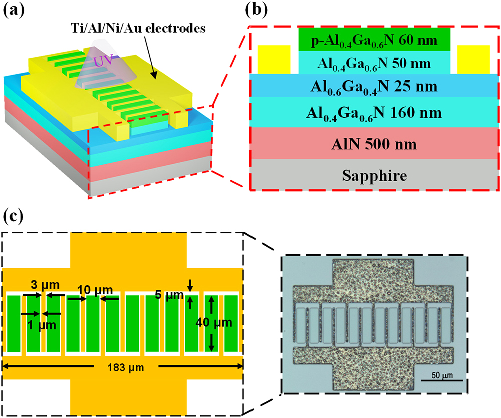
Figure 1.(a) Schematic illustration of the PG-HFEPT and (b) its cross-sectional view. (c) Schematic diagram and optical image of the interdigitated electrodes, mentioning the device dimensions.
Transmittance and reflection spectra of the deposited epilayers grown on double-side polished (0001) sapphire substrates were recorded using a Shimadzu UV2550 ultraviolet-visible spectrophotometer. X-ray diffraction (XRD) reciprocal space mapping (RSM) was applied to characterize the epitaxial structure. The RSM measurements were carried out using a high-resolution XRD instrument (Bruker D8 DISCOVERY). Current-voltage (I-V) characteristics of the fabricated devices were analyzed using a Keithley 4200-SCS semiconductor parameter analyzer under dark and DUV-illuminated conditions. The fabricated photodetectors were illuminated from the top side and the incident light source was a deep-UV light-emitting diode with a peak wavelength of 260 nm. Spectral responses were measured in the 200 to 400 nm wavelength range under the different bias voltages at room temperature using a xenon/deuterium lamp and a monochromator with 1200 g/mm grating as the light source. A Newport power meter was used to determine the incident power densities over the measuring range. Time-dependent photoresponse was measured by modulating the output light from the monochromator using an electronic shutter with a timing resolution of 1 ms. In the measurement, the modulation period of the light source is 60 s, including 30 s on time and 30 s off time. The transient response of the fabricated devices was investigated using a high-speed oscilloscope (6 GHz, Keysight DSOS604A) excited by a 260 nm UV laser with pulse width of 625 ps and repetition frequency of 1 kHz. Noise spectra were collected by an FS-Pro multifunctional semiconductor parameter tester.
3. RESULTS AND DISCUSSION
The optical and structural properties of the epitaxial sample were at first characterized. It can be seen from the transmission spectrum that the absorption edge of
![]()
Figure 2.(a) Transmission and reflection spectra of the epitaxial structure with p-type photogate. (b) XRD RSM for the epitaxial structure taken around (105) reflection, in which the dashed lines correspond to fully strained (
Considering the effects of spontaneous and piezoelectric polarization, the energy band diagrams of the epitaxial samples with and without
Figures 3(a) and 3(b) compare the I-V characteristics of the two-terminal PG-HFEPT and HFEPT measured in dark and DUV illuminated conditions. For the PG-HFEPT, the dark current (
![]()
Figure 3.Dark and illuminated
The optical gain can be estimated from
To illustrate the high gain mechanism of the PG-HFEPT, we analyze the factors contributing to the
![]()
Figure 4.(a) Schematic diagram of the photogenerated carriers and their movement in the absorber, barrier, and channel layers of PG-HFEPT. Schematic band diagrams of (b) the top p-type photogate heterojunction and (c) the virtual back-photogate heterojunction together with the barrier layer outside the p-photogate under dark and illumination conditions.
In the channel layer region, the photogenerated electrons also drift into the 2DEG channel by the built-in field (downward bending of the band) pointing to the substrate. In contrast, the photogenerated holes move toward the uid-
In addition, for the barrier layer region exposed to the surface, the strong polarization field in this region may move the photogenerated holes towards the surface and neutralize the trapped surface electrons, resulting in a positive virtual gate bias and a consequent increase of the channel photocurrent. However, in the PG-HFEPT, the contribution from this part can be considered negligible. From the peak absorption coefficient at the absorption edge [21] and the proportion in the total effective detection area, it can be estimated that only less than 10% of the absorbable incident DUV light is absorbed in the 25 nm thick
Based on the above factors, the total change of the channel photocurrent can be regarded as the sum of the photocurrent increased under the action of the top p-type photogate and the virtual back photogate, i.e.,
Using the above equations, the theoretical
To further assess the performance of the PG-HFEPT, we investigate the incident power dependency of the photoresponse. Figure 5(a) gives the
![]()
Figure 5.(a)
One of the most important specifications of photodetector is the detectivity. Normalized signal-to-noise performance of a photodetector is usually described by specific detectivity
If the shot noise from the dark current is the dominant contribution, the specific detectivity can be calculated by
The detectivity
A more accurate evaluation of detectivity, however, is to take into account the flicker noise at low frequency. Accordingly, the noise power spectra were measured from the two HFEPTs in the frequency range of 1 Hz to 100 kHz at bias voltages of 1 and 5 V as shown in Fig. 6(a). Compared with the HFEPT, the noise power density of the PG-HFEPT is more than 3 orders of magnitude lower, and the dispersion of the spectral density is smaller under different bias voltages. The measured noise power spectrum is described by
![]()
Figure 6.(a) Noise power density spectra of the PG-HFEPT and HFEPT measured at different biases. (b) Impulse response of the two phototransistors measured at 3 V bias. The inset is the time-dependent photoresponse of the two phototransistors at 3 V bias measured at 260 nm irradiation with a 30 s on/off cycle.
The transient responses of the phototransistors were also characterized. In the measurements, the pulse width of the 260 nm light was 625 ps, and the repetition rate was 1 kHz. Figure 6(b) gives the impulse responses measured at a bias of 3 V. The rise (
The much longer
Shown in the inset of Fig. 6(b) are the time-dependent photoresponses of the two phototransistors at 3 V bias measured by periodically turning on and off the 260 nm incident light. The responses are given in the form of on/off current ratio to more clearly show the difference between the responses of the two devices. Both phototransistors showed good stability and reproducibility to the periodic 260 nm irradiation. Benefiting from the low dark current, the PG-HFEPTs demonstrate an on/off current ratio of 2 orders of magnitude higher than HFEPT.
To better understand the performance level of our device, Table 1 compares the main characteristic parameters of our PG-HFEPT with those of the representative solar blind UV photodetectors reported previously. It is shown that the solar-blind PG-HFEPTs have a record high specific detectivity. Moreover, the
Comparison of Characteristic Parameters of Our Detectors Using Dual-Photogating Effects to Those of Published Solar-Blind UV Photodetectors
| Material | Type | Refs. | ||||
|---|---|---|---|---|---|---|
| AlGaN | HFEPT | 0.0044/0.591 | This work | |||
| Heterojunction | 0.053 ( | — | 200/200 | [ | ||
| Heterojunction | 0.0023 (0 V) | 37/45 | [ | |||
| MSM | 46 (20 V) | 0.0009/0.0119 | [ | |||
| AlGaN | MSM | 3.63 (5 V) | — | 1130/133 | [ | |
| AlGaN | p-i-n | 0.131 (5 V) | 140/8200 | [ | ||
| AlGaN/GaN | Schottky | 0.09 (50 V) | — | — | [ | |
| AlGaN | p-i-n | 0.09 (5 V) | — | — | [ | |
| AlGaN | APD | 0.13 (20 V) | — | [ |
Johnson and shot noise limited
Shot noise limited
Johnson noise limited
4. CONCLUSIONS
In conclusion, solar-blind AlGaN HFEPTs utilizing dual-float-photogating effect have been reported. The fabricated devices with an interdigital configuration exhibit a very low dark current of less than 2 pA in the bias range of 0 to 10 V, due to the effective depletion of the 2DEG channel by the
References
[1] C. Xie, X. T. Lu, X. W. Tong, Z. X. Zhang, F. X. Liang, L. Liang, L. B. Luo, Y. C. Wu. Recent progress in solar-blind deep-ultraviolet photodetectors based on inorganic ultrawide bandgap semiconductors. Adv. Funct. Mater., 29, 1806006(2019).
[2] M. Razeghi. Short-wavelength solar-blind detectors: status, prospects, and markets. Proc. IEEE, 90, 1006-1014(2002).
[3] G. Chen, F. Abou-Galala, Z. Xu, B. M. Sadler. Experimental evaluation of LED-based solar blind NLOS communication links. Opt. Express, 16, 15059-15068(2008).
[4] Y. F. Wu, D. Kapolnek, J. P. Ibbetson, P. Parikh, B. P. Keller, U. K. Mishra. Very-high power density AlGaN/GaN HEMTs. IEEE Trans. Electron Devices, 48, 2181-2183(2001).
[5] T.-M. Kuan, S.-J. Chang, Y.-K. Su, C.-H. Ko, J. B. Webb, J. A. Bardwell, Y. Liu, H. Tang, W.-P. Lin, Y.-T. Cherng, W.-H. Lan. High optical-gain AlGaN/GaN2 dimensional electron gas photodetectors. Jpn. J. Appl. Phys., 42, 5563-5564(2003).
[6] A. Yoshikawa, S. Ushida, K. Nagase, M. Iwaya, T. Takeuchi, S. Kamiyama, I. Akasaki. High-performance solar-blind Al0.6Ga0.4N/Al0.5Ga0.5N MSM type photodetector. Appl. Phys. Lett., 111, 191103(2017).
[7] H. L. Wu, W. C. Wu, H. X. Zhang, Y. D. Chen, Z. S. Wu, G. Wang, H. Jiang. All AlGaN epitaxial structure solar-blind avalanche photodiodes with high efficiency and high gain. Appl. Phys. Express, 9, 052103(2016).
[8] Z. G. Shao, D. J. Chen, H. Lu, R. Zhang, D. P. Cao, W. J. Luo, Y. D. Zheng, L. Li, Z. H. Li. High-gain AlGaN solar-blind avalanche photodiodes. IEEE Electron Device Lett., 35, 372-374(2014).
[9] L. X. Zhang, S. J. Tang, C. S. Liu, B. Li, H. L. Wu, H. L. Wang, Z. S. Wu, H. Jiang. Demonstration of solar-blind Al
[10] L. J. Sun, Z. S. Lv, Z. H. Zhang, X. J. Qiu, H. Jiang. High-performance AlGaN heterojunction phototransistor with dopant-free polarization-doped p-base. IEEE Electron Device Lett., 41, 325-328(2020).
[11] T. Narita, A. Wakejima, T. Egawa. Ultraviolet photodetectors using transparent gate AlGaN/GaN high electron mobility transistor on silicon substrate. Jpn. J. Appl. Phys., 52, 01AG06(2013).
[12] A. M. Armstrong, B. Klein, A. A. Allerman, E. A. Douglas, A. G. Baca, M. H. Crawford, G. W. Pickrell, C. A. Sanchez. Visible-blind and solar-blind detection induced by defects in AlGaN high electron mobility transistors. J. Appl. Phys., 123, 114502(2018).
[13] Q. F. Lyu, H. X. Jiang, K. M. Lau. High gain and high ultraviolet/visible rejection ratio photodetectors using p-GaN/AlGaN/GaN heterostructures grown on Si. Appl. Phys. Lett., 117, 071101(2020).
[14] M. Iwaya, S. Miura, T. Fujii, S. Kamiyama, H. Amano, I. Akasaki. High-performance UV detector based on AlGaN/GaN junction heterostructure-field-effect transistor with a p-GaN gate. Phys. Status Solidi C, 6, S972-S975(2009).
[15] M. A. Khan, Q. Chen, J. N. Kuznia, C. J. Sun, M. S. Shur. Gated photodetector based on GaN/AlGaN heterostructure field effect transistor. Electron. Lett., 31, 398-400(1995).
[16] S. H. Baek, G. W. Lee, C. Y. Cho, S. N. Lee. Gate-controlled amplifiable ultraviolet AlGaN/GaN high-electron-mobility phototransistor. Sci. Rep., 11, 7172(2021).
[17] X. J. Qiu, H. Jiang. Highly conductive and 260 nm transparent p-type Al0.6Ga0.4N achieved utilizing interface doping effects. Cryst. Growth Des., 21, 2389-2397(2021).
[18] H. Jiang, G. Y. Zhao, H. Ishikawa, T. Egawa, T. Jimbo, M. Umeno. Determination of exciton transition energy and bowing parameter of AlGaN alloys in AlGaN/GaN heterostructure by means of reflectance measurement. J. Appl. Phys., 89, 1046-1052(2001).
[19] P. Cantu, F. Wu, P. Waltereit, S. Keller, A. E. Romanov, S. P. DenBaars, J. S. Speck. Role of inclined threading dislocations in stress relaxation in mismatched layers. J. Appl. Phys., 97, 103534(2005).
[20] A. Jiménez, Z. Bougrioua, J. M. Tirado, A. F. Braña, E. Calleja, E. Muñoz, I. Moerman. Improved AlGaN/GaN high electron mobility transistor using AlN interlayers. Appl. Phys. Lett., 82, 4827-4829(2003).
[21] K. Takeuchi, S. Adachi, K. Ohtsuka. Optical properties of Al
[22] Z. H. Zaidi, P. A. Houston. Highly sensitive UV detection mechanism in AlGaN/GaN HEMTs. IEEE Trans. Electron Devices, 60, 2776-2781(2013).
[23] M. A. Green. Solar cells—operating principles, technology and system applications. Sol. Energy, 28, 447(1982).
[24] S. M. Sze, K. K. Ng. Physics of Semiconductor Devices(2006).
[25] B. Chen, W. Y. Jiang, J. Yuan, A. L. Holmes, B. M. Onat. Demonstration of a room-temperature InP-based photodetector operating beyond 3 μm. IEEE Photon. Technol. Lett., 23, 218-220(2011).
[26] H. Bae, A. Charnas, X. Sun, J. Noh, M. Si, W. Chung, G. Qiu, X. Lyu, S. Alghamdi, H. Wang, D. Zemlyanov, P. D. Ye. Solar-blind UV photodetector based on atomic layer-deposited Cu2O and nanomembrane β-Ga2O3 pn oxide heterojunction. ACS Omega, 4, 20756-20761(2019).
[27] J. Ma, X. Xia, S. Yan, Y. Li, W. Liang, J. Yan, X. Chen, D. Wu, X. Li, Z. Shi. Stable and self-powered solar-blind ultraviolet photodetectors based on a Cs3Cu2I5/β-Ga2O3 heterojunction prepared by dual-source vapor codeposition. ACS Appl. Mater. Interfaces, 13, 15409-15419(2021).
[28] B. S. Qiao, Z. Z. Zhang, X. H. Xie, B. H. Li, K. X. Li, X. Chen, H. F. Zhao, K. W. Liu, L. Liu, D. Z. Shen. Avalanche gain in metal-semiconductor-metal Ga2O3 solar-blind photodiodes. J. Phys. Chem. C, 123, 18516-18520(2019).
[29] S. C. Wu, M. J. Wu, Y. F. Chen. Nanolayered graphene/hexagonal boron nitride/n-AlGaN heterostructures as solar-blind deep-ultraviolet photodetectors. ACS Appl. Nano Mater., 3, 7595-7603(2020).
[30] J. Z. Li, J. Y. Lin, H. X. Jiang, M. A. Khan, Q. Chen. Persistent photoconductivity in a two-dimensional electron gas system formed by an AlGaN/GaN heterostructure. J. Appl. Phys., 82, 1227-1230(1997).
[31] J. Sun, T. Zhan, Z. Liu, J. Wang, X. Yi, P. M. Sarro, G. Zhang. Suppression of persistent photoconductivity AlGaN/GaN heterostructure photodetectors using pulsed heating. Appl. Phys. Express, 12, 122007(2019).
[32] A. Kalra, S. Rathkanthiwar, R. Muralidharan, S. Raghavan, D. N. Nath. Material-to-device performance correlation for AlGaN-based solar-blind p-i-n photodiodes. Semicond. Sci. Technol., 35, 035001(2020).
[33] N. Biyikli, O. Aytur, I. Kimukin, T. Tut, E. Ozbay. Solar-blind AlGaN-based Schottky photodiodes with low noise and high detectivity. Appl. Phys. Lett., 81, 3272-3274(2002).
[34] C. J. Collins, U. Chowdhury, M. M. Wong, B. Yang, A. L. Beck, R. D. Dupuis, J. C. Campbell. Improved solar-blind detectivity using an Al
[35] T. Tut, M. Gokkavas, A. Inal, E. Ozbay. Al


Set citation alerts for the article
Please enter your email address

© Copyright 2018-2021 | Chinese Laser Press. All Rights Reserved 沪ICP备15018463号-20