
Yonghua Wang, Su He, Xiaoyan Gao, Piaopiao Ye, Lei Lei, Wenchan Dong, Xinliang Zhang, Ping Xu, "Enhanced optical nonlinearity in a silicon–organic hybrid slot waveguide for all-optical signal processing," Photonics Res. 10, 50 (2022)
- Photonics Research
- Vol. 10, Issue 1, 50 (2022)
Abstract
1. INTRODUCTION
Optical nonlinearities are indispensable for all-optical signal processing in fast computing and communication applications [1,2]. In these application cases, the nonlinearities are not suppressed as in optical transmission applications, but instead, they are utilized, and it is therefore desirable to make highly nonlinear devices. All-optical signal processing has been studied in various highly nonlinear media that leverage different nonlinear processes, such as highly nonlinear optical fibers [3–5], optical semiconductor amplifiers [6], and periodically poled lithium niobate devices [7,8]. Among these nonlinear devices, silicon photonic integrated devices have attracted significant attention due to their advantages of compact footprints and compatibility with complementary metal–oxide-semiconductor platforms [9–12], as well as their low power consumption, which can help mitigate the ballooning energy requirements of modern-day network infrastructures.
Although silicon has been a prominent platform for integrated photonic devices, its strong two-photon absorption (TPA) at near-infrared wavelengths [13] and the associated TPA-induced free carrier absorption (FCA) limit the operating speeds of silicon-based photonic devices [14,15]. This absorption partially reduces the optical intensity in the devices, and in turn, decreases the generation or conversion efficiency of the nonlinear effects. To overcome this inherent limitation of silicon-based devices, a hybrid silicon–organic strategy, which combines the advantages of silicon with the ultrafast performance of organic materials, has attracted growing attention. Compared to silicon, organic material benefits from large nonlinear susceptibility and negligible nonparametric processes such as TPA and FCA. These outstanding features make organic materials attractive in the development of silicon–organic hybrid (SOH) photonic devices [16–23]. One promising application is the electro-optical (EO) modulation based on EO polymer and strong Pockels (linear EO) or Kerr (quadratic EO) effect [17–21]. SOH nanostructures are still popular in ultrafast optical signal processing using enhanced third-order nonlinearity [22,23], which is also what we focus on in this work. In particular, by using silicon–organic slot structures, the nonlinearity can be greatly improved through efficient optical field confinement in nano-gaps filled with a highly nonlinear organic material [23]. For this kind of structure, achieving high nonlinearity requires two design aspects. One is the width of the nano-gap. A narrower slot usually enables a more intense optical field confinement. Based on the commonly used 220 nm or 250 nm silicon-on-insulator (SOI) wafer, most of the reported slot waveguides have slot widths larger than 70 nm since an ultranarrow slot often requires a high aspect ratio [24,25], which makes the fabrication challenging. The second design aspect is that the selected organic material needs to have a high Kerr index. So far, to realize high-efficiency third-order nonlinearity, poly(2,4-hexadiyne-1,6-diol di-p-toluenesulfonate) (PTS) and 2-[4-(dimethylamino)phenyl]-3-[4-(dimethylamino)phenyl] ethynyl buta-1,3-diene-1,1,4,4-tetracarbonitrile (DDMEBT) are most often used in the reported silicon–organic slot waveguides, and exhibit nonlinear indices of
In this work, we propose and experimentally demonstrate a highly nonlinear SOH slot waveguide (SOHSW) with a nonlinear coefficient higher than
Sign up for Photonics Research TOC. Get the latest issue of Photonics Research delivered right to you!Sign up now
2. DEVICE DESIGN AND FABRICATION
A. Device Design and Nonlinear Coefficients
The proposed SOHSW based on a 220 nm SOI wafer is illustrated in Fig. 1(a). The slot waveguide is a classic light-field enhancement structure, in which light confinement is achieved by introducing a large discontinuity in the electric field at high-index-contrast interfaces. This confinement results in a strong enhancement of the field in the slot area [30]. The mode profile of the SOHSW made with a 300 nm thick nonlinear polymer layer (
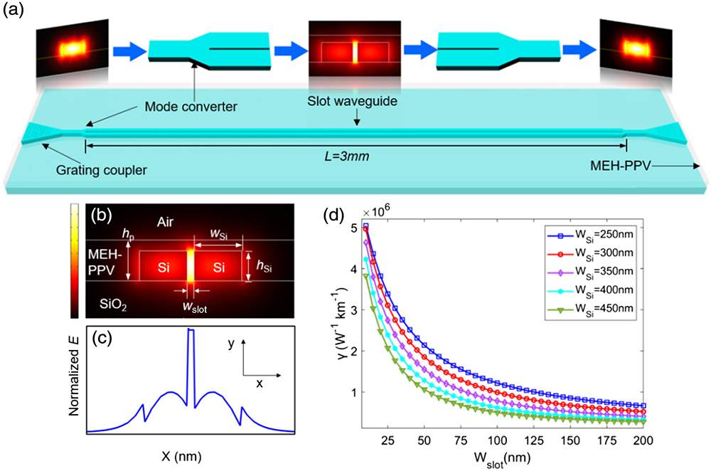
Figure 1.(a) Schematic diagram of the highly nonlinear SOHSW. (b) Normalized electric field distribution and (c) corresponding normalized magnitude of the SOHSW. (d) Evolution of the nonlinear coefficient
The nonlinear coefficient of the SOHSW is estimated for each material in the slot waveguide and scaled via the respective fractional energy
Parameters Used to Calculate the Effective Nonlinear Coefficient of the SOHSW
| Material | |||
|---|---|---|---|
| MEH-PPV | 1.65 | 0.019133 | |
| Si | 3.48 | 0.120470 | |
| 1.48 | 0.051590 |
B. Nonlinearity Measurement of MEH-PPV
The MEH-PPV cladding layer is created by first dissolving 20 mg of MEH-PPV powder (Shanghai Aladdin Biochemical Technology Co., Ltd., average molecular weight 70,000–100,000) into 1.5 mL of toluene. The solution is then magnetically stirred at a temperature of 70°C for 24 h. To create the MEH-PPV cladding sample, the MEH-PPV solution is spin coated onto a silica wafer to produce a 0.8 μm film. The nonlinear characteristics of the MEH-PPV film are measured using the Z-scan method [33]. The experimental setup is depicted in Fig. 2(a). An input Gaussian laser beam is obtained using a femtosecond laser (Carbide CB5, pulse width 216 fs, repetition frequency 1 kHz) at a wavelength of 1030 nm, and the wavelength is converted to 1550 nm by an optical parametric amplifier. The converted beam is focused through a convex lens (focal length 200 mm) and transmitted through the sample into a beam splitter. The transmission branch is received through a finite aperture in the far field and detected by detector D1 to measure the nonlinear index, while the reflected branch is received by detector D2, which does not contain an aperture to measure the nonlinear absorption. On both detectors, the transmittance of MEH-PPV is measured as a function of the sample position
![]()
Figure 2.(a) Experimental setup for the Z-scan measurement. (b) Closed aperture scan of a 0.8 μm thick MEH-PPV film with 1 mm thick fused silica substrate. (c) Open aperture scan of the MEH-PPV film for absorption measurement. (d) Closed aperture scan of a 1 mm thick fused silica substrate.
One condition that must be met when making the open aperture scan in the far field region is that the distance from the sample to the aperture must be far greater than the Rayleigh length of the beam. In this case, the nonlinear index
The experimental settings of the Z-scan of the MEH-PPV film are shown in detail in Table 2. Figure 2(b) illustrates the data collected during the closed aperture scan of a 0.8 μm thick MEH-PPV film on a 1 mm thick fused silica substrate at the peak intensity of
Experimental Parameters for the Closed Aperture Scan
| Input Power (μW) | ||||
|---|---|---|---|---|
| 95.6 | 0.8 | 0.13 | 1.66 | 29.1 |
To estimate the influence of the silica substrate on the nonlinear index of the polymer, we also measure a closed aperture scan of a bare 1 mm thick silica substrate with the same peak intensity as shown in Fig. 2(d). The results of this measurement show that the nonlinear refraction in the fused silica is extremely weak and support that it is reasonable to attribute the nonlinear refraction to the MEH-PPV film only. Based on the above measurements and Eqs. (3)–(5), the nonlinear index of MEH-PPV is calculated to be
C. Fabrication of the SOHSW
The device is fabricated on a standard SOI wafer with a silicon thickness of 220 nm and a buried-oxide thickness of 2 μm. Figure 3(a) illustrates the fabrication steps used to create the SOHSW. The device pattern is transferred to the silicon layer using EBL and ICP etching. For the lithography steps [step i in Fig. 3(a)], we use a high-resolution nanolithography system (Raith EBPG5150) to obtain an ultranarrow slot. In addition, to obtain both high precision and a high-etching selection ratio, a positive high-contrast e-beam resist ARP-6200 (CSA-62) is adopted as the mask. The difficulty to create an ultranarrow slot area relies on the etching gas diffusion in the nano slot with a high aspect ratio, as well as the etching rate ununiformity induced by the loading effect depending on the different feature sizes. Specifically, for the silicon waveguide based on the 220 nm SOI wafer, the etching region on each side of the nanostructure is usually as wide as a few micrometers (i.e., ① ② in step ii), which is much wider than the slot width. Thus, during etching, the etching gas diffuses more slowly in the narrow slot than on both sides, resulting in a slower etching rate of the slot correspondingly. In this case, when the side regions reach the depth of 220 nm, the slot depth is still less than 220 nm. This issue is well resolved in our fabrication by over etching the substrate (ii and iii) and fine-tuning the etching recipe. In this way, the side regions are over etched into the silica layer where the side regions are slightly deeper than 220 nm, while the slot can just be fully etched. Note that the over etching, however, will not affect the light transmission much since the refractive index of MEH-PPV is close to that of silica. In addition, the etching rate of silica is much lower than that of silicon so that the over etched substrate will not be too deep in our fabrication. Another important point is that the thickness of the photoresist should be well optimized. If the photoresist is too thin, the silicon waveguide might also be etched during the over etching process, while if too thick, the resolution of the e-beam lithography would be reduced due to the electron scattering and proximity effect. Thus, the resist thickness, lithography parameters, and etching parameters need to be comprehensively optimized to obtain the ultranarrow slot. In our fabrication, the 45 nm narrow slot is successfully achieved with the following fabrication parameters: (1) 400 nm thick photoresist ARP-6200; (2) EBL acceleration voltage of 100 kV, beam current of 0.5 nA, and exposure dose of
![]()
Figure 3.(a) Illustration of the device fabrication steps of the presented SOHSW. (b) Scanning electron microscopy images of the fabricated device.
3. SYSTEM EXPERIMENTS
A. Enhanced Nonlinear Coefficient of the SOHSW
The nonlinear performance of the SOHSW is characterized by assessing the conversion of DFWM with two continuous waves (CWs) [23], of which the stronger wave is referred to as the pump, while the weaker one is the signal. Figure 4(a) shows the corresponding experimental setup. Two CW beams (Alnair Labs, TLG-200) with respective wavelengths of 1542.5 nm (P1) and 1544.1 nm (S1) are amplified and then multiplexed with the input grating coupler in the SOHSW. A polarization controller (PC) is used in each channel after the amplification to optimize the incident CW polarization in the transverse electric (TE) mode. The average powers of P1 and S1 measured at the output of the dense wavelength division multiplexer (DWDM) are 24 dBm and 19 dBm, respectively. Taking the coupling loss of 5 dB/facet into account, the respective average powers of the two pumps involved in the SOHSW are 19 dBm and 14 dBm. The FWM performance is observed at the output grating coupler via an optical spectrum analyzer (OSA, Yokogawa, AQ6370D).
![]()
Figure 4.(a) Experimental setup used to measure the nonlinear coefficients. (b) FWM spectra of the SOHSW (red curve) and bare silicon slot waveguide (blue curve). (c) FWM spectra of the SOHSW (red curve) and strip waveguide (
Based on the DFWM, the nonlinear coefficient
Figure 4(b) displays the FWM spectra measured for the SOHSW (red line) and the bare silicon slot waveguide without the MEH-PPV film (blue line). Both nanostructures have lengths of 3 mm. As illustrated in Fig. 4(b), the conversion efficiency using the SOHSW is measured as
Parameters Used to Calculate
| Waveguide | ||||||
|---|---|---|---|---|---|---|
| SOHSW | 3 | 4.56 | 19 | 767 | 0.0018 | |
| Slot waveguide | 3 | 10.53 | 18.5 | 732 | 0.0001 | |
| Strip waveguide | 3 | −0.80 | 17 | 87 | 0.0005 |
B. SOHSW for All-Optical High-Speed Logic Operations
The enhanced nonlinearity in the SOHSW makes the nanostructured device a good candidate for all-optical high-speed signal processing. Here, as a proof of concept, we experimentally demonstrate 40 Gb/s all-optical canonical logic units, performing as the basic building blocks for complexed reconfigurable logic functions. The experimental setup is shown in Fig. 5. Two return-to-zero differential phase-shift keying (RZ-DPSK) signals with a bit rate of 40 Gb/s and a duty cycle of 33% are generated using a transmitter (Tx) with a
![]()
Figure 5.Experimental setup for the 40 Gb/s all-optical logic canonical units based on the SOHSW.
Figure 6 shows the measured spectrum of FWM created by signals A and B. One can see that the logic information, i.e., A AND B (AB), is multicasted to both idlers. According to the spectrum, the conversion efficiency of the target idler is estimated as about
![]()
Figure 6.Measured FWM spectrum achieved at the output of SOHSW.
Figures 7(a) and 7(b) illustrate the temporal waveforms of the original signals and logic results observed by the communication signal analyzer (CSA), respectively. It is found from Fig. 7 that the logic levels are clearly identified, and the logic sequences are correct with wide open eyes, resulting in extinction ratios higher than 12 dB. Additionally, as shown in Fig. 8, all logic results exhibit error-free performance with a power penalty less than
![]()
Figure 7.Temporal waveforms and eye diagrams of the original signals and logical results.
![]()
Figure 8.Bit error rate (BER) measurements for the original signals and logic operations.
4. CONCLUSION
In summary, we propose and experimentally demonstrate a highly nonlinear silicon–organic slot waveguide for ultrafast all-optical signal processing and communication. Here, the nonlinearity of the chip is greatly enhanced by optical field confinement in a 45 nm wide slot that is filled with a nonlinear polymer MEH-PPV. To the best of our knowledge, this is the narrowest slot width that has ever been experimentally realized in silicon slot waveguides. Also, the organic polymer is easily obtained without the need for additional synthesis steps and also shows good nonlinear characteristics demonstrated by Z-scan. The nonlinear coefficient of SOHSW is then investigated through DFWM. The results show that the SOHSW offers obvious conversion efficiency enhancements of more than 12 dB and 5 dB compared to those achieved in a bare silicon slot waveguide and a strip waveguide, respectively. From the results, the nonlinear coefficient of the fabricated SOHSW is calculated to be as high as
Acknowledgment
Acknowledgment. The authors extend their sincere thanks to Professor Shunbin Lu at Shenzhen University for the assistance of Z-scan measurements.
References
[1] I. L. Markov. Limits on fundamental limits to computation. Nature, 512, 147-154(2014).
[2] A. E. Willner, S. Khaleghi, M. R. Chitgarha, O. F. Yilmaz. All-optical signal processing. J. Lightwave Technol., 32, 660-680(2014).
[3] L. Lei, J. Dong, B. Zou, Z. Wu, W. Dong, X. Zhang. Expanded all-optical programmable logic array based on multi-input/output canonical logic units. Opt. Express, 22, 9959-9970(2014).
[4] G. Lu, T. Sakamoto, T. Kawanishi. Wavelength conversion of optical 64QAM through FWM in HNLF and its performance optimization by constellation monitoring. Opt. Express, 22, 15-22(2014).
[5] J. Qiu, K. Sun, M. Rochette, L. R. Chen. Reconfigurable all-optical multilogic gate (XOR, AND, and OR) based on cross-phase modulation in a highly nonlinear fiber. IEEE Photon. Technol. Lett., 22, 1199-1201(2010).
[6] J. Qin, G. Lu, T. Sakamoto, K. Akahane, N. Yamamoto, D. Wang, C. Wang, H. Wang, M. Zhang, T. Kawanishi, Y. Ji. Simultaneous multichannel wavelength multicasting and XOR logic gate multicasting for three DPSK signals based on four-wave mixing in quantum-dot semiconductor optical amplifier. Opt. Express, 22, 29413-29423(2014).
[7] N. Deng, K. Chan, C. K. Chan, L. K. Chen. An all-optical XOR logic gate for high-speed RZ-DPSK signals by FWM in semiconductor optical amplifier. IEEE J. Sel. Top. Quantum Electron., 12, 702-707(2006).
[8] J. Wang, J. Sun, Q. Sun. Single-PPLN-based simultaneous half-adder, half-subtracter, and OR logic gate: proposal and simulation. Opt. Express, 15, 1690-1699(2007).
[9] Q. Lin, O. J. Painter, G. P. Agrawal. Nonlinear optical phenomena in silicon waveguides: modeling and applications. Opt. Express, 15, 16604-16644(2007).
[10] M. Dinu, F. Quochi, H. Garcia. Third-order nonlinearities in silicon at telecom wavelengths. Appl. Phys. Lett., 82, 2954-2956(2003).
[11] C. Koos, L. Jacome, C. Poulton, J. Leuthold, W. Freude. Nonlinear silicon-on-insulator waveguides for all-optical signal processing. Opt. Express, 15, 5976-5990(2007).
[12] E. Timurdogan, C. V. Poulton, M. J. Byrd, M. R. Watts. Electric field-induced second-order nonlinear optical effects in silicon waveguides. Nat. Photonics, 11, 200-206(2017).
[13] D. J. Moss, R. Morandotti, A. L. Gaeta, M. Lipson. New CMOS-compatible platforms based on silicon nitride and Hydex for nonlinear optics. Nat. Photonics, 7, 597-607(2013).
[14] R. Salem, M. A. Foster, A. C. Turner, D. F. Geraghty, M. Lipson, A. L. Gaeta. Signal regeneration using low-power four-wave mixing on silicon chip. Nat. Photonics, 2, 35-38(2008).
[15] J. Leuthold, C. Koos, W. Freude. Nonlinear silicon photonics. Nat. Photonics, 4, 535-544(2010).
[16] P. Steglich, C. Mai, C. Villringer, B. Dietzel, S. Bondarenko, V. Ksianzou, F. Villasmunta, C. Zesch, S. Pulwer, M. Burger. Silicon-organic hybrid photonics: an overview of recent advances, electro-optical effects and CMOS integration concepts. J. Phys. Photon., 3, 022009(2021).
[17] P. Steglich, C. Mai, A. Mai. Silicon-organic hybrid photonic devices in a photonic integrated circuit technology. ECS J. Solid State Sci. Technol., 8, Q217-Q221(2019).
[18] W. Heni, Y. Kutuvantavida, C. Haffner, H. Zwickel, C. Kieninger, S. Wolf, M. Lauermann, Y. Fedoryshyn, A. F. Tillack, L. E. Johnson, D. L. Elder, B. H. Robinson, W. Freude, C. Koos, J. Leuthold, L. R. Dalton. Silicon–organic and plasmonic–organic hybrid photonics. ACS Photon., 4, 1576-1590(2017).
[19] J. Leuthold, W. Freude, J. M. Brosi, R. Baets, P. Dumon, I. Biaggio, M. L. Scimeca, F. Diederich, B. Frank, C. Koos. Silicon organic hybrid technology—a platform for practical nonlinear optics. Proc. IEEE, 97, 1304-1316(2009).
[20] J. Leuthold, C. Koos, W. Freude, L. Alloatti, R. Palmer, D. Korn, J. Pfeifle, M. Lauermann, R. Dinu, S. Wehrli, M. Jazbinsek, P. Gunter, M. Waldow, T. Wahlbrink, J. Bolten, H. Kurz, M. Fournier, J. M. Fedeli, Y. Hui, W. Bogaerts. Silicon-organic hybrid electro-optical devices. IEEE J. Sel. Top. Quantum Electron., 19, 114-126(2013).
[21] Z. Xingyu, A. Hosseini, L. Xiaohui, H. Subbaraman, R. T. Chen. Polymer-based hybridintegrated photonic devices for silicon on-chip modulation and board-level optical interconnects. IEEE J. Sel. Top. Quantum Electron., 19, 3401115(2013).
[22] T. W. Baehr-Jones, M. J. Hochberg. Polymer silicon hybrid systems: a platform for practical nonlinear optics. J. Phys. Chem. C, 112, 8085-8090(2008).
[23] C. Koos, P. Vorreau, T. Vallaitis, P. Dumon, W. Bogaerts, R. Baets, B. Esembeson, I. Biaggio, T. Michinobu, F. Diederich, W. Freude, J. Leuthold. All-optical high-speed signal processing with silicon–organic hybrid slot waveguides. Nat. Photonics, 3, 216-219(2009).
[24] B. Arijit, K. Markku, H. Seppo, R. Matthieu. Silicon slot waveguide Fano resonator. Opt. Lett., 43, 3489-3492(2018).
[25] S. Ummethala, J. N. Kemal, A. S. Alam, M. Lauermann, A. Kuzmin, Y. Kutuvantavida, S. H. Nandam, L. Hahn, D. L. Elder, L. R. Dalton, T. Zwick, S. Randel, W. Freude, C. Koos. Hybrid electro-optic modulator combining silicon photonic slot waveguides with high-k radio-frequency slotlines. Optica, 8, 511-519(2021).
[26] B. L. Lawrence, M. Cha, J. U. Kang, W. Toruellas, G. Stegeman, G. Baker, J. Meth, S. Etemad. Large purely refractive nonlinear index of single crystal P-toluene sulphonate (PTS) at 1600 nm. Electron. Lett., 30, 447-448(1994).
[27] S. Polyakov, F. Yoshino, M. Liu, G. Stegeman. Nonlinear refraction and multiphoton absorption in polydiacetylenes from 1200 to 2200 nm. Phys. Rev. B, 69, 115421(2004).
[28] M. T. Beels, M. S. Fleischman, I. Biaggio, B. Breiten, M. Jordan, F. Diederich. Compact TCBD based molecules and supramolecular assemblies for third-order nonlinear optics. Opt. Mater. Express, 2, 294-303(2012).
[29] J. Covey, A. D. Finke, X. Xu, W. Wu, Y. Wang, F. Diederich, R. T. Chen. All-optical switching with 1-ps response time in a DDMEBT enabled silicon grating coupler/resonator hybrid device. Opt. Express, 22, 24530-24544(2014).
[30] P. A. Anderson, B. S. Schmidt, M. Lipson. High confinement in silicon slot waveguides with sharp bends. Opt. Express, 14, 9197-9202(2006).
[31] M. P. Nielsen, X. Shi, P. Dichtl, S. A. Maier, R. F. Oulton. Giant nonlinear response at a plasmonic nanofocus drives efficient four-wave mixing. Science, 358, 1179-1181(2017).
[32] R. F. Oulton, G. Bartal, D. F. P. Pile, X. Zhang. Confinement and propagation characteristics of subwavelength plasmonic modes. New J. Phys., 10, 105018(2008).
[33] M. Samoc, A. Samoc, B. Luther-Davies. Third harmonic autocorrelation and wave mixing in a thin film of poly(p-phenylenevinylene). Opt. Express, 11, 1787-1792(2003).
[34] M. P. Nielsen, L. Lafone, A. Rakovich, T. Sidiropoulos, M. Rahmani, S. A. Maier, R. F. Oulton. Oulton Adiabatic nanofocusing in hybrid gap plasmon waveguide on the silicon-on-insulator platform. Nano Lett., 16, 1410-1414(2016).
[35] M. Ono, M. Hata, M. Tsunekawa, K. Nozaki, H. Sumikura, H. Chiba, M. Notomi. Ultrafast and energy-efficient all-optical switching with graphene-loaded deep-subwavelength plasmonic waveguides. Nat. Photonics, 14, 37-43(2020).
[36] M. Sheik-Bahae, A. A. Said, T. Wei, D. J. Hagan, E. W. Van Stryland. Sensitive measurement of optical nonlinearities using a single beam. IEEE J. Quantum Electron., 26, 760-769(1990).
[37] M. A. Foster, A. C. Turner, J. E. Sharping, B. S. Schmidt, M. Lipson, A. L. Gaeta. Broad-band optical parametric gain on a silicon photonic chip. Nature, 441, 960-963(2006).
[38] A. B. Fallahkhair, K. S. Li, T. E. Murphy. Vector finite difference modesolver for anisotropic dielectric waveguides. J. Lightwave Technol., 26, 1423-1431(2008).


Set citation alerts for the article
Please enter your email address

© Copyright 2018-2021 | Chinese Laser Press. All Rights Reserved 沪ICP备15018463号-20