
Yiyin Zhou, Solomon Ojo, Chen-Wei Wu, Yuanhao Miao, Huong Tran, Joshua M. Grant, Grey Abernathy, Sylvester Amoah, Jake Bass, Gregory Salamo, Wei Du, Guo-En Chang, Jifeng Liu, Joe Margetis, John Tolle, Yong-Hang Zhang, Greg Sun, Richard A. Soref, Baohua Li, Shui-Qing Yu, "Electrically injected GeSn lasers with peak wavelength up to 2.7 μm," Photonics Res. 10, 222 (2022)
- Photonics Research
- Vol. 10, Issue 1, 222 (2022)
Abstract
1. INTRODUCTION
SiGeSn alloys have attracted considerable attention in recent years as a versatile material system enabling all-group-IV-based optoelectronic device integration [1,2]. Specifically, direct-bandgap GeSn offers a route toward monolithic integration of light sources on Si for mid-infrared applications [3]. The first set of GeSn lasers was demonstrated under optical pumping at temperatures up to 90 K [4]. Since then, the studies of GeSn lasers have made inspiring leaps in maximum operating temperature (
The electrically injected GeSn laser diode is of even greater interest, as it can be fully integrated on the Si-based group-IV photonics platform. However, to achieve lasing under electrical injection involves more challenges than that under optical pumping. For example, extra sources of optical loss are introduced by the metal contacts and doping. The metal is highly absorptive so that extra layers are needed to isolate the metal away from the optical mode while maintaining a decent electrical conduction. Such layers require more precise control during the material growth. Another challenge is the increased free carrier absorption (FCA) loss due to increased doping for more effective carrier injection through a pn junction, which increases laser threshold in comparison with optically pumped lasers, where carrier injection is easily achieved with the optical absorption of the pump light.
Such differences illustrate the need to design and evaluate the laser structures under electrical injection. Recently, an electrically pumped laser operational up to 100 K was demonstrated [14]. The devices had a minimum threshold at
Sign up for Photonics Research TOC. Get the latest issue of Photonics Research delivered right to you!Sign up now
In this work, several electrically injected GeSn heterostructure laser diodes with different cap layers and active layer materials were compared. Increased cap thickness improves the optical confinement factor in the gain region and reduces the optical loss from the metal contact significantly. The devices with a thicker cap layer demonstrated reduced threshold, compared to the devices with a thinner cap. Cap layer materials with different conduction band barrier heights were also studied. The
2. EXPERIMENT
A. Layer Structure of the Laser Diodes
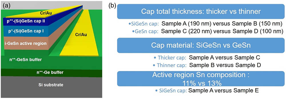
Figure 1.(a) 3D schematic of the ridge waveguide laser designed structure; (b) three experiment groups are studied with tuning of the total cap thickness, cap layer material, and active region Sn composition.
B. Device Fabrication
The laser diode devices were fabricated into ridge waveguide laser structure. The 80 μm wide ridge structure was formed by standard photolithography and wet chemical etching. The ridge was etched to the n-type GeSn buffer (200 nm etched into the buffer layer). The metal contacts (
C. Experimental Design
Three sets of experiments were designed to study the GeSn laser structures, summarized in Fig. 1(b). The first set adjusts the total thickness of the cap layer in order to evaluate the optical mode-profile effect on the optical confinement factor as well as the absorption loss. Samples A and C have the designed total cap thickness of 190 nm compared to 150 nm in samples B and D, respectively. The second variable is the material used in the cap layers that changes conduction-band barrier height in the heterostructure.
D. Experimental Methods
The photoluminescence (PL) was measured from the cap-removed sample. The heterostructure sample was chemically etched, the top 600 nm of the structure was removed, and the active region was exposed at the surface for PL characterization. The sample surface was excited by using the 532 nm continuous-wave laser at 500 mW. The emission was collected through the spectrometer with the InSb detector. The signal was recorded via a standard lock-in technique.
For the electrically injected laser measurement, the chip was mounted in a temperature-controlled cryostat for the characterization. The device operated under a pulsed mode to avoid Joule heating. The pulsed voltage source was used as the pumping source with a 1 kHz repetition rate and 700 ns of pulse width. The emission power and spectra were characterized using a grating-based spectrometer equipped with a liquid-nitrogen-cooled InSb detector (detection range 1.0–5.5 μm). The spectra presented in this paper focus on comparing the peak wavelength and on demonstrating the emission below and above the lasing threshold. Therefore, the resolution of the spectrometer is set at 10 nm, which is compromised to obtain a reasonable signal-to-noise ratio for the spectrum, especially at the low intensity level below the threshold. The absolute optical power was measured using a calibrated power meter. The emission from the facet was coupled by a pair of convex lenses and focused on the power meter. Note that the reflection and absorption losses through the cryostat window and lens were calculated and were added to the power meter readout aiming to report more accurate emission power. The emission was then guided onto the InSb detector through the spectrometer for the light output-current injection (L-I) and spectral measurements. The detailed description of the high-resolution spectra and the absolute power calibration process can be found in Ref. [14].
3. RESULTS
A. Observation of Lasing
To validate the lasing operation, the devices characteristics were measured using the same method that was detailed in Ref. [14]. According to measurement results, all devices show unambiguous lasing characteristics, as the threshold indicating the onset of lasing, dramatically reduced peak linewidth, and increased peak intensity were clearly observed, which were acknowledged to identify the lasing of sample A in Ref. [14]. The typical characterization results of sample E are shown in Fig. 2.
![]()
Figure 2.Characterizations of sample E. (a) Temperature-dependent L-I curve. (b) Lasing spectra under injections below and above threshold at 10 K. The PL spectrum was also plotted for comparison. (c) Emission spectra under injections below and above threshold at 90 K; inset: semi-log plot of the spectra.
Figure 2(a) displays the temperature-dependent L-I curves for sample E. The threshold characteristic can be clearly resolved. The lasing was observed at temperatures from 10 K to 90 K, with the threshold from 1.4 to
Figure 2(b) shows the emission spectra below and above the lasing threshold at 10 K. The PL spectrum at 10 K was also plotted for comparison (dotted line). Compared to the PL peak, the significantly reduced emission peak linewidth indicates the onset of lasing. Note that based on our previous study [5,7,14], the devices feature multimode operation, and therefore the observed peak actually consists of multimode peaks [e.g., see the spectra in Fig. 2(b) for
B. Light Output-Current Injection Characteristics
The L-I curves of all devices at 10 K are plotted in Fig. 3(a). Sample A features the lowest threshold while sample D has the highest threshold, which are 0.6 and
![]()
Figure 3.L-I curves of each sample at (a) 10 K, (b) 50 K, and (c) 90 K.
As temperature increases, sample D stops lasing above 10 K. Figure 3(b) shows L-I curves of all other samples at 50 K. The lowest and highest thresholds are
As temperature further increases, sample B stops lasing above 50 K. The L-I curves of samples A, C, and E at 90 K are shown in Fig. 3(c), with the corresponding thresholds of 1.8, 5.1, and
Figure 4 shows the laser peak emission under injection of
![]()
Figure 4.Normalized spectra showing the lasing peaks under
For samples A to E, the full widths at half-maximum (FWHMs) incorporating all lasing modes were measured as 32, 29, 18, 34, and 16 nm (under the 10 nm resolution spectrometer), respectively, at 10 K. Note that these FWHMs represent the gain spectral width rather than the true lasing peak width since each incorporates a series of longitudinal modes that cannot be resolved at 10 nm resolution. Our previous studies revealed that due to the relatively large area of the cross section, all laser devices feature multimode operation. The high-resolution lasing spectra showing well-resolved multi-peaks of sample A were reported in Ref. [14]. The characteristics for all laser devices are summarized in Table 2.
Summary of Laser Characteristics
| Sample | Cap Layer Material | Cap Layer | Sn Composition in | Threshold | Threshold | Lasing | ||
|---|---|---|---|---|---|---|---|---|
| A | 190 | 11 | 0.6 | 1.4 | 100 | 76 | 2238 | |
| B | 150 | 11 | 1.4 | N.A. | 50 | 119 | 2281 | |
| C | 220 | 11 | 2.4 | 3.1 | 90 | 123 | 2294 | |
| D | 100 | 11 | 3.4 | N.A. | 10 | N.A. | 2272 | |
| E | 180 | 13 | 1.4 | 2.9 | 90 | 81 | 2654 |
4. DISCUSSION
A. Thickness of Cap Layer [First Experimental Group in Fig.
The total thickness of the cap layer considerably affects the lasing performance. Both comparisons (A versus B and C versus D) show the same trend, no matter whether SiGeSn or GeSn is used as cap layer material—that a thicker cap device has a lower lasing threshold as well as higher maximum operating temperature: at 10 K, sample A has a threshold that is 0.43 of that of sample B, while sample C has a lower threshold that is 0.70 of sample D. For the maximum operating temperature, 100 K for sample A versus 50 K for sample B, and 90 K for sample C versus 10 K for sample D, were observed. The change of cap layer thickness affects the laser performance by the following factors: (i) optical loss from the metal contact playing the major role, (ii) FCA within the heavily doped cap layers, and (iii) the optical confinement factor in the active region.
![]()
Figure 5.Calculated metal absorption loss and FCA loss in p-type cap layer for sample A as functions of SiGeSn cap layer total thickness.
The FCA loss for each layer was calculated based on the doping level and the carrier injection [17] as summarized in Table 3. A considerable amount of FCA is introduced in the active region, serving as the second dominating loss mechanism. The n-type-doped GeSn buffer shows a relatively small value (
Overall, it can be seen that the higher total loss results in a larger threshold, comparing B to A (or D to C). The metal absorption loss dramatically decreases as the cap layer thickness increases, while the FCA loss shows limited change. As a result, the total loss would not further decrease with the thicker cap. Moreover, with very thick cap layer (
B. Cap Layer Materials [Second Experimental Group in Fig.
The cap layer also serves as the top energy barrier with respect to active region. The
The conduction band (CB) barrier height of each sample was calculated. For both comparisons (A versus C and B versus D:
The VB barrier height between the GeSn active and the GeSn buffer was calculated for each sample as well. Samples A to D show similar hole barrier height of
Note that the accurate band offset has not been experimentally verified so far, and the actual band alignment remains uncertain. However, the difference between barrier height has its significance to show the general laser structure behavior qualitatively.
C. Sn Compositions in the Active Region [Third Experimental Group in Fig.
Samples A (
D. Additional Consideration
In addition to the abovementioned loss mechanism, other factors that affect the device performance are elaborated as follows. (i) Active layer thickness. In this work, the design of sample structure is inherited from the former optically pumped lasers, in which a thicker active layer is preferred, aiming to have higher light absorption. However, such absorption enhancement with a thicker active layer does not apply to electrically injected lasers. In fact, growing a thinner active region could effectively reduce the threshold [21]. (ii) Absorption loss in the GeSn buffer and the SiGeSn/GeSn cap. Since the GeSn buffer is almost relaxed and heavily doped, the high density of dislocations due to lattice mismatch would create defect energy levels in the bandgap, resulting in additional absorption loss. The absorption tails have been reported in GeSn materials, which leads to below-bandgap absorption with the orders of
5. CONCLUSIONS
In conclusion, electrically injected GeSn laser diodes were studied with an evaluation of three factors in the structure: cap layer thickness, cap materials, and active region materials. The thicker capped devices feature lower metal absorption loss, offering a reduction of threshold and an elevation of maximum operating temperature. The devices with a
Acknowledgment
Acknowledgment. Dr. Wei Du appreciates support from Provost’s Research & Scholarship Fund at Wilkes University.
References
[1] R. Soref. Mid-infrared photonics in silicon and germanium. Nat. Photonics, 4, 495-497(2010).
[2] R. Soref, D. Buca, S.-Q. Yu. Group IV photonics: driving integrated optoelectronics. Opt. Photon. News, 27, 32-39(2016).
[3] X. Wang, J. Liu. Emerging technologies in Si active photonics. J. Semicond., 39, 061001(2018).
[4] S. Wirths, R. Geiger, N. von den Driesch, G. Mussler, T. Stoca, S. Mantl, Z. Ikonic, M. Luysberg, S. Chiussi, J. M. Hartmann, H. Sigg, J. Faist, D. Buca, D. Grützmacher. Lasing in direct-bandgap GeSn alloy grown on Si. Nat. Photonics, 9, 88-92(2015).
[5] J. Margetis, S. Al-Kabi, W. Du, W. Dou, Y. Zhou, T. Pham, P. Grant, S. Ghetmiri, A. Mosleh, B. Li, J. Liu, G. Sun, R. Soref, J. Tolle, M. Mortazavi, S.-Q. Yu. Si-based GeSn lasers with wavelength coverage of 2–3 μm and operating temperatures up to 180 K. ACS Photon., 5, 827-833(2017).
[6] Q. Thai, N. Pauc, J. Aubin, M. Bertrand, J. Chrétien, V. Delaye, A. Chelnokov, J. Hartmann, V. Reboud, V. Calvo. GeSn heterostructure micro-disk laser operating at 230 K. Opt. Express, 26, 32500-32508(2018).
[7] Y. Zhou, W. Dou, W. Du, S. Ojo, H. Tran, S. Ghetmiri, J. Liu, G. Sun, R. Soref, J. Margetis, J. Tolle, B. Li, Z. Chen, M. Mortazavi, S.-Q. Yu. Optically pumped GeSn lasers operating at 270 K with broad waveguide structures on Si. ACS Photon., 6, 1434-1441(2019).
[8] J. Chrétien, N. Pauc, F. Armand Pilon, M. Bertrand, Q. Thai, L. Casiez, N. Bernier, H. Dansas, P. Gergaud, E. Delamadeleine, R. Khazaka, H. Sigg, J. Faist, A. Chelnokov, V. Reboud, J. Hartmann, V. Calvo. GeSn lasers covering a wide wavelength range thanks to uniaxial tensile strain. ACS Photon., 6, 2462-2469(2019).
[9] A. Elbaz, D. Buca, N. von den Driesch, K. Pantzas, G. Patriarche, N. Zerounian, E. Herth, X. Checoury, S. Sauvage, I. Sagnes, A. Foti, R. Ossikovski, J. Hartmann, F. Boeuf, Z. Ikonic, P. Boucaud, D. Grützmacher, M. El Kurdi. Ultra-low threshold cw and pulsed lasing in tensile strained GeSn alloys. Nat. Photonics, 14, 375-382(2020).
[10] W. Du, Q. M. Thai, J. Chrétien, M. Bertrand, L. Casiez, Y. Zhou, J. Margetis, N. Pauc, A. Chelnokov, V. Reboud, V. Calvo, J. Tolle, B. Li, S.-Q. Yu. Study of Si-based GeSn optically pumped lasers with micro-disk and ridge waveguide structures. Front. Phys., 7, 147(2019).
[11] D. Stange, S. Wirths, R. Geiger, C. Schulte-Braucks, B. Marzban, N. von den Driesch, G. Mussler, T. Zabel, T. Stoica, J.-M. Hartmann, S. Mantl, Z. Ikonic, D. Grützmacher, H. Sigg, J. Witzens, D. Buca. Optically pumped GeSn microdisk lasers on Si. ACS Photon., 3, 1279-1285(2016).
[12] D. Stange, N. von den Driesch, T. Zabel, F. Armand-Pilon, D. Rainko, B. Marzban, P. Zaumseil, J. Hartmann, Z. Ikonic, G. Capellini, S. Mantl, H. Sigg, J. Witzens, D. Grützmacher, D. Buca. GeSn/SiGeSn heterostructure and multi quantum well lasers. ACS Photon., 5, 4628-4636(2018).
[13] J. Margetis, Y. Zhou, W. Dou. All group-IV SiGeSn/GeSn/SiGeSn QW laser on Si operating up to 90 K. Appl. Phys. Lett., 113, 221104(2018).
[14] Y. Zhou, Y. Miao, S. Ojo, H. Tran, G. Abernathy, J. M. Grant, S. Amoah, G. Salamo, W. Du, J. Liu, J. Margetis, J. Tolle, Y.-H. Zhang, G. Sun, R. A. Soref, B. Li, S.-Q. Yu. Electrically injected GeSn lasers on Si operating up to 100 K. Optica, 7, 924-929(2020).
[15] S. A. Ghetmiri, W. Du, B. R. Conley, A. Mosleh, A. Nazzal, G. Sun, R. A. Soref, J. Margetis, T. Joe, H. A. Naseem, S. Q. Yu. Shortwave-infrared photoluminescence from Ge1-
[16] E. Garmire, H. Stoll. Propagation losses in metal-film-substrate optical waveguides. IEEE J. Quantum Electron., 8, 763-766(1972).
[17] G. E. Chang, S. W. Chang, S. L. Chuang. Theory for n-type doped, tensile-strained Ge-Si
[18] C. Chaminant, J. Charil, J.-C. Bouley, E. V. K. Rao. Growth and properties of GaAsSb/GaAIAsSb double heterostructure lasers. IEEE Trans. Electron. Dev., 3, 196-200(1979).
[19] Y. Zhou, W. Dou, W. Du, T. Pham, S. A. Ghetmiri, S. Al-Kabi, A. Mosleh, M. Alher, J. Margetis, J. Tolle, G. Sun, R. Soref, B. Li, M. Mortazavi, H. Naseem, S.-Q. Yu. Systematic study of GeSn heterostructure-based light-emitting diodes towards mid-infrared applications. J. Appl. Phys., 120, 023102(2016).
[20] M. Bertrand, N. Pauc, Q. M. Thai, J. Chrétien, L. Casiez, A. Quintero, P. Rodriguez, R. Khazaka, J. Aubin, J. M. Hartmann, A. Chelnokov, V. Calvo, V. Reboud. Mid-infrared GeSn-based LEDs with Sn content up to 16%. IEEE 16th International Conference on Group IV Photonics, 1-2(2019).
[21] S. L. Chuang. Physics of Photonic Devices, 416-417.
[22] S. V. Kondratenko, Yu. V. Hyrka, Yu. I. Mazur, A. V. Kuchuk, W. Dou, H. Tran, J. Margetis, J. Tolle, S.-Q. Yu, G. J. Salamo. Photovoltage spectroscopy of direct and indirect bandgaps of strained Ge1-
[23] H. Tran, W. Du, S. Ghetmiri, A. Mosleh, G. Sun, R. Soref, J. Margetis, J. Tolle, B. Li, H. Naseem, S.-Q. Yu. Systematic study of Ge1−


Set citation alerts for the article
Please enter your email address

© Copyright 2018-2021 | Chinese Laser Press. All Rights Reserved 沪ICP备15018463号-20