• Photonics Research
  • Vol. 10, Issue 1, 197 (2022)
Mingxing Li1、2, Yueke Wang1、2、4、*, Tian Sang1、2、5、*, Hongchen Chu3、6、*, Yun Lai3, and Guofeng Yang1、2
Author Affiliations
  • 1Optical Information Science and Technology Department, Jiangnan University, Wuxi 214122, China
  • 2Optoelectronic Engineering and Technology Research Center, Jiangnan University, Wuxi 214122, China
  • 3National Laboratory of Solid State Microstructures, School of Physics, and Collaborative Innovation Center of Advanced Microstructures, Nanjing University, Nanjing 210093, China
  • 4e-mail: ykwang@jiangnan.edu.cn
  • 5e-mail: sangt@jiangnan.edu.cn
  • 6e-mail: chuhongchen@nju.edu.cn
  • show less
    DOI: 10.1364/PRJ.440640 Cite this Article Set citation alerts
    Mingxing Li, Yueke Wang, Tian Sang, Hongchen Chu, Yun Lai, Guofeng Yang. Experimental observation of multiple edge and corner states in photonic slabs heterostructures[J]. Photonics Research, 2022, 10(1): 197 Copy Citation Text show less

    Abstract

    The photonic topological insulator has become an important research topic with a wide range of applications. Especially the higher-order topological insulator, which possesses gapped edge states and corner or hinge states in the gap, provides a new scheme for the control of light in a hierarchy of dimensions. In this paper, we propose a heterostructure composed of ordinary-topological-ordinary (OTO) photonic crystal slabs. Two coupled edge states (CESs) are generated due to the coupling between the topological edge states of the ordinary-topological interfaces, which opens up an effective way for high-capacity photonic transport. In addition, we obtain a new band gap between the CESs, and the two kinds of coupled corner states (CCSs) appear in the OTO bend structure. In addition, the topological corner state is also found, which arises from the filling anomaly of a lattice. Compared with the previous topological photonic crystal based on C-4 lattice, CESs, CCSs, and the topological corner state are all directly observed in experiment by using the near-field scanning technique, which makes the manipulation of the electromagnetic wave more flexible. We also verify that the three corner states are all robust to defects. Our work opens up a new way for guiding and trapping the light flow and provides a useful case for the coupling of topological photonic states.

    1. INTRODUCTION

    The proposal for topological phases of matter opens up a new field for the study of condensed matter physics [15]. Moreover, the concept of the topological insulator (TI) has been introduced into the photonic [611] and phononic systems [1216]. Due to the unique backscattering-immune and good robustness of the topologically protected edge state [11,12,1719], topological photonic insulators provide potential support for the development of topological devices, such as optical waveguides [17,20] and topological slow light [21,22]. Particularly, higher-order topological insulators (HOTIs) [6,7,2328], which go beyond the conventional bulk-edge correspondence [29,30] have been introduced in recent years. An n-dimensional (nD) HOTI gives rise to n2 (or even lower) dimensional gapless edge states (corner and hinge states), besides the (n1)D gapped edge state. The higher-order topological states have been applied in topological lasers and microcavities [31,32], and the multihierarchy topological states provide a new route to manipulate light waves.

    In recent years, the sandwiched structures of topological photonics or phonons have attracted much attention [21,3338]. The Dirac crystal is introduced into TIs to form three-layer heterostructures, the waveguide states of which feature gapless dispersion, momentum-valley locking, and immunity against defects [34,35]. Also, the photonic sandwiched structures, including trivial/topological/trivial and topological/air/topological heterostructures based on a hexagonal lattice, are also investigated, which provide a new degree of freedom in manipulating the spin-locked unidirectional photonic flow [3638]. Therefore, this sandwiched structure is more flexible, which provides an effective way for high-capacity energy transport, compared with the two-phase structures hosting the edge states.

    In this work, we propose a sandwiched structure composed of ordinary-topological-ordinary photonic crystal slabs (PCSs), which possess C-4 symmetry. The heterostructure can generate two coupled edge states (CESs) [33] in the bulk bandgap, which originate from the coupling between the two topological edge states along two neighboring ordinary-topological interfaces. After adjusting the coupling strength by controlling the unit number of topological PCSs, a new bandgap between two CESs is found, and two coupled corner states (CCSs) appear in the new gap. CCSs are different from the topological corner state, although CCSs are robust and strongly localized. Most previous studies on corner states are limited to the topological corner states of HOTIs. We explore the nontopological corner states, i.e., CCSs, hoping to broaden the multidimensional operation of photonics. Finally, we visualize these states experimentally by using the near-field scanning technique in a sandwiched bending structure, including CESs, CCSs, and the topological corner state. The realization of CESs and CCSs makes the control of a light wave more flexible, which is expected to promote the development of integrated topological devices.

    2. RESULTS AND DISCUSSIONS

    The sandwiched waveguide structure we propose includes two kinds of PCSs with different topological properties, which possess a square lattice geometry. Here, we only consider TM-like modes, and we use a PCS with dielectric cylinders on a perfect electric conductor for achieving large height-diameter ratio and filtering out TE-like modes [7]. The original PCS arrangement is shown in Fig. 1(a), and the spacing between the nearest neighboring dielectric cylinders is equal to a/2. In Fig. 1(b), we show the unit cell of the PCS in Fig. 1(a). Each unit consists of four dielectric cylinders placed in the air; the lattice constant a=25  mm, the radius, relative dielectric permittivity, and height of cylinders are r (=2.5  mm), ε (=9.4) and h (=25  mm), respectively. We define Δ as the projection of the moving distance of the dielectric cylinder along the diagonal on the x (y) coordinate axis, and set Δ=0 for the original PCS of Fig. 1(b). Based on the generalized 2D Su–Schrieffer–Heeger (SSH) model [3942], we can adjust Δ to control the intercell and intracell coupling strength, so as to obtain PCSs with different topological phases. When the dielectric cylinders move along the blue (red) arrow, it indicates shrunken (expanded) structure and Δ<0 (Δ>0); here Δ is in the range from 3.75 to 3.75 mm. Figure 1(c) shows the 3D diagram of a unit cell with Δ=3.75  mm (left) and Δ=3.75  mm (right).

    (a) Schematic of the PCS with Δ=0. The radius and height of cylinders are r and h, respectively, and a metal plate is placed at the bottom. (b) A unit cell of PCS in (a). The blue and red arrows represent the moving direction of the cylinder. (c) 3D diagram of a unit cell with Δ=−3.75 mm (left) and Δ=3.75 mm (right); (d) band structure for PCS with Δ=±3.75 mm (inset shows the Brillouin zone). For different signs of Δ, the PCS is in a different topological phase. (e) The evolution of the lowest two bands at X point with Δ and topological phase diagram. The black and red curves represent mirror symmetric and antisymmetric modes, respectively, and the two modes are reversed at Δ=0. Insets, electric field distributions (polarized in the z direction) of the eigenstates at Δ=±3.75 mm. (f) Projected band structure for the combined PCSs of OI (Δ=−3.75 mm) and TI (Δ=3.75 mm); the green curve represents the edge state, and the orange dashed line represents the topological corner state with a frequency of 5.17 GHz in the corner structure of (g). Right inset shows the field distribution of edge state when kx=π/a (marked by the green triangle). (g) The simulated electric field distribution of the topological corner state with a frequency of 5.17 GHz; the interface of OI and TI is indicated by the black dashed lines, and a source is placed at the corner of the interface.

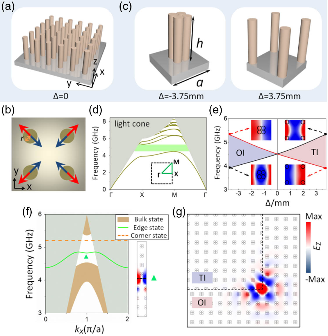
    Figure 1.(a) Schematic of the PCS with Δ=0. The radius and height of cylinders are r and h, respectively, and a metal plate is placed at the bottom. (b) A unit cell of PCS in (a). The blue and red arrows represent the moving direction of the cylinder. (c) 3D diagram of a unit cell with Δ=3.75  mm (left) and Δ=3.75  mm (right); (d) band structure for PCS with Δ=±3.75  mm (inset shows the Brillouin zone). For different signs of Δ, the PCS is in a different topological phase. (e) The evolution of the lowest two bands at X point with Δ and topological phase diagram. The black and red curves represent mirror symmetric and antisymmetric modes, respectively, and the two modes are reversed at Δ=0. Insets, electric field distributions (polarized in the z direction) of the eigenstates at Δ=±3.75  mm. (f) Projected band structure for the combined PCSs of OI (Δ=3.75  mm) and TI (Δ=3.75  mm); the green curve represents the edge state, and the orange dashed line represents the topological corner state with a frequency of 5.17 GHz in the corner structure of (g). Right inset shows the field distribution of edge state when kx=π/a (marked by the green triangle). (g) The simulated electric field distribution of the topological corner state with a frequency of 5.17 GHz; the interface of OI and TI is indicated by the black dashed lines, and a source is placed at the corner of the interface.

    Here, we calculate the band structure for TM polarization of the two PCSs with Δ=3.75  mm and 3.75  mm, as shown in Fig. 1(d). The two PCSs have the same band structure, and we can get a full bandgap (green shadow) in the range of 4.53 to 5.33 GHz between the first and second bands, but the topological phases are different for the two PCSs. To prove this, the evolution of the lowest two bands at the X point with the parameter Δ is shown in Fig. 1(e). It is found that a degenerate point appears when Δ=0 at X point, and the degenerate point is opened when Δ0. Figure 1(e) shows the lowest two bands with different symmetries are reversed when the sign of Δ changes, which indicates that a topological phase transition occurs. Therefore, PCS is in a trivial phase and is a photonic ordinary insulator (OI) when Δ<0. PCS is in a nontrivial phase and is a photonic TI when Δ>0 [6,7]. The different topological properties ensure the existence of edge states along the interface between OI and TI. Here, the projected band diagram of lattices formed by OI and TI PCSs is given, as shown in Fig. 1(f). It is found that there is an edge state (represented by green curve) in the bandgap, and the edge state in the light cone is the resonant leaky mode. The electric field distribution of the edge state at kx=π/a (indicated by a green triangle) is shown in the right inset of Fig. 1(f); the field is localized at the interface of two PCSs. From the projected band diagram, we can also see that there is a bandgap between the edge state and the upper bulk state, and a topological corner state exists in the bandgap. We consider a combined OI-TI (OT) structure, which is composed of an 8×8 period TI surrounded by four layers of OI, and the interface between OI and TI is indicated by black dashed lines in the Fig. 1(g). By calculating the eigenstate of the structure, a corner state with 5.17 GHz [marked by the orange dashed line in the Fig. 1(f)] is found in the bandgap. We then place an excitation source with a frequency of 5.17 GHz at the corner (the intersection of two interfaces) for the full wave simulation. The field distribution shows clearly that most of the energy of the corner state is localized on a single dielectric cylinder at the corner in Fig. 1(g). In Appendix A, we use the topological index to explain the generation of the topological corner state [6,43].

    Next, we investigate the CESs and corner states in ordinary-topological-ordinary (OTO) sandwiched structure. (The counterparts of topological-ordinary-topological (TOT) sandwiched structure are also shown in Appendix B.) One unit of schematic diagram for the OTO structure is shown in Fig. 2(a), and the number of TI units is denoted by N. The parameters of TI and OI regions are the same as those of Fig. 1(d). In the sandwiched structure, there are two interfaces between OI and TI lattices, which are represented by two black dashed lines. We know that the topological edge state decays exponentially away from the OT interface [shown in the inset of Fig. 1(f)], so when the number of TI units is large enough, the two interfaces can be regarded infinitely far apart, and each interface can support an isolated topological edge state. However, when N decreases, the two edge states will couple due to the closeness of the two interfaces, and the two CESs are formed in the bandgap. Here, we give the projected bands of N=3 (left panel), 2 (middle panel), 1 (right panel), as depicted in Fig. 2(b). There are two bands (represented by red and blue curves) in the bandgap, which correspond to the two CESs. The coupling becomes stronger with the decrease of N from 3 to 1; when N=1, the coupling is the strongest, and we can control the dispersions and bandwidth of the CESs by changing N. When N>12, the two CESs emerge into one due to weak coupling, which is almost the same as that of Fig. 1(f). In addition, the bandgap is unchanged when changing N, and almost the same as that of two-phase structure in Fig. 1(f).

    (a) Schematic diagram of OTO sandwiched structure. The number of TI units is denoted by N, and there are two interfaces (represented by dashed black lines) between the OI and TI domains. (b) Projected band structure of OTO PCSs with N=3 (left), 2 (middle), 1 (right); in the OTO bending structure [shown as Fig. 3(a)], the topological corner state (represented by the orange dashed line) always exists, but two CCSs (represented by blue and red dashed lines) appear only when N=1. Top insets, the field distributions of CESs marked by the blue and red triangles.

    Figure 2.(a) Schematic diagram of OTO sandwiched structure. The number of TI units is denoted by N, and there are two interfaces (represented by dashed black lines) between the OI and TI domains. (b) Projected band structure of OTO PCSs with N=3 (left), 2 (middle), 1 (right); in the OTO bending structure [shown as Fig. 3(a)], the topological corner state (represented by the orange dashed line) always exists, but two CCSs (represented by blue and red dashed lines) appear only when N=1. Top insets, the field distributions of CESs marked by the blue and red triangles.

    In the projected band structure of Fig. 2(b), the blue and red curves are used to represent the two CESs, and the EZ field distributions of two CESs at kx=π/a (indicated by red and blue triangles) with different N are shown in the top inset of Fig. 2(b). Based on the EZ field symmetry about the x axis, the two CESs are classified as the antisymmetric (red line) and symmetric (blue line) CESs, respectively. The different symmetries of CESs result from different ways of coupling: in-phase coupling leads the symmetric CES, and anti-phase coupling leads the antisymmetric CES. In addition, symmetric and antisymmetric CESs are reversed with changing N. When N is odd, the antisymmetric CES (red curve) is the high-frequency branch. In contrast, when N is even, the symmetric CES (blue curve) is the higher one. N can control both the coupling strength and the mode symmetry, and it can be used to design the multifunctional photonic crystal waveguides. Therefore, the sandwiched structure hosting CESs, including OTO and TOT (seen in Appendix B), is more flexible compared with the existing OT structure.

    Then, in order to observe the two CESs experimentally, we fabricate a sample consisting of OTO bend as shown in Fig. 3(a), and the black dashed line indicates the center of the TI domain. The material of dielectric cylinders is alumina ceramics with a relative dielectric permittivity of ε=9.4, and the cylinders are fixed on an aluminum plate. The parameters of OI and TI are the same as those of Fig. 2, and the number N of TI unit is one. As shown in Fig. 2(b), when N=1 (right panel), the frequency range of antisymmetric CES is from 4.79 to 5.10 GHz, so we select the working frequency 4.86 GHz to excite the antisymmetric CES, and the excitation source at the bottom of the sample, which is indicated by a red star in the bottom inset of Fig. 3(a). It should be noted that considering the mode distribution of the antisymmetric CES, the position of source should deviate from the center line (indicated by the black dashed line), so that the source can excite the antisymmetric CES. The simulated |E|2 and EZ field distribution are shown in the left panel of Fig. 3(b). We can see that CES is well localized on the two interfaces of OI and TI, and the inset (EZ field distribution) shows the phases are opposite at two interfaces, which is the same as that of Fig. 2(b). By using the near-field scanner, we measure the |E|2 and EZ field distributions, as shown in the right panel of Fig. 3(b). A microwave-emitting antenna is placed at the bottom of the aluminum plate as an excitation source. The probe antenna of the near-field scanning platform moves horizontally on the surface of the sample, and is connected to a Keysight N5224B vector network analyzer to acquire the transmitted magnitude and phase of microwave signals. It is seen that the experimental results are consistent with the simulations. The light flow is localized near the interfaces and propagates with the antisymmetric mode. Similarly, the frequency range of the symmetric CES is from 4.03 to 4.59 GHz, as shown in Fig. 2(b), so we set the frequency of the source to be 4.55 GHz to excite the symmetric CES. The simulated |E|2 field distribution is shown in the left panel of Fig. 3(c), and the inset (EZ field distribution) shows the phases are identical at two interfaces, which is the same as that of Fig. 2(b). The experimental measurement results of field distributions are shown in the right panel of Fig. 3(c), which agrees well with the simulation. Compared with the protected edge state in the existing OT structure [6,7], the CESs in the sandwiched structure feature a high capacity for photonic flow transport.

    (a) Photograph of the experimental OTO bending structure with N=1. The black dashed line represents the center line of the TI domain; an aluminum plate is placed at the bottom. The bottom inset shows the location of the excitation source (red star). (b) The field distribution |E|2 (EZ field distribution in the inset) of the antisymmetric CES in simulation (left panel) and experiment (right panel); the frequency of source is 4.86 GHz; (c) field distribution |E|2 (EZ field distribution in the inset) of the symmetric CES in simulation (left panel) and experiment (right panel); the frequency of source is 4.55 GHz.

    Figure 3.(a) Photograph of the experimental OTO bending structure with N=1. The black dashed line represents the center line of the TI domain; an aluminum plate is placed at the bottom. The bottom inset shows the location of the excitation source (red star). (b) The field distribution |E|2 (EZ field distribution in the inset) of the antisymmetric CES in simulation (left panel) and experiment (right panel); the frequency of source is 4.86 GHz; (c) field distribution |E|2 (EZ field distribution in the inset) of the symmetric CES in simulation (left panel) and experiment (right panel); the frequency of source is 4.55 GHz.

    Because the corner-induced filling abnormally leads to fractional charge, the OTO bending structure also has topological corner state (also seen in Appendix A). By eigenmode calculations, the higher-order topological state at around 5.17 GHz [denoted by the orange dashed line in Fig. 2(b)] is always found with different N, which is almost the same as that of the OT corner structure [shown in Fig. 1(f)]. In addition, we can see from Fig. 2(b) that in all the projected band structures for different N, N=1 is the most noteworthy. Different from others, there is a complete bandgap between the two CESs due to strong coupling when N=1. By eigenmode calculations of the OTO bend, we also find that there are two corner states in the bandgap, located around 4.66 and 4.74 GHz, and indicated by red and blue dashed lines in the right panel of Fig. 2(b), respectively. The two corner states exist accompanied by CESs, so we name them CCSs. We will verify the existence of the topological corner state and CCSs in the OTO bend by experiment below.

    In experiment, the excitation source should be placed at the black dot position (this position should be the nondiagonal position of the bend to excite all three corner states), shown in Fig. 4(a). In order to visualize the evolution of various states with frequency, we use the probe at different positions to detect the bulk (brown), coupled edge (blue), coupled corner and topological corner (red) states’ responses, as shown in Fig. 4(a). In the frequency ranging from 4.3 to 5.4 GHz, the measured spectra of the three probes are shown in Fig. 4(b), where high values mean the existence of eigenstates and low values mean the presence of a bandgap. The spectra clearly indicate the edge and corner (including topological and coupled) modes appearing in the bandgap. It is found that the symmetric CES has a narrow range of response around 4.55 GHz, while there is a continuous response of the antisymmetric CES from 4.76 to 5.1 GHz, in good agreement with the dispersions of the CESs in Fig. 2(b) (right panel). Moreover, the spectrum obtained by the corner probe [indicated by the red dot in Fig. 4(a)] clearly shows three sharp and strong peaks, which correspond to the three corner states denoted by the dashed lines in the right panel of Fig. 2(b). In the gap between symmetric and asymmetric CESs, there are two peaks at around 4.66 and 4.74 GHz, respectively, which correspond to CCSs. The third peak is close to 5.17 GHz, indicating the topological corner state. Here we give the simulated (top) and experimentally measured (bottom) field distributions |E|2 and EZ (inset) of coupled and topological corner states, as shown in Figs. 4(c)–4(e). In Fig. 4(c), it is found that the CCS at 4.66 GHz is antisymmetric about the diagonal line of the corner, but the CCS at 4.74 GHz in Fig. 4(d) is symmetric. So the two CCSs are also classified as the antisymmetric and symmetric CCSs, respectively. Figure 4(e) shows the field distribution of topological corner state is similar to that of Fig. 1(g). All the simulation results agree with experimental measurement results very well. Compared with the existing OT structure [6,7], the two CCSs are also found beside the topological corner state, which enriches the study on the corner states. The experiment results show an evolution of bulk-edge-corner-edge-corner-bulk, which reflects a new hierarchical response of dimensions, and further broadens the research on photonic topological heterostructures.

    (a) Simplified schematic of the experimental OTO bend structure in Fig. 3(a). The excitation source is marked by a black dot, and the brown, blue, and red probes represent the detection of bulk, coupled edge, and corner (including topological and coupled corner) states, respectively. (b) The measured spectra for the probes at the three different positions; the frequencies of the three strongest peaks of corner spectrum are 4.66, 4.74, and 5.17 GHz. (c)–(e) The simulated (top) and experimentally measured (bottom) |E|2 and EZ (inset) field distributions of (c) antisymmetric CCS with a frequency of 4.66 GHz; (d) symmetric CCS with a frequency of 4.74 GHz; (e) topological corner state with a frequency of 5.17 GHz.

    Figure 4.(a) Simplified schematic of the experimental OTO bend structure in Fig. 3(a). The excitation source is marked by a black dot, and the brown, blue, and red probes represent the detection of bulk, coupled edge, and corner (including topological and coupled corner) states, respectively. (b) The measured spectra for the probes at the three different positions; the frequencies of the three strongest peaks of corner spectrum are 4.66, 4.74, and 5.17 GHz. (c)–(e) The simulated (top) and experimentally measured (bottom) |E|2 and EZ (inset) field distributions of (c) antisymmetric CCS with a frequency of 4.66 GHz; (d) symmetric CCS with a frequency of 4.74 GHz; (e) topological corner state with a frequency of 5.17 GHz.

    Further, we compare the localization of coupled and topological corner states by calculating the mode area [44], Sm=ε(r)|E(r)|2d2rmax{ε(r)|E(r)|2},m=1,2,3,where ε(r) is the relative permittivity of the medium at the spatial position r, E(r) is the electric field, and m=1,2,3 indicates the antisymmetric CCS, the symmetric CCS, and the topological corner state, respectively. We get S1=1.44×10⁴  m2, S2=2.65×10⁴  m2, and S3=4.84×10⁵m2. Thus, S1/S3=2.97, and S2/S3=5.47. The smaller mode area indicates the stronger localization; therefore, the topological corner state is better than CCSs in localization. Additionally, Appendix C shows the degenerate corner states of the box structure, which also verify that the topological corner state has better local characteristics than CCSs.

    Finally, we introduce defects to numerically verify the robustness of topological and coupled corner states. We mainly study two types of defects: disordered dielectric cylinders and removed dielectric cylinders. We consider placing an excitation source near the corner for the simulation, as in Fig. 4(a). For the first type of defect, we move the dielectric cylinders near the corner and at the corner, respectively, as shown in Figs. 5(a) and 5(b). For the second type of defect, we remove some cylinders at the outer interface between OI and TI, as depicted in Fig. 5(c). For the two CCSs and the topological corner state, the excitation frequencies of the three corner states are 4.66, 4.74, and 5.17 GHz, respectively. The simulated field distributions are shown in Fig. 5, which are almost the same as those of Figs. 4(c)–4(e), and the results demonstrate that both topological and CCSs are robust against defects and disorders. In addition, we calculate the frequencies of eigenstates for the three corner states by introducing the defects of Fig. 5 and find the offsets of frequencies are very small (all less than 0.02 GHz), which also shows that the three corner states have strong robustness.

    (a), (b) Schematics of the sample with a shift of one cylinder and |E|2 field distributions of three corner states; the red cylinder moves 3 mm along the (a) y direction and (b) both the x and −y directions. (c) Schematics of the sample with a removal of cylinders and |E|2 field distributions of three corner states; the defect positions are indicated by the blue boxes.

    Figure 5.(a), (b) Schematics of the sample with a shift of one cylinder and |E|2 field distributions of three corner states; the red cylinder moves 3 mm along the (a) y direction and (b) both the x and y directions. (c) Schematics of the sample with a removal of cylinders and |E|2 field distributions of three corner states; the defect positions are indicated by the blue boxes.

    3. CONCLUSIONS

    In conclusion, we theoretically investigate the CESs and the three corner states in a proposed OTO sandwiched structure, and visualize these states experimentally by using the near-field scanning technique based on pure dielectric PCSs. Compared with topological edge states in a two-phase structure, the CESs have more diverse symmetries and a high capacity of energy flow. The CCSs can be found in the gap between the two CESs. The multiple corner states, including topological and CCSs, are all robust to defects, which have broad application prospects and can promote the development of integrated photon devices [45,46]. Although our research is carried out at a microwave frequency, the results can also be realized at optical frequency by micronanomachining [47]. In addition, we believe that coupled states exist not only in photonic systems and expect to observe a similar effect in other systems, such as phonon and electron systems.

    APPENDIX A: PRIMITIVE GENERATOR AND TOPOLOGICAL INDEX

    In general, the classification of Cn-symmetric topological crystalline insulators (TCIs) with the rotation representation forms a free Abelian additive structure, which means that the topological class of any given Cn-symmetric TCI can be obtained by a set of primitive generators. For our photonic crystal (PC), the primitive generator is h1b(4), shown in Fig. 6(a). The primitive generator is Wannier-representable, with the Wannier center pinned by symmetry to maximal Wyckoff positions, as shown in Fig. 6(b) (blue and red dots). For C4 symmetry, the energy eigenstates of the Bloch Hamiltonian at high symmetry points (HSPs) in the first Brillouin zone are also eigenstates of the fourfold rotation operator, and the eigenvalues at HSPs Π is Πp=e2πi(p1)/4,p=1,2,3,4,where p represents the different rotation representation, and Π indicate HSPs Γ, X, and M.

    (a) Maximal Wyckoff positions of C4-symmetric unit cell; (b) primitive generator of our topological photonic crystal.

    Figure 6.(a) Maximal Wyckoff positions of C4-symmetric unit cell; (b) primitive generator of our topological photonic crystal.

    The topological corner state arises from a filling anomaly that is caused by the mismatch between the number of particles required and crystal symmetry, which can be described by the topological index constructed by the primitive generator. Based on the rotation eigenvalues at HFCs Π, the bulk polarization and corner topological index are defined as follows: Px=Py=[X1],Qcorner=([X1]+2[M1]+3[M2]),where [Πp]=#Πp#Γp and #Πp is the number of bands below the bandgap with rotation eigenvalues Πp. For primitive generator h1b(4), we have [X1]=1, [M1]=1, and [M2]=0. Thus, P=(Px,Py)=(12,12), which characterizes the topological edge state, and Qcorner=14, indicating that in the topological nontrivial structure (TI), there is a one-quarter fractionalized corner charge, i.e., a topological corner state in both the OT and OTO structures.

    APPENDIX B: CHARACTERISTICS OF THE TOT STRUCTURE

    In addition to the OTO PCSs mentioned in the main text, there is another kind of sandwiched structure, i.e., TOT PCSs. The schematic diagram of TOT structure is shown in Fig. 7(a). The parameters of OI and TI domains are the same as those of OTO, and the number of OI units is denoted by M. In this section, we study the band characteristics of the TOT structure, and in Figs. 7(b)–7(d) we give the projected band when M is 3, 2, and 1, respectively. Similar to OTO, TOT also produces two CESs in the bulk bandgap with different symmetries. The state that is mirror-symmetric about the x direction is represented by a blue curve, and the state that is mirror-antisymmetric is represented by a red curve. When M decreases, the coupling between the edge states at the two interfaces becomes strong. In the top inset of Figs. 7(b)–7(d), we show the field distributions of the two bands in the bandgap at kx=π/a (marked by red and blue triangles) with different M.

    (a) Schematic diagram of TOT sandwiched structure; the number of OI units is denoted by M; (b)–(d) projected band diagram of TOT PCSs with (b) M=3, (c) M=2, and (d) M=1. The frequency of the topological corner state is indicated by the orange dashed line. The top insets show the field distributions EZ of the two states (red and blue curves) at kx=π/a. The simulated field distribution |E|2 of topological corner state with (e) M=2 and (f) M=1 in the OTO corner structure.

    Figure 7.(a) Schematic diagram of TOT sandwiched structure; the number of OI units is denoted by M; (b)–(d) projected band diagram of TOT PCSs with (b) M=3, (c) M=2, and (d) M=1. The frequency of the topological corner state is indicated by the orange dashed line. The top insets show the field distributions EZ of the two states (red and blue curves) at kx=π/a. The simulated field distribution |E|2 of topological corner state with (e) M=2 and (f) M=1 in the OTO corner structure.

    Moreover, the topological corner state always exists in TOT bend structure [as shown in Figs. 7(b)–7(d)], and the frequency is indicated by the orange dashed line in the projected band diagram. But, the CCSs are not found because there is no bandgap between the two CESs. With the decrease of M, the frequency of the topological corner state is almost unchanged compared with that of OT (around 5.17 GHz). We conduct the full wave simulation to verify the topological corner state with frequency 5.17 GHz and give the simulated field distribution |E|2 in Figs. 7(e) and 7(f) with M=2 and 1, respectively. The two interfaces between OI and TI domains are marked by green dashed lines. It is found that the topological corner state is always localized on the inner corner of the constructed structure.

    APPENDIX C: MORE SIMULATED FIELDS OF TOPOLOGICAL AND CCSs IN A BOX-SHAPED OTO STRUCTURE

    In this section, we investigate the topological and CCSs in a box-shaped OTO structure. The parameters of TI and OI regions are the same as those of Fig. 3. It is found there are four degenerate states for both topological and CCSs, respectively, by eigenstate calculations, which originate from the finite size effect.

    When the size of a box-shaped OTO structure is 22×22 periods (the periods of OI/TI/OI are 10, 1, 5 from inside to outside, respectively), we find that the four degenerate topological corner states (around 5.17 GHz) can form multipoles, including one monopole, two dipoles, and one quadrupole [shown as Fig. 8(a) from left to right, respectively]. The similar results of the degenerate CCSs are not shown in order to avoid repetition. When the size of a box-shaped OTO structure is 26×26 periods (the periods of OI/TI/OI are 14, 1, 5 from inside to outside, respectively), we find that the four degenerate antisymmetric and symmetric CCSs (around 4.74 and 4.66 GHz) can form multipoles, including one monopole, two dipoles, and one quadrupole [shown in Figs. 8(b) and 8(c) from left to right, respectively]. But the four degenerate topological corner states (around 5.17 GHz) cannot form multipoles, as shown in Fig. 8(d). The topological corner state has better local characteristics than CCSs, which is verified in the main text. So, when the size of a box-shaped OTO structure is 26×26 periods, the CCSs at the four corners can be coupled with each other, and the multipoles can be achieved, but the topological corner state cannot. In addition, we consider a larger-size structure with 30×30 periods (the periods of OI/TI/OI are 18, 1, 5 from inside to outside, respectively). The simulated fields of the three kinds of corner states (with a frequency of 4.74, 4.66, and 5.17 GHz from left to right, respectively) are shown in Fig. 8(e). Here, we only give one of the four degenerate states, and it is found that the CCSs and topological corner states are all isolated at one corner, respectively. The coupling between the neighboring corners disappears and multipoles for CESs and the topological corner state do not exist at all when the size of the box is large enough.

    (a) EZ fields of four degenerate eigenmodes of the topological corner state (around 5.17 GHz) in the box-shaped OTO structure with 22×22 periods; EZ fields of four degenerate eigenmodes of (b), (c) two CCSs (around 4.66 and 4.74 GHz) and (d) topological corner state (around 5.17 GHz) in the box-shaped OTO structure with 26×26 periods; (e) EZ fields of one eigenmode of the three corner states (with a frequency of 4.74, 4.66, and 5.17 GHz from left to right, respectively) in a larger-sized metastructure with 30×30 periods, which verifies that there is no coupling among the corners when the size is large enough.

    Figure 8.(a) EZ fields of four degenerate eigenmodes of the topological corner state (around 5.17 GHz) in the box-shaped OTO structure with 22×22 periods; EZ fields of four degenerate eigenmodes of (b), (c) two CCSs (around 4.66 and 4.74 GHz) and (d) topological corner state (around 5.17 GHz) in the box-shaped OTO structure with 26×26 periods; (e) EZ fields of one eigenmode of the three corner states (with a frequency of 4.74, 4.66, and 5.17 GHz from left to right, respectively) in a larger-sized metastructure with 30×30 periods, which verifies that there is no coupling among the corners when the size is large enough.

    References

    [1] D. J. Thouless, M. Kohmoto, M. P. Nightingale, M. den Nijs. Quantized Hall conductance in a two-dimensional periodic potential. Phys. Rev. Lett., 49, 405-408(1982).

    [2] F. D. M. Haldane, S. Raghu. Possible realization of directional optical waveguides in photonic crystals with broken time-reversal symmetry. Phys. Rev. Lett., 100, 013904(2008).

    [3] D. Hsieh, D. Qian, L. Wray, Y. Xia, Y. S. Hor, R. J. Cava, M. Z. Hasan. A topological Dirac insulator in a quantum spin Hall phase. Nature, 452, 970-974(2008).

    [4] X. L. Qi, S. C. Zhang. Topological insulators and superconductors. Rev. Mod. Phys., 83, 1057-1110(2011).

    [5] Z. Wang, Y. Chong, J. D. Joannopoulos, M. Soljacic. Observation of unidirectional backscattering-immune topological electromagnetic states. Nature, 461, 772-775(2009).

    [6] B. Y. Xie, G. X. Su, H. F. Wang, H. Su, X. P. Shen, P. Zhan, M. H. Lu, Z. L. Wang, Y. F. Chen. Visualization of higher-order topological insulating phases in two-dimensional dielectric photonic crystals. Phys. Rev. Lett., 122, 233903(2019).

    [7] X. D. Chen, W. M. Deng, F. L. Shi, F. L. Zhao, M. Chen, J. W. Dong. Direct observation of corner states in second-order topological photonic crystal slabs. Phys. Rev. Lett., 122, 233902(2019).

    [8] A. B. Khanikaev, S. H. Mousavi, W. K. Tse, M. Kargarian, A. H. MacDonald, G. Shvets. Photonic topological insulators. Nat. Mater., 12, 233-239(2013).

    [9] J. Noh, W. A. Benalcazar, S. Huang, M. J. Collins, K. P. Chen, T. L. Hughes, M. C. Rechtsman. Topological protection of photonic mid-gap defect modes. Nat. Photonics, 12, 408-415(2018).

    [10] X. Huang, Y. Lai, Z. H. Hang, H. Zheng, C. T. Chan. Dirac cones induced by accidental degeneracy in photonic crystals and zero-refractive-index materials. Nat. Mater., 10, 582-586(2011).

    [11] L. H. Wu, X. Hu. Scheme for achieving a topological photonic crystal by using dielectric material. Phys. Rev. Lett., 114, 223901(2015).

    [12] C. He, X. Ni, H. Ge, X. C. Sun, Y. B. Chen, M. H. Lu, X. P. Liu, Y. F. Chen. Acoustic topological insulator and robust one-way sound transport. Nat. Phys., 12, 1124-1129(2016).

    [13] X. Ni, M. Weiner, A. Alù, A. B. Khanikaev. Observation of higher-order topological acoustic states protected by generalized chiral symmetry. Nat. Mater., 18, 113-120(2019).

    [14] Z. J. Yang, F. Gao, X. Lin, B. L. Zhang. Topological acoustics. Phys. Rev. Lett., 114, 114301(2015).

    [15] M. Xiao, G. C. Ma, Z. Y. Yang, P. Sheng, Z. Q. Zhang, C. T. Chan. Geometric phase and band inversion in periodic acoustic systems. Nat. Phys., 11, 240-244(2015).

    [16] H. L. He, C. Y. Qiu, L. P. Ye, X. Y. Fan, M. Z. Ke, Z. Y. Liu. Topological negative refraction of surface acoustic waves in a Weyl phononic crystal. Nature, 560, 61-64(2018).

    [17] Y. T. Yang, Y. F. Xu, T. Xu, X. Hu, Z. H. Hang. Visualization of a unidirectional electromagnetic waveguide using topological photonic crystals made of dielectric materials. Phys. Rev. Lett., 120, 217401(2018).

    [18] Y. Poo, R. X. Wu, Z. Lin, Y. Yang, C. T. Chan. Experimental realization of self-guiding unidirectional electromagnetic edge states. Phys. Rev. Lett., 106, 093903(2011).

    [19] X. Ni, C. He, X. C. Sun, X. P. Liu, M. H. Lu, L. Feng, Y. F. Chen. Topologically protected one-way edge mode in networks of acoustic resonators with circulating air flow. New J. Phys., 17, 053016(2015).

    [20] G. C. Wei, Z. Z. Liu, Y. C. Liu, D. S. Zhang, J. J. Xiao. Frequency selective topological edge wave routing in meta-structures made of cylinders. Opt. Lett., 45, 5608-5611(2020).

    [21] J. F. Chen, W. Y. Liang, Z. Y. Li. Broadband dispersionless topological slow light. Opt. Lett., 45, 4964-4967(2020).

    [22] H. Y. Zhang, L. Qian, C. Y. Wang, C. C. Lu. Topological rainbow based on graded topological photonic crystals. Opt. Lett., 46, 1237-1240(2021).

    [23] W. A. Benalcazar, B. A. Bernevig, T. L. Hughes. Quantized electric multipole insulators. Science, 357, 61-66(2017).

    [24] C. W. Peterson, W. A. Benalcazar, T. L. Hughes, G. Bahl. A quantized microwave quadrupole insulator with topologically protected corner states. Nature, 555, 346-350(2018).

    [25] Z. D. Song, Z. Fang, C. Fang. (D−2)-dimensional edge states of rotation symmetry protected topological states. Phys. Rev. Lett., 119, 246402(2017).

    [26] M. Geier, L. Trifunovic, M. Hoskam, P. W. Brouwer. Second-order topological insulators and superconductors with an order-two crystalline symmetry. Phys. Rev. B, 97, 205135(2018).

    [27] H. D. Xue, Y. H. Yang, F. Gao, Y. D. Chong, B. L. Zhang. Acoustic higher-order topological insulator on a Kagome lattice. Nat. Mater., 18, 108-112(2019).

    [28] X. J. Zhang, H. X. Wang, Z. K. Lin, Y. Tian, B. Y. Xie, M. H. Lu, Y. F. Chen, J. H. Jiang. Second-order topology and multidimensional topological transitions in sonic crystals. Nat. Phys., 15, 582-588(2019).

    [29] D. Xiao, M. C. Chang, Q. Niu. Berry phase effects on electronic properties. Rev. Mod. Phys., 82, 1959-2007(2010).

    [30] T. L. Hughes, R. G. Leigh, O. Parrikar. Torsional anomalies, Hall viscosity, and bulk-boundary correspondence in topological states. Phys. Rev. D, 88, 025040(2013).

    [31] C. Han, M. Kang, H. Jeon. Lasing at multidimensional topological states in a two-dimensional photonic crystal structure. ACS Photon., 7, 2027-2036(2020).

    [32] X. T. He, M. Y. Li, H. Y. Qiu, F. L. Zhao, J. W. Dong. In-plane excitation of a topological nanophotonic corner state at telecom wavelengths in a cross-coupled cavity. Photon. Res., 9, 1423-1431(2019).

    [33] C. Schmidt, A. Palatnik, M. Sudzius, K. Leo. Coupled topological interface states. Phys. Rev. B, 103, 085412(2021).

    [34] M. D. Wang, W. Y. Zhou, L. Y. Bi, C. Y. Qiu, M. Z. Ke, Z. Y. Liu. Valley-locked waveguide transport in acoustic heterostructures. Nat. Commun., 11, 3000(2020).

    [35] Q. L. Chen, L. Zhang, F. J. Chen, H. S. Chen, Y. H. Yang. Photonic topological valley-locked waveguides. ACS Photon., 8, 1400-1406(2021).

    [36] M. L. N. Chen, L. J. Jiang, Z. Lan, W. E. I. Sha. Pseudospin-polarized topological line defects in dielectric photonic crystals. IEEE Trans. Antennas Propag., 68, 609-613(2020).

    [37] Y. F. Gao, Z. Jiang, L. L. Zhang, L. He, J. Zhao. Unidirectional propagation of coupled edge states in sandwich topological photonic crystals. J. Appl. Phys., 124, 213107(2018).

    [38] Z. Jiang, Y. F. Gao, L. He, H. Song, J. Zhou, R. J. Zhu. Helical edge states of topological photonic crystals with line defects. Appl. Opt., 58, 2294-2299(2019).

    [39] W. P. Su, J. R. Schrieffer, A. J. Heeger. Solitons in polyacetylene. Phys. Rev. Lett., 42, 1698-1701(1979).

    [40] F. Liu, K. Wakabayashi. Novel topological phase with a zero Berry curvature. Phys. Rev. Lett., 118, 076803(2017).

    [41] F. Liu, H. Y. Deng, K. Wakabayashi. Topological photonic crystals with zero Berry curvature. Phys. Rev. B, 97, 035442(2018).

    [42] C. Poli, M. Bellec, U. Kuhl, F. Mortessagne, H. Schomerus. Selective enhancement of topologically induced interface states in a dielectric resonator chain. Nat. Commun., 6, 6710(2015).

    [43] W. A. Benalcazar, T. Li, T. L. Hughes. Quantization of fractional corner charge in CN-symmetric higher-order topological crystalline insulators. Phys. Rev. B, 99, 245151(2019).

    [44] X. D. Yang, J. Yao, X. Zhang. Experimental realization of three-dimensional indefinite cavities at the nanoscale with anomalous scaling laws. Nat. Photonics, 6, 450-454(2012).

    [45] M. Yoshida, M. De Zoysa, K. Ishizaki, Y. Tanaka, M. Kawasaki, R. Hatsuda, B. Song, J. Gelleta, S. Noda. Double-lattice photonic-crystal resonators enabling high-brightness semiconductor lasers with symmetric narrow divergence beams. Nat. Mater., 18, 121-128(2019).

    [46] F. Alpeggiani, L. Kuipers. Topological edge states in bichromatic photonic crystals. Optica, 6, 96-103(2019).

    [47] M. Campbell, D. N. Sharp, M. T. Harrison, R. G. Denning, A. J. Turberfield. Fabrication of photonic crystals for the visible spectrum by holographic lithography. Nature, 404, 53-56(2000).

    Mingxing Li, Yueke Wang, Tian Sang, Hongchen Chu, Yun Lai, Guofeng Yang. Experimental observation of multiple edge and corner states in photonic slabs heterostructures[J]. Photonics Research, 2022, 10(1): 197
    Download Citation