
Gengxin Chen, Ziliang Ruan, Zong Wang, Pucheng Huang, Changjian Guo, Daoxin Dai, Kaixuan Chen, Liu Liu, "Four-channel CWDM device on a thin-film lithium niobate platform using an angled multimode interferometer structure," Photonics Res. 10, 8 (2022)
- Photonics Research
- Vol. 10, Issue 1, 8 (2022)
Abstract
1. INTRODUCTION
In the last decades, the photonic integrated circuit (PIC) has attracted much research interest, and enables integration of active and passive optical components on a single chip in a scalable manner. Numerous PIC platforms, such as silicon-on-insulator (SOI) [1], silicon nitride (SiN) [2], and indium phosphate (InP) [3], have been widely explored for photonic integration. Lithium niobate (LN), due to its wide transparent window, strong electro-optic (EO) effect, large nonlinear optical coefficient, and chemical stability, has been widely used in making various kinds of active optical components. Traditional waveguides on bulk LN are typically fabricated using technologies of titanium diffusion or proton exchange, which leads to an indistinct waveguide boundary and small index contrast between the waveguide core and its cladding regions [4]. Therefore, optical components fabricated on bulk LN are usually large, and high density integration is considered not feasible on this material platform. Recently, thin-film LN (TFLN) [5] has attracted a lot of attention due to its capability to support sub-micrometer-sized waveguides on LN, which can then lead to compact optical components as compared to those on bulk LN. Ultra-low-loss TFLN waveguides using a dry etching technique [6] have already been demonstrated. Therefore, TFLN is considered as one of the most promising PIC platforms for future optical communications.
Due to the aforementioned large EO coefficient of LN, high-speed EO modulators on a TFLN platform, such as phase modulators [7], Mach–Zehnder modulators [8,9], Michelson interferometer modulators [10], and in-phase/quadrature modulators [11], have shown excellent performance as compared to their counterparts on other PIC platforms, such as SOI. As TFLN can simultaneously confine optical and acoustic modes, waveguide-based acousto-optic modulators working at sub-gigahertz acoustic frequencies have been demonstrated [12] based on suspended TFLN waveguides. Due to the large nonlinear optical coefficient and low linear waveguide losses, ultra-high-efficiency wavelength conversion with a normalized conversion efficiency of
Although a number of studies on active TFLN devices have been reported, there are still many passive devices worth exploring, such as wavelength-division multiplexing (WDM) devices. Combining WDM technology and high-performance EO modulators [14], multi-channel, multi-wavelength transmitter chips, which are important components for data-center optical communications, can then be built on TFLN [15,16]. As LN is an anisotropic material, TFLN waveguides exhibit unique mode properties as compared to waveguides based on conventional isotropic materials [17]. It has been shown that significant polarization coupling related to mode hybridization through a waveguide bend can be observed. This has become the dominant factor limiting the compactness of on-chip routing for TFLN waveguides. Therefore, WDM devices using conventional structures such as array-waveguide gratings (AWGs) [18], planar concave gratings (PCGs) [19], and cascading Mach–Zehnder interferometers (CMZIs) [20] are difficult to design on the TFLN platform. Recently, a CWDM device using a multimode waveguide grating structure [21] on a hybrid platform consisting of TFLN and silicon rich nitride has been demonstrated at C-band. However, this structure is incompatible with state-of-the-art high-speed EO modulators on the monolithic TFLN platform discussed here. In this paper, we demonstrate a coarse WDM (CWDM) device based on an angled multimode interferometer (MMI) structure on the TFLN platform. The key part of the proposed device is essentially a straight multimode waveguide without involving any bending structures. Although CWDM devices using an angled MMI structure have been demonstrated on SOI and SiN platforms [22,23], implementations of such a structure, as well as efficient CWDM structures in general, on the TFLN platform are still missing. The proposed device here can support ultra-low insertion losses and cross talks for four supported wavelength channels, and can be adopted for CWDM transmitters at O-band.
Sign up for Photonics Research TOC. Get the latest issue of Photonics Research delivered right to you!Sign up now
2. DEVICE DESIGN AND PRINCIPLE
Figure 1(a) shows the schematic layout of the proposed four-channel CWDM device on TFLN. The basic structure consists of a multimode dispersive waveguide, i.e., the angled MMI of width
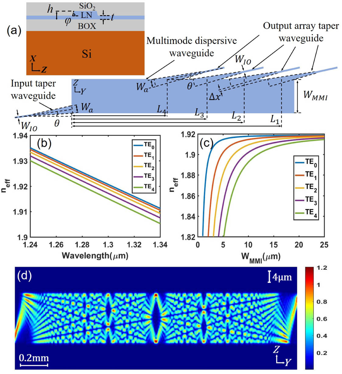
Figure 1.(a) Schematic diagram of the four-channel CWDM on TFLN based on an angled MMI structure. (b) Calculated wavelength dependence of the
The channel spacing
Optimized Structural Parameters for the Four-Channel CWDM Device on TFLN
| Channel # | 1 | 2 | 3 | 4 |
| 1271 | 1291 | 1311 | 1331 | |
| 2054 | 2017 | 1980 | 1943 | |
One can find that the minimal line width of the proposed design is
![]()
Figure 2.Simulated spectral responses of the proposed CWDM device with different tilted angles: (a)
![]()
Figure 3.Simulated spectral responses of the proposed CWDM device for (a)
The fabrication tolerance of the proposed CWDM device is also studied. The spectral responses of channel #1 with different
![]()
Figure 4.Simulated fabrication tolerance of the proposed CWDM device with changes (a) in
3. DEVICE FABRICATION AND MEASUREMENT
The designed angled MMI based four-channel CWDM device with parameters shown in Table 1 was then fabricated on a wafer (NanoLN) consisting of a 400 nm thick
![]()
Figure 5.(a) Microscope image of a fabricated device. Scanning electron microscope images of (b) input coupling grating, (c) input waveguide, (d) output waveguides, and (e) output coupling gratings.
![]()
Figure 6.(a) Schematic of the measurement setup. (b) Measured spectral response of the fabricated CWDM device. (c) Measured peak wavelength positions (red dots), linear fit (red dotted line), and simulated peak wavelength positions (blue dots) for channel #1 with variations in
4. CONCLUSION
In conclusion, we have demonstrated a four-channel CWDM device on the TFLN platform using an angled MMI structure. The key part of the proposed device is simply a straight multimode waveguide. This avoids using bent waveguides needed in other types of CWDM structures, whose radius is extraordinarily large in anisotropic planar structures such as TFLN [17]. The overall footprint of the proposed device is about 2.1 mm × 0.02 mm. Ultra-low insertion losses of
References
[1] B. Jalali, S. Fathpour. Silicon photonics. J. Lightwave Technol., 24, 4600-4615(2006).
[2] J. David, M. Roberto, L. Alexander, L. Michal. New CMOS-compatible platforms based on silicon nitride and Hydex for nonlinear optics. Nat. Photonics, 7, 597-607(2013).
[3] R. Nagarajan, M. Kato, D. Lambert, P. Evans, S. Corzine, V. Lal, J. Rahn, A. Nilsson, M. Fisher, M. Kuntz, J. Pluemeekers, A. Dentai, H. S. Tsai, D. Krause, H. Sun, K. Wu, M. Ziari, T. Butrie, M. Reffle, M. Mitchell, F. Kish, D. Welch. Terabits class InP photonic integrated circuits. Semicond. Sci. Technol., 27, 094003(2012).
[4] Y. Qi, Y. Li. Integrated lithium niobate photonics. Nanophotonics, 9, 1287-1320(2020).
[5] D. Zhu, L. Shao, M. Yu, R. Cheng, B. Desiatov, C. Xin, Y. Hu, J. Holzgrafe, S. Ghosh, A. Shams-Ansari, E. Puma, N. Sinclair, C. Reimer, M. Zhang, M. Loncar. Integrated photonics on thin-film lithium niobate. Adv. Opt. Photon., 13, 242-352(2021).
[6] I. Krasnokutska, J. L. J. Tambasco, X. Li, A. Peruzzo. Ultra-low loss photonic circuits in lithium niobate on insulator. Opt. Express, 26, 897-904(2018).
[7] T. Ren, M. Zhang, C. Wang, L. Shao, C. Reimer, Y. Zhang, O. King, R. Esman, T. Cullen, M. Loncar. An integrated low-voltage broadband lithium niobate phase modulator. IEEE Photon. Technol. Lett., 31, 889-892(2019).
[8] C. Wang, M. Zhang, X. Chen, M. Bertrand, A. Shams-Ansari, S. Chandrasekhar, P. Winzer, M. Loncar. Integrated lithium niobate electro-optic modulators operating at CMOS-compatible voltages. Nature, 562, 101-104(2018).
[9] M. He, M. Xu, Y. Ren, J. Jian, Z. Ruan, Y. Xu, S. Gao, S. Sun, X. Wen, L. Zhou, L. Liu, C. Guo, H. Chen, S. Yu, L. Liu, X. Cai. High-performance hybrid silicon and lithium niobate Mach-Zehnder modulators for 100 Gbit s–1 and beyond. Nat. Photonics, 13, 359-364(2019).
[10] J. Jian, M. Xu, L. Liu, Y. Luo, J. Zhang, L. Liu, L. Zhou, H. Chen, S. Yu, X. Cai. High modulation efficiency lithium niobate Michelson interferometer modulator. Opt. Express, 27, 18731-18739(2019).
[11] M. Xu, M. He, H. Zhang, J. Jian, Y. Pan, X. Liu, L. Chen, X. Meng, H. Chen, Z. Li, X. Xiao, S. Yu, X. Cai. High-performance coherent optical modulators based on thin-film lithium niobate platform. Nat. Commun., 11, 3911(2020).
[12] L. Shao, M. Yu, S. Maity, N. Sinclair, L. Zheng, C. Chia, A. Shams-Ansari, C. Wang, M. Zhang, K. Lai, M. Loncar. Microwave-to-optical conversion using lithium niobate thin-film acoustic resonators. Optica, 6, 1498-1505(2019).
[13] A. Rao, K. Adbelsalam, T. S. Aardema, A. Honardoost, G. F. Camacho-Gonzalez, S. Fathpour. Actively-monitored periodic-poling in thin-film lithium niobate photonic waveguides with ultrahigh nonlinear conversion efficiency of 4600% W–1 cm–2. Opt. Express, 27, 25920-25930(2019).
[14] J. Cai, C. Guo, C. Lu, A. Lau, P. Chen, L. Liu. Design optimization of silicon and lithium niobate hybrid integrated traveling-wave Mach-Zehnder modulator. IEEE Photon. J., 13, 2200206(2021).
[15] C. Zhang, S. Zhang, J. Peters, J. Bowers. 8×8×40 Gbps fully integrated silicon photonic network on chip. Optica, 3, 785-786(2016).
[16] J. Hu, C. Li, C. Guo, C. Lu, A. Lau, P. Chen, L. Liu. Folded thin-film lithium niobate modulator based on a poled Mach–Zehnder interferometer structure. Opt. Lett., 46, 2940-2943(2021).
[17] J. Wang, P. Chen, D. Dai, L. Liu. Polarization coupling of
[18] P. Pan, J. An, Y. Wang, J. Zhang, L. Wang. Compact 4-channel AWGs for CWDM and LAN WDM in data center monolithic applications. Opt. Laser Technol., 75, 177-181(2015).
[19] S. Pathak, P. Dumon, D. V. Thourhout, W. Bogaerts. Comparison of AWGs and Echelle gratings for wavelength division multiplexing on silicon-on-insulator. IEEE Photon. J., 6, 4900109(2014).
[20] H. Xu, Y. Shi. Flat-top CWDM (de)multiplexer based on MZI with bent directional couplers. IEEE Photon. Technol. Lett., 30, 169-172(2018).
[21] Y. Liu, X. Huang, H. Guan, Z. Yu, Q. Wei, Z. Fan, W. Han, Z. Li. C-band four-channel CWDM (de-)multiplexers on a thin film lithium niobate–silicon rich nitride hybrid platform. Opt. Lett., 46, 4726-4729(2021).
[22] Y. Hu, R. Jenkins, F. Gardes, E. Finlayson, G. Mashanovich, G. Reed. Wavelength division (de)multiplexing based on dispersive self-imaging. Opt. Lett., 36, 4488-4490(2011).
[23] T. Bucio, A. Khokhar, G. Mashanovich, F. Gardes. N-rich silicon nitride angled MMI for coarse wavelength division (de)multiplexing in the O-band. Opt. Lett., 43, 1251-1254(2018).
[24] P. Kharel, C. Reimer, K. Luke, L. He, M. Zhang. Breaking voltage–bandwidth limits in integrated lithium niobate modulators using micro-structured electrodes. Optica, 8, 357-363(2021).
[25] D. Liu, M. Zhang, Y. Shi, D. Dai. Four-channel CWDM (de)multiplexers using cascaded multimode waveguide gratings. IEEE Photon. Technol. Lett., 32, 192-195(2020).
[26] G. Gao, D. Chen, S. Tao, Y. Zhang, S. Zhu, X. Xiao, J. Xia. Silicon nitride O-band (de)multiplexers with low thermal sensitivity. Opt. Express, 25, 12260-12267(2017).
[27] G. F. R. Chen, J. W. Choi, E. Sahin, D. K. T. Ng, D. T. H. Tan. On-chip 1 by 8 coarse wavelength division multiplexer and multi-wavelength source on ultra-silicon-rich nitride. Opt. Express, 27, 23549-23557(2019).
[28] L. Shen, H. Wang, C. Xu, W. Huang. Numerical analysis of multimode interference effect in Ti:LiNbO3 waveguides. Proc. SPIE, 5970, 59700W(2005).
[29] Z. Ruan, Y. Zhu, P. Chen, Y. Shi, S. He, X. Cai, L. Liu. Efficient hybrid integration of long-wavelength VCSELs on silicon photonic circuits. J. Lightwave Technol., 38, 5100-5106(2020).


Set citation alerts for the article
Please enter your email address

© Copyright 2018-2021 | Chinese Laser Press. All Rights Reserved 沪ICP备15018463号-20