
Shihan Hong, Long Zhang, Yi Wang, Ming Zhang, Yiwei Xie, Daoxin Dai, "Ultralow-loss compact silicon photonic waveguide spirals and delay lines," Photonics Res. 10, 1 (2022)
- Photonics Research
- Vol. 10, Issue 1, 1 (2022)
Abstract
1. INTRODUCTION
Loss reduction is considered as the most fundamental and critical priority in the development of on-chip photonic integrated circuits (PICs), and tremendous efforts have been made to develop ultralow-loss optical waveguides in the past decades. Many PICs used for true-time-delay lines [1–6], optical gyroscopes [7,8], optical coherence tomography [9,10], and microwave photonics beam-forming [11,12] often require very long on-chip waveguides, and hence various low-loss optical waveguides have been demonstrated on different platforms such as
Basically speaking, currently there are two typical methods to reduce the scattering losses in optical waveguides. One is to smoothen the waveguide sidewalls (characterized by the mean square deviation
In this paper, we propose and realize an ultralow-loss and ultra-compact 220-nm-thick silicon strip waveguide spiral fabricated with standard MPW processes. Here the silicon strip waveguide is designed with a broadened core region beyond the single-mode regime. In this way, the field amplitude at the sidewalls can be reduced significantly, and thus the scattering loss is reduced greatly. Particularly, to be compact with negligible losses as well as high-order mode excitation, a tapered Euler-curve S-bend is introduced for the waveguide spiral. With such low-loss and compact waveguide spirals, a 10-bit tunable optical true-time-delay line on silicon is realized with a time delay as long as 5120 ps for the first time.
2. STRUCTURE AND DESIGN
Figure 1(a) shows the configuration of the proposed silicon photonic waveguide spiral, which consists of single-mode input/output waveguides, two bent waveguide tapers, two multimode Archimedean spiral waveguides, and a tapered Euler-curve S-bend in the middle. The bent waveguide tapers should be long enough to adiabatically connect the narrow input/output waveguide and the broadened Archimedean spiral waveguide, so that the fundamental-mode loss and the higher-order mode excitation ratio is negligible. Usually, the length of the bent waveguide tapers is chosen as
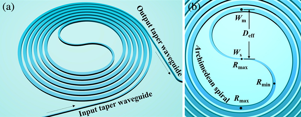
Figure 1.(a) 3D view of the proposed ultralow-loss and compact silicon photonic waveguide spiral. (b) Enlarged view of tapered Euler-curve S-bend in the middle.
To evaluate the loss due to the scattering at the waveguide interfaces, which is the major loss source, a three-dimensional volume current method was used for modeling [26–28]. In this way, the scattering is modeled as an equivalent polarization volume current density. Figures 2(a)–2(c) show the calculated losses due to the top/bottom surface scattering and sidewall scattering, as well as the total scattering loss, respectively. Apparently, the scattering loss decreases greatly as the roughness
![]()
Figure 2.Calculated losses due to the (a) top/bottom surface scattering (here
For standard MPW processes, the sidewall roughness
As another key factor to minimize the footprint of the waveguide spiral, the gap width
![]()
Figure 3.Calculated coupling length
As is well known, the design of a broadened waveguide bend should be careful to avoid excitation of the higher-order mode when light carried by the fundamental mode propagates along the multimode waveguide spiral. Notice that the S-bend in the middle is one of the keys for the waveguide spiral design because there is an abrupt change of the bending radii from
Figures 4(a) and 4(b) show the calculated excess loss and intermode cross talk as the radius
![]()
Figure 4.(a) Calculated excess loss and (b) intermode cross talk as a function of the core width
Figures 4(c) and 4(e) show the simulated light propagation in the designed tapered Euler-curve S-bend and the calculated mode-excitation ratios monitored at the output port. Here a three-dimensional finite-difference time-domain (3D-FDTD) method was used in the simulation. From Fig. 4(c), it can be seen that the launched
3. FABRICATION AND CHARACTERIZATION
The designed silicon photonic waveguide spirals were fabricated by the MPW foundry (Institute of Microelectronics, China) with the standard processes of deep UV lithography and inductively coupled plasma dry-etching. A 1-μm-thick silica thin film was deposited on the top as the upper-cladding. There are seven samples of chips, and each has five waveguide spirals with different lengths of
Figure 5(a) shows the microscope image of the fabricated 50-cm-long silicon photonic waveguide spiral. The setup with an amplified spontaneous emission (ASE) source and an optical spectrum analyzer (OSA) was used for measuring the transmissions of these waveguide spirals. Here grating couplers were used for efficient chip–fiber coupling. The measured transmissions in the wavelength range of 1530–1580 nm are shown in Fig. 5(b). It can be seen that the waveguide loss is almost wavelength insensitive in the C-band, which indicates that there is no multimode interference occurring in the waveguide spirals. The measured waveguide losses at 1550 nm for seven chips are given in Fig. 5(c). It can be seen that the waveguide loss increases linearly with propagation distance. The data fitting shows the measured waveguide loss is about
![]()
Figure 5.(a) Microscope image of the fabricated 50-cm-long waveguide spiral. (b) Measured transmissions of the waveguide spirals with different lengths
The present waveguide spirals are further used to develop an
![]()
Figure 6.(a) Schematic configuration of the
Table 1 gives a summary of on-chip tunable optical delay lines reported up to now. In particular, here only broadband time-delay lines are taken into account. Owing to the strong mode confinement, the propagation loss of regular silicon photonic waveguide spirals is usually as high as 2–3 dB/cm [1,5], which can be reduced to 0.6 dB/cm by introducing special thin silicon photonic waveguides or to 0.9 dB/cm by shallow etching to ridge-type waveguides as demonstrated in Refs. [3,4]. In contrast, our proposed silicon waveguide spiral has a propagation as low as 0.28 dB/cm and a minimal bending radius as compact as 10 μm, which makes it possible to realize a long time delay (e.g., 5.12 ns), a high resolution (e.g., 10 ps), as well as a compact footprint (e.g.,
Performance Comparison of On-Chip Tunable Delay Lines Based on Silicon-on-Insulator Waveguides
| Reference | Waveguide (WG) Type | Bit | Delay Tuning | Resolution | Loss | Footprint |
|---|---|---|---|---|---|---|
| [ | Subwavelength grating silicon WG ( | 1 | 181.9 | 4.7 | 2.6 | 56.55 |
| [ | Ridge WG ( | 7 | 191.37 | 1.42 | 2.47 | 13.32 |
| [ | Thin silicon WG ( | 7 | 1280 | Small (BW = 0.48 nm) | 0.6 | 28.62 |
| [ | Ridge Si WG ( | 7 | 1270 | 10 | 0.9 | 11.84 |
| This work | Broadened silicon WG ( | 10 | 5110 | 10 | 0.28 | 12.98 |
4. CONCLUSION
In summary, we have proposed and demonstrated a novel silicon photonic waveguide spiral consisting of single-mode input/output waveguides, two bent waveguide tapers, two broadened Archimedean spiral waveguides, and a tapered Euler-curve S-bend in the middle. The core width of the Archimedean spiral waveguides is chosen optimally to be
References
[1] Y. Wang, H. Sun, M. Khalil, W. Dong, I. Gasulla, J. Capmany, L. R. Chen. On-chip optical true time delay lines based on subwavelength grating waveguides. Opt. Lett., 46, 1405-1408(2021).
[2] R. L. Moreira, J. Garcia, W. Li, J. Bauters, J. S. Barton, M. J. R. Heck, J. E. Bowers, D. J. Blumenthal. Integrated ultra-low-loss 4-bit tunable delay for broadband phased array antenna applications. IEEE Photon. Technol. Lett., 25, 1165-1168(2013).
[3] J. Xie, L. Zhou, Z. Li, J. Wang, J. Chen. Seven-bit reconfigurable optical true time delay line based on silicon integration. Opt. Express, 22, 22707-22715(2014).
[4] X. Wang, L. Zhou, R. Li, J. Xie, L. Lu, K. Wu, J. Chen. Continuously tunable ultra-thin silicon waveguide optical delay line. Optica, 4, 507-515(2017).
[5] P. Zheng, C. Wang, X. Xu, J. Li, D. Lin, G. Hu, R. Zhang, B. Yun, Y. Cui. A seven bit silicon optical true time delay line for Ka-band phased array antenna. IEEE Photon. J., 11, 5501809(2019).
[6] H. Sun, Y. Wang, L. R. Chen. Integrated discretely tunable optical delay line based on step-chirped subwavelength grating waveguide Bragg gratings. J. Lightwave Technol., 38, 5551-5560(2020).
[7] B. Wu, Y. Yu, J. Xiong, X. Zhang. Silicon integrated interferometric optical gyroscope. Sci. Rep., 8, 8766(2018).
[8] S. Gundavarapu, M. Belt, T. A. Huffman, M. A. Tran, T. Komljenovic, J. E. Bowers, D. J. Blumenthal. Interferometric optical gyroscope based on an integrated Si3N4 low-loss waveguide coil. J. Lightwave Technol., 36, 1185-1191(2018).
[9] G. Yurtsever, B. Považay, A. Alex, B. Zabihian, W. Drexler, R. Baets. Photonic integrated Mach-Zehnder interferometer with an on-chip reference arm for optical coherence tomography. Biomed. Opt. Express, 5, 1050-1061(2014).
[10] X. Ji, X. Yao, Y. Gan, A. Mohanty, M. A. Tadayon, C. P. Hendon, M. Lipson. On-chip tunable photonic delay line. APL Photon., 4, 090803(2019).
[11] C. Zhu, L. Lu, W. Shan, W. Xu, G. Zhou, L. Zhou, J. Chen. Silicon integrated microwave photonic beamformer. Optica, 7, 1162-1170(2020).
[12] P. Zheng, X. Xu, D. Lin, P. Liu, G. Hu, B. Yun, Y. Cui. A wideband 1×4 optical beam-forming chip based on switchable optical delay lines for Ka-band phased array. Opt. Commun., 488, 126842(2021).
[13] J. F. Bauters, M. J. R. Heck, D. D. John, J. S. Barton, C. M. Bruinink, A. Leinse, R. G. Heideman, D. J. Blumenthal, J. E. Bowers. Planar waveguides with less than 0.1 dB/m propagation loss fabricated with wafer bonding. Opt. Express, 19, 24090-24101(2011).
[14] H. Lee, T. Chen, J. Li, O. Painter, K. J. Vahala. Ultra-low-loss optical delay line on a silicon chip. Nat. Commun., 3, 867(2012).
[15] K. K. Lee, D. R. Lim, L. C. Kimerling, J. Shin, F. Cerrina. Fabrication of ultralow-loss Si/SiO2 waveguides by roughness reduction. Opt. Lett., 26, 1888-1890(2001).
[16] J. Cardenas, C. B. Poitras, J. T. Robinson, K. Preston, L. Chen, M. Lipson. Low loss etchless silicon photonic waveguides. Opt. Express, 17, 4752-4757(2009).
[17] D. K. Sparacin, S. J. Spector, L. C. Kimerling. Silicon waveguide sidewall smoothing by wet chemical oxidation. J. Lightwave Technol., 23, 2455-2461(2005).
[18] F. Gao, Y. Wang, G. Cao, X. Jia, F. Zhang. Improvement of sidewall surface roughness in silicon-on-insulator rib waveguides. Appl. Phys. B, 81, 691-694(2005).
[19] C. Bellegarde, E. Pargon, C. Sciancalepore, C. Petit-Etienne, V. Hugues, D. Robin-Brosse, J.-M. Hartmann, P. Lyan. Improvement of sidewall roughness of submicron SOI waveguides by hydrogen plasma and annealing. IEEE Photon. Technol. Lett., 30, 591-594(2018).
[20] P. Dong, W. Qian, S. Liao, H. Liang, C. C. Kung, N. N. Feng, R. Shafiiha, J. Fong, D. Feng, A. V. Krishnamoorthy, M. Asghari. Low loss shallow-ridge silicon waveguides. Opt. Express, 18, 14474-14479(2010).
[21] W. Bogaerts, L. Chrostowski. Silicon photonics circuit design: methods, tools and challenges. Laser Photon. Rev., 12, 1700237(2018).
[22] D. Dai. Advanced passive silicon photonic devices with asymmetric waveguide structures. Proc. IEEE, 106, 2117-2143(2018).
[23] D. Thomson, A. Zilkie, J. E. Bowers, T. Komljenovic, G. T. Reed, L. Vivien, D. Marris-Morini, E. Cassan, L. Virot, J.-M. Fédéli, J.-M. Hartmann, J. H. Schmid, D.-X. Xu, F. Boeuf, P. O’Brien, G. Z. Mashanovich, M. Nedeljkovic. Roadmap on silicon photonics. J. Opt., 18, 073003(2016).
[24] Y. Vlasov, S. McNab. Losses in single-mode silicon-on-insulator strip waveguides and bends. Opt. Express, 12, 1622-1631(2004).
[25] S. Suzuki, M. Yanagisawa, Y. Hibino, K. Oda. High-density integrated planar lightwave circuits using SiO2-GeO2 waveguides with a high refractive index difference. J. Lightwave Technol., 12, 790-796(1994).
[26] T. Barwicz, H. A. Haus. Three-dimensional analysis of scattering losses due to sidewall roughness in microphotonic waveguides. J. Lightwave Technol., 23, 2719-2732(2005).
[27] C. Ciminelli, V. M. N. Passaro, F. Dell’Olio, M. N. Armenise. Three-dimensional modelling of scattering loss in InGaAsP/InP and silica-on-silicon bent waveguides. J. Eur. Opt. Soc., 4, 09015(2009).
[28] J. F. Bauters, M. J. Heck, D. John, D. Dai, M. C. Tien, J. S. Barton, A. Leinse, R. G. Heideman, D. J. Blumenthal, J. E. Bowers. Ultra-low-loss high-aspect-ratio Si3N4 waveguides. Opt. Express, 19, 3163-3174(2011).
[29] C. Qiu, F. Gan, Z. Sheng, H. Li, W. Liu, L. Li, A. Pang, A. Wu, X. Wang, S. Zou. Fabrication, characterization and loss analysis of silicon nanowaveguides. J. Lightwave Technol., 32, 2303-2307(2014).
[30] K. K. Lee, D. R. Lim, H.-C. Luan, A. Agarwal, J. Foresi, L. C. Kimerling. Effect of size and roughness on light transmission in a Si/SiO2 waveguide: experiments and model. Appl. Phys. Lett., 77, 1617-1619(2000).
[31] T. Barwicz, H. I. Smith. Evolution of line-edge roughness during fabrication of high-index-contrast microphotonic devices. J. Vac. Sci. Technol. B, 21, 2892(2003).
[32] L. B. Soldano, E. C. M. Pennings. Optical multi-mode interference devices based on self-imaging: principles and applications. J. Lightwave Technol., 13, 615-627(1995).
[33] X. Jiang, H. Wu, D. Dai. Low-loss and low-crosstalk multimode waveguide bend on silicon. Opt. Express, 26, 17680-17689(2018).
[34] L. Zhang, L. Jie, M. Zhang, Y. Wang, Y. Xie, Y. Shi, D. Dai. Ultrahigh-
[35] M. Cherchi, S. Ylinen, M. Harjanne, M. Kapulainen, T. Aalto. Dramatic size reduction of waveguide bends on a micron-scale silicon photonic platform. Opt. Express, 21, 17814-17823(2013).
[36] L. Song, H. Li, D. Dai. Mach-Zehnder silicon-photonic switch with low random phase errors. Opt. Lett., 46, 78-81(2021).
[37] S. Liu, A. Khope. Latest advances in high-performance light sources and optical amplifiers on silicon. J. Semicond., 42, 041307(2021).
[38] C. Liu, J. Guo, L. Yu, J. Li, M. Zhang, H. Li, Y. Shi, D. Dai. Silicon/2D-material photodetectors: from near-infrared to mid-infrared. Light Sci. Appl., 10, 123(2021).
[39] Y. Zhao, X. Wang, D. Gao, J. Dong, X. Zhang. On-chip programmable pulse processor employing cascaded MZI-MRR structure. Front. Optoelectron., 12, 148-156(2018).
[40] H. Wang, H. Chai, Z. Lv, Z. Zhang, L. Meng, X. Yang, T. Yang. Silicon photonic transceivers for application in data centers. J. Semicond., 41, 101301(2020).


Set citation alerts for the article
Please enter your email address

© Copyright 2018-2021 | Chinese Laser Press. All Rights Reserved 沪ICP备15018463号-20