
Shaonan Zheng, Hong Cai, Linfang Xu, Nanxi Li, Zhonghua Gu, Yao Zhang, Weiguo Chen, Yanyan Zhou, Qingxin Zhang, Lennon Yao Ting Lee, "Silicon substrate-integrated hollow waveguide for miniaturized optical gas sensing," Photonics Res. 10, 261 (2022)
- Photonics Research
- Vol. 10, Issue 1, 261 (2022)
Abstract
1. INTRODUCTION
Gas sensors have drawn significant interest from academic research to commercial applications [1–6]. Among various existing gas sensing technologies [7–15], optical gas sensors based on the interaction between photons and chemical gas molecules stand out for their high sensitivity, high selectivity, long life time, short response time, and long-term operation stability [16–20]. Many important gases have characteristic absorption lines in the mid-infrared (MIR) range (2–12 μm) [21], allowing high-selectivity and high-sensitivity detection. Hence, MIR sensors are highly desirable for increasing needs in various application scenarios. A conventional hollow waveguide (HWG) is widely used in transmitting IR light in a wide spectral range from 0.9 to 25 μm with low loss (0.5–1.5 dB/m at 10.6 μm) thanks to a dielectric layer as the inner coating of the metallic waveguide surface [22,23]. Various gas sensing and spectroscopic applications have been demonstrated exploiting an HWG with tens of centimeters to several meters coupled to spectrometer or laser to enable high sensitivity (down to ppb-level detection limit) [24–28]. However, conventional HWG is unsuitable for compact gas sensor due to its high cost and susceptibility to mechanical vibration and shock. Substrate-integrated HWGs (iHWGs) are emerging as a promising technology recently for gas sensing and spectroscopy [29,30]. They are fabricated into a mechanically robust substrate with small footprint to dramatically release the influence of mechanical vibration and shock. In Ref. [29], a 21.8 cm long spiral iHWG with average loss of 2.32 dB/mm is developed and tested on an optical alignment system for sensing of several gases using a Fourier transform infrared (FTIR) spectrometer and HgCdTe (MCT) detector. A low limit of detection (LOD) of 21 ppm (parts per million) is achieved for
In comparison with solid-core waveguides, iHWG suffers from higher optical loss due to larger surface roughness and sensitivity to bending, hindering its applications, which requires ultralow detection limit (sub-ppm level). However, solid-core waveguide sensing in the MIR range is limited by its alignment tolerance with the light source and detector, which is due to the waveguide dimensions (hundreds of nanometers to a few micrometers). In the meanwhile, iHWG with much larger waveguide dimensions (a few hundred micrometers) allows direct free-space light coupling and significantly larger alignment tolerance with the light source and detector. Hence, the iHWG is viable for a chemical gas sensor working in the MIR wavelength range for applications requiring ppm-level detection limit.
To address the increasing needs of compact and low-cost gas sensors [4,21], in this work, the iHWGs fabricated into silicon wafer substrate are developed and experimentally demonstrated for chemical gas sensing. The demonstrated compact iHWGs are fabricated on an 8-inch (200 mm) standard silicon wafer for chemical gas sensing. By leveraging silicon wafer-scale etching and bonding processes, the Si-iHWG sensors can be mass-produced. Hence, the cost can be dramatically reduced compared with the iHWGs built into a metal substrate. Further, we experimentally demonstrated a fully functional compact nondispersive infrared (NDIR)
Sign up for Photonics Research TOC. Get the latest issue of Photonics Research delivered right to you!Sign up now
2. DESIGN AND WORKING PRINCIPLE
The schematic of a spiral iHWG formed on silicon wafer substrate (bottom wafer) is shown in Fig. 1(a). The Si-iHWG in an optical gas sensing system acts as both the optical waveguide and gas cell. The spiral path is designed to realize larger path length for higher sensitivity while maintaining a small footprint. The physical length of the spiral Si-iHWG is 34.07 mm. The bending radius is 2.2 mm. Figure 1(b) shows the schematic of the cross section. The designed semicircle radius is 250 μm. It is formed with one flat-top wafer and one etched-bottom wafer. The inner surfaces of both wafer substrates are coated with a reflective metallic film. Here, gold film is chosen as the reflective metallic film. In this work, the Si-iHWG chip is assembled with the off-chip light-emitting diode (LED, AKM AK9700AE) and photodetector (PD, AKM AK9710AEF01) by a specially designed holder to build an NDIR
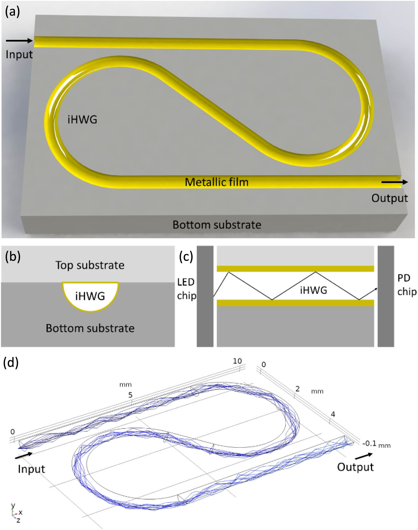
Figure 1.(a) Schematic of a spiral iHWG etched on a silicon wafer substrate. (b) Cross section of the spiral iHWG. (c) Schematic assembly of LED, Si-iHWG, and PD. Drawings in (a)–(c) are not to scale. (d) Ray trajectory simulation in the spiral Si-iHWG. The source rays are the rays at 15° (angle between light ray and the
Based on Beer–Lambert law, with a monochromatic light source, the transmittance is expressed as
Figure 1(d) shows the ray trajectory simulation in the spiral Si-iHWG. The source rays are the ones at 15° (angle between the light ray and
3. EXPERIMENTAL SECTION
A. Fabrication of Si-iHWG
Figure 2 shows the fabrication process of Si-iHWG with a semicircular cross section. The drawing is not to scale. It starts with two 8-inch (200 mm) silicon wafers, one as the bottom wafer for Si-iHWG formation and the other as the top covering wafer to form the top part of the Si-iHWG. For the bottom wafer, a dense gold film is firstly deposited as a hard mask through the sputtering process, which is wet etched later using potassium iodide solution. The silicon substrate is thereafter wet etched to obtain a smooth semicircular cross-sectional shape. Afterwards, the gold hard mask is removed, and a 300 nm thick gold film is deposited uniformly as the reflection layer through evaporation. Gold film is chosen due to its high reflectivity (99.5%) near wavelength of 4 μm [41] and suitability for wafer bonding. The top wafer is firstly etched by DRIE followed by silicon isotropic etching to form funnel-shaped blind holes. Then back grinding is performed to form funnel-shaped through holes. Thereafter, another 300 nm thick gold film is deposited uniformly on the surface as the reflection layer through evaporation. Such gold film deposition is done as the last step in order to avoid any particle contamination that could impact the inner surface reflection. The thin wafer after back-grinding is handled by temporarily hosting it on a supporting silicon wafer for further process. Finally, the 8-inch (200 mm) top wafer and the bottom wafer are bonded together at 300°C with 3 kN force for 2.5 h to form the Si-iHWG.
![]()
Figure 2.Fabrication process of Si-iHWG with a semicircular cross section. Drawing is not to scale. Two silicon wafers are used, one as the bottom wafer for Si-iHWG formation and the other as the top covering wafer to form the top part of the Si-iHWG. The top wafer and the bottom wafer are bonded together to form the Si-iHWG.
Figure 3(a) shows the optical micrograph of a Si-iHWG chip consisting of a straight Si-iHWG and a spiral Si-iHWG. The physical lengths of the straight and spiral Si-iHWGs are 10 mm and 34.07 mm, respectively. The chip footprint is
![]()
Figure 3.(a) Optical micrograph of a Si-iHWG chip consisting of a straight Si-iHWG and a spiral Si-iHWG. The chip footprint is
B. Si-iHWG Loss Characterization Setup
Figure 4 shows the schematic of experimental setup for Si-iHWG loss characterization. The Si-iHWG chip is mounted on a six-axis optical fiber alignment system for characterization. The loss measurement is conducted in a normal laboratory environment. A tunable laser (M Squared Firefly IR) is used as the light source. The laser tuning range is from 3294 to 4277 nm. The linewidth is
![]()
Figure 4.Experimental setup for Si-iHWG loss characterization. ZBLAN:
C. Sensor Testing Setup
A fully functional NDIR
![]()
Figure 5.(a) Fully functional NDIR
Figure 6 shows the schematic of experimental setup for
![]()
Figure 6.Gas testing setup. Gas flows from two cylinders are precisely and independently controlled by two mass flow controllers (MFCs). The gas flow rate into sensor inlet is fixed at 500 standard cubic centimeters per minute (SCCM).
4. RESULTS AND DISCUSSIONS
A. Si-iHWG Loss Analysis
Figures 7(a) and 7(b) show the measured propagation loss and coupling loss of the straight Si-iHWG, respectively, in the 35 nm spectral range. Five chips chosen across the same wafer are measured. Each chip consists of a straight Si-iHWG with a different length. The waveguide lengths of 2.5, 4, 5, 5.5, and 7 mm are used for waveguide loss and coupling loss measurement. Due to cross-sectional dimension variations of Si-iHWGs across the whole wafer and variations contributed by manual alignment, the average propagation loss and average coupling loss are extracted and shown as data points in Fig. 7. Please note that the error bars in Figs. 7(a) and 7(b) denote standard deviations of propagation loss from repeated measurements and coupling loss measured from the waveguides with five different lengths, respectively. From the experimental data, propagation loss in the straight Si-iHWG is
![]()
Figure 7.(a) Propagation loss of straight Si-iHWG. (b) Coupling loss between optical fiber and straight Si-iHWG. The error bars in (a) and (b) denote standard deviations of propagation loss from repeated measurements and coupling loss measured from the waveguides with five different lengths, respectively.
To measure the insertion loss, seven identical chips chosen from the same wafer as shown in Fig. 3(a) are tested. The total insertion loss of a straight Si-iHWG (10 mm) and a spiral Si-iHWG (34.07 mm) is measured to be
B. Gas Sensing Analysis
Figure 8(a) shows the detected power, i.e.,
![]()
Figure 8.(a) Output voltage from PD_s and PD_ref while changing
Figure 9(a) shows the sensor response
![]()
Figure 9.(a) Sensor response
5. CONCLUSION
In conclusion, Si-iHWGs are demonstrated for miniaturized gas sensing. The reported Si-iHWGs are formed by wet etching silicon wafer and wafer bonding. The chip footprint consisting of a straight and a spiral Si-iHWGs is
Acknowledgment
Acknowledgment. The authors thank Dr. Doris Keh Ting Ng for discussions. Also, the authors appreciate the fruitful discussions with experts from Robert Bosch (SEA) Pte. Ltd.
References
[1] R. A. Potyrailo. Multivariable sensors for ubiquitous monitoring of gases in the era of internet of things and industrial internet. Chem. Rev., 116, 11877-11923(2016).
[2] H. Yuan, N. Li, J. Linghu, J. Dong, Y. Wang, A. Karmakar, J. Yuan, M. Li, P. J. S. Buenconsejo, G. Liu, H. Cai, S. J. Pennycook, N. Singh, D. Zhao. Chip-level integration of covalent organic frameworks for trace benzene sensing. ACS Sens., 5, 1474-1481(2020).
[3] S. Feng, F. Farha, Q. Li, Y. Wan, Y. Xu, T. Zhang, H. Ning. Review on smart gas sensing technology. Sensors, 19, 3760(2019).
[4] L. Sari, Y. Rafic, A. Yasser, S. Mohamad. Review of recent trends in gas sensing technologies and their miniaturization potential. Sens. Rev., 34, 24-35(2014).
[5] N. Liu, M. L. Tang, M. Hentschel, H. Giessen, A. P. Alivisatos. Nanoantenna-enhanced gas sensing in a single tailored nanofocus. Nat. Mater., 10, 631-636(2011).
[6] H. Yuan, G. Liu, Z. Qiao, N. Li, P. J. S. Buenconsejo, S. Xi, A. Karmakar, M. Li, H. Cai, S. J. Pennycook, D. Zhao. Solution-processable metal–organic framework nanosheets with variable functionalities. Adv. Mater., 33, 2101257(2021).
[7] B. Chocarro-Ruiz, J. Pérez-Carvajal, C. Avci, O. Calvo-Lozano, M. I. Alonso, D. Maspoch, L. M. Lechuga. A CO2 optical sensor based on self-assembled metal–organic framework nanoparticles. J. Mater. Chem. A, 6, 13171-13177(2018).
[8] J. Wu, M. Yin, K. Seefeldt, A. Dani, R. Guterman, J. Yuan, A. P. Zhang, H.-Y. Tam.
[9] H. Yuan, J. Tao, N. Li, A. Karmakar, C. Tang, H. Cai, S. J. Pennycook, N. Singh, D. Zhao. On-chip tailorability of capacitive gas sensors integrated with metal–organic framework films. Angew. Chem., 58, 14089-14094(2019).
[10] M. R. Tchalala, Y. Belmabkhout, K. Adil, K. N. Chappanda, A. Cadiau, P. M. Bhatt, K. N. Salama, M. Eddaoudi. Concurrent sensing of CO2 and H2O from air using ultramicroporous fluorinated metal–organic frameworks: effect of transduction mechanism on the sensing performance. ACS Appl. Mater. Interface, 11, 1706-1712(2019).
[11] H. Yuan, J. Cui, N. Li, M. Li, X. Yu, W. Fan, A. Karmakar, J. Dong, S. J. Pennycook, H. Cai, D. Zhao. On-chip template-directed conversion of metal hydroxides to metal–organic framework films with enhanced adhesion. ACS Appl. Mater. Interface, 12, 36715-36722(2020).
[12] C. Sun, Q. Shi, D. Hasan, M. S. Yazici, M. Zhu, Y. Ma, B. Dong, Y. Liu, C. Lee. Self-powered multifunctional monitoring system using hybrid integrated triboelectric nanogenerators and piezoelectric microsensors. Nano Energy, 58, 612-623(2019).
[13] F. Juang. Ag additive and nanorod structure enhanced gas sensing properties of metal oxide-based CO2 sensor. IEEE Sens. J., 19, 4381-4385(2019).
[14] S. Kanaparthi, S. G. Singh. Chemiresistive sensor based on zinc oxide nanoflakes for CO2 detection. ACS Appl. Nano Mater., 2, 700-706(2019).
[15] N. B. Tanvir, O. Yurchenko, E. Laubender, R. Pohle, O. V. Sicard, G. Urban. Zinc peroxide combustion promoter in preparation of CuO layers for conductometric CO2 sensing. Sens. Actuators B Chem., 257, 1027-1034(2018).
[16] X. Liu, S. Cheng, H. Liu, S. Hu, D. Zhang, H. Ning. A survey on gas sensing technology. Sensors, 12, 9635-9665(2012).
[17] J. Hodgkinson, R. P. Tatam. Optical gas sensing: a review. Meas. Sci. Technol., 24, 012004(2012).
[18] B. Robert. Detecting gases with light: a review of optical gas sensor technologies. Sens. Rev., 35, 133-140(2015).
[19] T.-V. Dinh, I.-Y. Choi, Y.-S. Son, J.-C. Kim. A review on non-dispersive infrared gas sensors: improvement of sensor detection limit and interference correction. Sens. Actuators B Chem., 231, 529-538(2016).
[20] N. Li, H. Yuan, L. Xu, Y. Zeng, B. Qiang, Q. J. Wang, S. Zheng, H. Cai, L. Y. T. Lee, N. Singh, D. Zhao. Tailorable infrared emission of microelectromechanical system-based thermal emitters with NiO films for gas sensing. Opt. Express, 29, 19084-19093(2021).
[21] D. Popa, F. Udrea. Towards integrated mid-infrared gas sensors. Sensors, 19, 2076(2019).
[22] C. M. Charlton, G. Orellana, M. C. Moreno-Bondi, B. T. Thompson, B. Mizaikoff. Hollow waveguide infrared spectroscopy and sensing. Frontiers in Chemical Sensors: Novel Principles and Techniques, 133-167(2005).
[23] P. Patimisco, V. Spagnolo, M. S. Vitiello, G. Scamarcio, C. M. Bledt, J. A. Harrington. Low-loss hollow waveguide fibers for mid-infrared quantum cascade laser sensing applications. Sensors, 13, 1329-1340(2013).
[24] S.-S. Kim, N. Menegazzo, C. Young, J. Chan, C. Carter, B. Mizaikoff. Mid-infrared trace gas analysis with single-pass Fourier transform infrared hollow waveguide gas sensors. Appl. Spectrosc., 63, 331-337(2009).
[25] X. Li, J. Pawlat, J. Liang, T. Ueda. Measurement of low gas concentrations using photonic bandgap fiber cell. IEEE Sens. J., 10, 1156-1161(2010).
[26] N. Liu, J. Sun, H. Deng, J. Ding, L. Zhang, J. Li. Recent progress on gas sensor based on quantum cascade lasers and hollow fiber waveguides. Proc. SPIE, 10250, 102501W(2017).
[27] T. Wu, W. Kong, M. Wang, Q. Wu, W. Chen, C. Ye, R. Hu, X. He. Compact hollow waveguide mid-infrared gas sensor for simultaneous measurements of ambient CO2 and water vapor. J. Lightwave Technol., 38, 4580-4587(2020).
[28] J. Li, G. Luo, Z. Du, Y. Ma. Hollow waveguide enhanced dimethyl sulfide sensor based on a 3.3 μm interband cascade laser. Sens. Actuators B Chem., 255, 3550-3557(2018).
[29] A. Wilk, J. C. Carter, M. Chrisp, A. M. Manuel, P. Mirkarimi, J. B. Alameda, B. Mizaikoff. Substrate-integrated hollow waveguides: a new level of integration in mid-infrared gas sensing. Anal. Chem., 85, 11205-11210(2013).
[30] E. Tütüncü, V. Kokoric, A. Wilk, F. Seichter, M. Schmid, W. E. Hunt, A. M. Manuel, P. Mirkarimi, J. B. Alameda, J. C. Carter, B. Mizaikoff. Fiber-coupled substrate-integrated hollow waveguides: an innovative approach to mid-infrared remote gas sensors. ACS Sens., 2, 1287-1293(2017).
[31] X. Jia, J. Roels, R. Baets, G. Roelkens. On-chip non-dispersive infrared CO2 sensor based on an integrating cylinder. Sensors, 19, 4260(2019).
[32] W. Yang, J. Ferrara, K. Grutter, A. Yeh, C. Chase, Y. Yue, A. E. Willner, M. C. Wu, C. J. Chang-Hasnain. Low loss hollow-core waveguide on a silicon substrate. Nanophotonics, 1, 23-29(2012).
[33] L. Tombez, E. J. Zhang, J. S. Orcutt, S. Kamlapurkar, W. M. J. Green. Methane absorption spectroscopy on a silicon photonic chip. Optica, 4, 1322-1325(2017).
[34] E. J. Zhang, Y. Martin, J. S. Orcutt, C. Xiong, M. Glodde, N. Marchack, E. A. Duch, T. Barwicz, L. Schares, W. M. Green. Monolithically integrated silicon photonic chip sensor for near-infrared trace-gas spectroscopy. Proc. SPIE, 11010, 110100B(2019).
[35] C. Ranacher, C. Consani, A. Tortschanoff, R. Jannesari, M. Bergmeister, T. Grille, B. Jakoby. Mid-infrared absorption gas sensing using a silicon strip waveguide. Sens. Actuators A Phys., 277, 117-123(2018).
[36] C. Ranacher, C. Consani, N. Vollert, A. Tortschanoff, M. Bergmeister, T. Grille, B. Jakoby. Characterization of evanescent field gas sensor structures based on silicon photonics. IEEE Photon. J., 10, 2700614(2018).
[37] P. Su, Z. Han, D. Kita, P. Becla, H. Lin, S. Deckoff-Jones, K. Richardson, L. C. Kimerling, J. Hu, A. Agarwal. Monolithic on-chip mid-IR methane gas sensor with waveguide-integrated detector. Appl. Phys. Lett., 114, 051103(2019).
[38] F. Ottonello-Briano, C. Errando-Herranz, H. Rödjegård, H. Martin, H. Sohlström, K. B. Gylfason. Carbon dioxide absorption spectroscopy with a mid-infrared silicon photonic waveguide. Opt. Lett., 45, 109-112(2020).
[39] S. Zheng, H. Cai, L. Xu, N. Li, J. Fu, Z. Gu, Y. Zhang, W. Chen, Y. Cui, F. M. Kai. Miniaturized gas sensor based on silicon substrate-integrated hollow waveguides. Proc. SPIE, 11689, 116890C(2021).
[40] E. G. Camargo, S. Takehara. Gas sensor. U.S. patent(2020).
[41] S. Babar, J. H. Weaver. Optical constants of Cu, Ag, and Au revisited. Appl. Opt., 54, 477-481(2015).
[42] N. Li, H. Yuan, L. Xu, J. Tao, D. K. T. Ng, L. Y. T. Lee, D. D. Cheam, Y. Zeng, B. Qiang, Q. Wang, H. Cai, N. Singh, D. Zhao. Radiation enhancement by graphene oxide on microelectromechanical system emitters for highly selective gas sensing. ACS Sens., 4, 2746-2753(2019).
[43] D. Jung, S. Bank, M. L. Lee, D. Wasserman. Next-generation mid-infrared sources. J. Opt., 19, 123001(2017).
[44] S. Z. Ali, A. De Luca, R. Hopper, S. Boual, J. Gardner, F. Udrea. A low-power, low-cost infra-red emitter in CMOS technology. IEEE Sens. J., 15, 6775-6782(2015).
[45] N. Li, Q. Chao, Z. Gu, S. Song, Y. Zhou, S. Zheng, L. Xu, Y. Da Chua, Q. Zhang, H. Cai. Photonic crystal MEMS emitter for chemical gas sensing. Proc. SPIE, 11697, 116970M(2021).
[46] B. J. O’Regan, Y. Wang, T. F. Krauss. Silicon photonic crystal thermal emitter at near-infrared wavelengths. Sci. Rep., 5, 13415(2015).
[47] J. Faist, F. Capasso, D. L. Sivco, C. Sirtori, A. L. Hutchinson, A. Y. Cho. Quantum cascade laser. Science, 264, 553-556(1994).
[48] N. Li, E. S. Magden, Z. Su, N. Singh, A. Ruocco, M. Xin, M. Byrd, P. T. Callahan, J. D. B. Bradley, C. Baiocco, D. Vermeulen, M. R. Watts. Broadband 2-μm emission on silicon chips: monolithically integrated holmium lasers. Opt. Express, 26, 2220-2230(2018).
[49] H. Lin, Z. Luo, T. Gu, L. C. Kimerling, K. Wada, A. Agarwal, J. Hu. Mid-infrared integrated photonics on silicon: a perspective. Nanophotonics, 7, 393-420(2017).


Set citation alerts for the article
Please enter your email address

© Copyright 2018-2021 | Chinese Laser Press. All Rights Reserved 沪ICP备15018463号-20