
Xiongliang Wei, Syed Ahmed Al Muyeed, Haotian Xue, Elia Palmese, Renbo Song, Nelson Tansu, Jonathan J. Wierer, "Near-infrared electroluminescence of AlGaN capped InGaN quantum dots formed by controlled growth on photoelectrochemical etched quantum dot templates," Photonics Res. 10, 33 (2022)
- Photonics Research
- Vol. 10, Issue 1, 33 (2022)
Abstract
1. INTRODUCTION
Quantum dot (QD) light emitters have great potential for light-emitting diodes (LEDs) and lasers for end-use applications such as solid-state lighting and displays [1–4]. QDs are synthesized either epitaxially [5,6] or in free-standing, colloidal form [7–10]. Of interest here are epitaxially grown InGaN QDs. Theoretically, QD-based LEDs should have a larger spontaneous emission rate than quantum well (QW) LEDs [11]. Also, QD-based laser diodes should have lower threshold currents due to low carrier thresholds and higher differential gain [12,13]. The benefits of the QD active layer for both LEDs and lasers are mainly due to the strong three-dimensional confinement of electron and holes pairs [14,15], high delta density of states, higher electron and hole wave function overlap, and lower Auger recombination at high carrier densities [4]. There are various electroluminescence (EL) demonstrations of InGaN-based QD LEDs [16–18] and lasers [19,20].
Even though QDs have compelling advantages, InGaN-based QD light emitters have lower efficiencies than QWs because of growth challenges. The traditional method is Stranski–Krastanov (SK) growth, which relies on the spontaneous formation of QDs due to the strain of the underlying growth layers. It is challenging to synthesize InGaN QDs with high dot density and uniform size distribution using SK growth, attributed to the small lattice constant difference between InGaN QDs and GaN [21–24]. Another complication is that SK InGaN QDs are not stable at high temperatures and collapse into GaN barriers via In intermixing or decomposition [25–27] due to strain between the InGaN and GaN. This instability restricts the growth temperatures of subsequent layers, such as GaN barriers. The typical growth temperature of SK InGaN QDs is between 600°C to 800°C [25,28,29], and growth temperatures of subsequent GaN barrier layers are restricted to below 800°C [27,30–32]. This low-temperature GaN will have high defect density and poor morphology, which complicates the growth of multiple QD layers. There is a trade-off between QD integrity and high temperature grown (or higher quality) subsequent layers.
An alternative InGaN QD synthesis method is photoelectrochemical (PEC) etched QDs [33–35]. PEC QDs are formed by etching an InGaN thin film with a laser source. QDs are created from this InGaN layer during etching, and etching ends when the QDs can no longer absorb the laser light. PEC QDs have higher dot density and smaller size variations compared to SK QDs. However, the photoluminescence (PL) of PEC QDs (emission at
Sign up for Photonics Research TOC. Get the latest issue of Photonics Research delivered right to you!Sign up now
It has been shown that instead of using PEC InGaN QDs as the light active layer, they can be used as a template layer for SK InGaN QD growth. SK QDs grown on PEC QD templates can have higher dot density and more controlled size distribution by growing on PEC etched InGaN QD templates due to the lattice strain from the PEC QD layer [36]. This method also avoids exposure of the light-producing QDs. PEC QDs are capped with AlGaN/GaN layers to protect the QDs and planarize the surface to complete the template. These SK QDs are intended as the light-emitting active layer in the LED.
In this work, insights and innovations are applied to SK InGaN QDs grown on PEC QD templates. AlGaN capping layers are employed to prevent collapse via In intermixing or decomposition of InGaN QDs and enable higher GaN barrier growth temperatures [37,38]. This capping scheme removes the trade-off between QD integrity and GaN barrier growth temperature. Different Al-content AlGaN capping layers are studied to protect the SK and PEC QDs against collapse at different GaN barrier growth temperatures. Atomic force microscopy (AFM) and scanning transmission electron microscopy (STEM) show the structure of QDs at various growth steps. These measurements show that high-Al-content
2. EXPERIMENTAL DETAILS
The QD samples are grown by vertical-flow metalorganic chemical vapor deposition (MOCVD), starting with c-plane planar n-type GaN on patterned sapphire substrates at a pressure of 200 Torr (1 Torr = 133.3 Pa). First, to fabricate the PEC QD templates, a 7.5 nm thick
SK QDs are grown by MOCVD on the top of the PEC QD templates with two different Al-content
An SK QD sample with a 2 nm thick
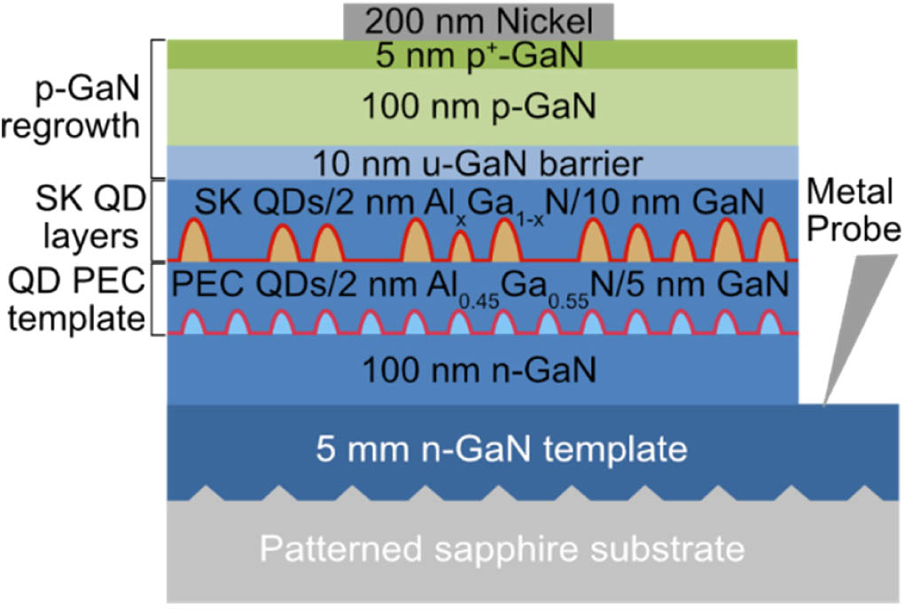
Figure 1.Schematic cross section of the entire LED structure consisting of Stranski–Krastanov (SK) quantum dots (QDs) grown on photoelectrochemical (PEC) etched QD templates. Both QD layers are capped with AlGaN layers to protect the QDs. The p-GaN contact is formed by Ni evaporation through a shadow mask, and an electrical “flash” process creates the n-contact.
3. RESULTS AND DISCUSSION
The integrity of PEC QDs and the eventual template morphology are determined by pausing at each step (PEC etching, AlGaN capping layer growth, and GaN barrier growth) and taking AFM images. Figure 2(a) shows an AFM image of PEC etched QDs over a
![]()
Figure 2.Atomic force microscope (AFM) images of a PEC QD template at different synthesized steps: (a) PEC QDs after etching, (b) PEC QDs with
Next, SK QD samples are grown on top of PEC QD templates. The localized strain caused by PEC QDs in the template layer affects the SK QD size distribution and density [36]. The In and Ga atoms prefer to form on top of the strained area (above the PEC QDs). If the AlGaN/GaN capping layers in the template are too thick, the benefits are lost, and SK QDs grow unaffected by PEC QDs (similar to planar GaN). Figure 3(a) shows an AFM image of SK QDs with an average height of 12 nm and average radius of 40 nm. The dot density is slightly lower than that of the QD template. The SK QD growth temperature employed here is higher than previous reports [36], and there is a dependence of reduced dot density with increasing growth temperature that requires further investigation. The surface between the SK QDs is smooth with no pits, which is different from the PEC QD template surface. This AFM image is an indication that an InGaN wetting layer has covered the GaN surface.
![]()
Figure 3.AFM images of SK QDs grown on a PEC QD template and with
Two different
Figures 3(d) and 3(e) show STEM images of QDs at a 20 nm scale and 10 nm scale, respectively. The PEC QD layer is visible as the darker layer near the bottom of the images. This layer consists of the 2 nm thick
The Al content of the AlGaN capping layer is increased because higher-Al-content AlGaN layers have been shown to prevent In diffusion out of InGaN layers and collapse [37]. Additionally, the GaN barrier growth temperature is decreased closer to the growth temperatures of the SK QDs. Figure 4(a) shows an AFM image of SK QDs grown on a PEC QD template capped with a 2 nm thick
![]()
Figure 4.AFM images of SK QDs with an
To confirm that the higher-Al-content AlGaN capping layer is protecting the SK QDs, STEM is performed. Figures 5(a)–5(c) show STEM images at various scales for SK QDs capped with an
![]()
Figure 5.STEM images of SK QDs capped with an
The lighter line visible below the SK QDs in Fig. 5 is a
The sample in Fig. 5 is returned to the MOCVD chamber to regrow p-type GaN layers and complete the p-n junction for EL measurements. Figure 6(a) shows the light output power, external quantum efficiency (EQE), and voltage versus current characteristic for this QD LED. The current increase (sometimes called threshold voltage) is
![]()
Figure 6.Electroluminescence measurement of the QD LED. (a) Voltage, external quantum efficiency (EQE), and light power versus current of the QD LED. The threshold voltage is
Figure 6(b) shows the spectrum of the QD LEDs at different currents. The inset is the spectrum of the QD LED in a linear scale, and the full width at half maximum is 86 nm at 150 mA. A significant peak wavelength shift is observed from 800 nm to 500 nm as the current increases from 2 mA to 150 mA. Currents above 150 mA (
The wavelength shift can be explained in the following way. III-nitrides are polar materials, and a lattice mismatch between dissimilar alloys leads to spontaneous and piezoelectric polarization. So, the larger thickness of QDs, compared to QWs, leads to stronger polarization-induced electric fields, causing a large tilt in the QD energy bands. The tilt causes a redshift in the transition and a spatial separation in the electron and hole overlap compared to flat bands. As the current increases, the polarization-induced electric field is screened by the charged carriers, and the energy transitions blueshift. Increased currents and carrier screening also result in improved spatial overlap of electrons and holes, increasing the radiative recombination rate and overall efficiency.
To confirm that carrier screening is causing the blueshift, three-dimensional Schrodinger–Poisson simulations of a single QD are performed. The inset of Fig. 7(a) shows that the simulated
![]()
Figure 7.(a) Simulated peak wavelength and wave function overlap squared of the ground state transitions versus carrier screening for a single
Figure 7(a) shows the emission wavelength of the ground energy transition and the overlap of the electrons and holes wave function versus carrier screening. The unscreened emission wavelength is at
It should be noted that it is challenging to achieve near-infrared emission from InGaN QWs. The thickness and In content necessary in a QW are well beyond strain limitations, and attempting to grow such a structure would result in poor material quality and prohibit any emission. The QDs demonstrated here obviously have relaxed constraints. Their smaller lateral sizes allow for taller structures due to relaxed strain limitations, and the capping layer helps retain In in the QD. Therefore, QDs are a pathway to longer wavelength emission in InGaN materials such as efficient red emitters, useful in application such as solid-state lighting or displays.
4. CONCLUSION
A QD LED is demonstrated using a PEC etched QD template to control the growth of SK QDs and AlGaN capping layers to protect the QDs. The AlGaN capping layer with high Al content protects the InGaN QDs against collapse and allows the GaN barrier to be grown at higher temperatures (880°C). STEM images of SK QDs formed on PEC QD templates with
Acknowledgment
Acknowledgment. The MOCVD growth and LED fabrication were performed at Lehigh University’s Integrated Nanofabrication and Cleanroom Facilities. The STEM in Fig. 5 was performed at the Analytical Instrumentation Facility (AIF) at North Carolina State University, which is supported by the State of North Carolina and the National Science Foundation. The AIF is a member of the North Carolina Research Triangle Nanotechnology Network (RTNN), a site in the National Nanotechnology Coordinated Infrastructure (NNCI).
References
[1] Z. Liu, C.-H. Lin, B.-R. Hyun, C.-W. Sher, Z. Lv, B. Luo, F. Jiang, T. Wu, C.-H. Ho, H.-C. Kuo, J.-H. He. Micro-light-emitting diodes with quantum dots in display technology. Light Sci. Appl., 9, 91(2020).
[2] H. Zhang, Q. Su, S. Chen. Recent progress in the device architecture of white quantum-dot light-emitting diodes. J. Inf. Disp., 20, 169-180(2019).
[3] H. J. Jang, J. Y. Lee, J. Kim, J. Kwak, J. H. Park. Progress of display performances: AR, VR, QLED, and OLED. J. Inf. Disp., 21, 1-9(2020).
[4] J. J. Wierer, N. Tansu, A. J. Fischer, J. Y. Tsao. III-nitride quantum dots for ultra-efficient solid-state lighting. Laser Photon. Rev., 10, 612-622(2016).
[5] S. Fafard, K. Hinzer, C. N. Allen. Semiconductor quantum dot nanostructures and their roles in the future of photonics. Braz. J. Phys., 34, 550-554(2004).
[6] B. Tongbram, H. Ghadi, S. Adhikary, A. Mandal, S. Chakrabarti. Cross-sectional TEM (XTEM) analysis for vertically coupled quaternary In0.21Al0.21Ga0.58As capped InAs/GaAs quantum dot infrared photodetectors. Proc. SPIE, 9373, 93730S(2015).
[7] D. Yan, S. Zhao, Y. Zhang, H. Wang, Z. Zang, D. Yan, S. Zhao, Y. Zhang, H. Wang, Z. Zang. High efficient emission and high-CRI warm white light-emitting diodes from ligand-modified CsPbBr3 quantum dots. Opto-Electron. Adv., 4, 200075(2021).
[8] D. Yan, T. Shi, Z. Zang, T. Zhou, Z. Liu, Z. Zhang, J. Du, Y. Leng, X. Tang. Ultrastable CsPbBr3 perovskite quantum dot and their enhanced amplified spontaneous emission by surface ligand modification. Small, 15, 1901173(2019).
[9] Q. Mo, C. Chen, W. Cai, S. Zhao, D. Yan, Z. Zang. Room temperature synthesis of stable zirconia-coated CsPbBr3 nanocrystals for white light-emitting diodes and visible light communication. Laser Photon. Rev., 15, 2100278(2021).
[10] S. K. Karunakaran, G. M. Arumugam, W. Yang, S. Ge, S. N. Khan, Y. Mai, X. Lin, G. Yang. Europium (II)-doped all-inorganic CsPbBr3 perovskite solar cells with carbon electrodes. Sol. RRL, 4, 2000390(2020).
[11] D. G. Deppe, L. A. Graham, D. L. Huffaker. Enhanced spontaneous emission using quantum dots and an apertured microcavity. IEEE J. Quantum Electron., 35, 1502-1508(1999).
[12] D. L. Huffaker, G. Park, Z. Zou, O. B. Shchekin, D. G. Deppe. 1.3 μm room-temperature GaAs-based quantum-dot laser. Appl. Phys. Lett., 73, 2564-2566(1998).
[13] A. Stintz, G. T. Liu, H. Li, L. F. Lester, K. J. Malloy. Low-threshold current density 1.3-μm InAs quantum-dot lasers with the dots-in-a-well (DWELL) structure. IEEE Photon. Technol. Lett., 12, 591-593(2000).
[14] J. M. Ferreyra, C. R. Proetto. Strong-confinement approach for impurities in quantum dots. Phys. Rev. B, 52, R2309-R2312(1995).
[15] Y. Arakawa, H. Sakaki. Multidimensional quantum well laser and temperature dependence of its threshold current. Appl. Phys. Lett., 40, 939-941(1982).
[16] I.-K. Park, M.-K. Kwon, C.-Y. Cho, J.-Y. Kim, C.-H. Cho, S.-J. Park. Effect of InGaN quantum dot size on the recombination process in light-emitting diodes. Appl. Phys. Lett., 92, 253105(2008).
[17] C. H. Lu, Y. C. Li, Y. H. Chen, S. C. Tsai, Y. L. Lai, Y. L. Li, C. P. Liu. Output power enhancement of InGaN/GaN based green light-emitting diodes with high-density ultra-small In-rich quantum dots. J. Alloys Compd., 555, 250-254(2013).
[18] W. Lv, L. Wang, J. Wang, Z. Hao, Y. Luo. InGaN/GaN multilayer quantum dots yellow-green light-emitting diode with optimized GaN barriers. Nanoscale Res. Lett., 71, 617(2012).
[19] T. Frost, A. Banerjee, K. Sun, S. L. Chuang, P. Bhattacharya. InGaN/GaN quantum dot red (
[20] Y. Mei, G.-E. Weng, B.-P. Zhang, J.-P. Liu, W. Hofmann, L.-Y. Ying, J.-Y. Zhang, Z.-C. Li, H. Yang, H.-C. Kuo. Quantum dot vertical-cavity surface-emitting lasers covering the ‘green gap’. Light Sci. Appl., 61, e16199(2016).
[21] B. Damilano, N. Grandjean, S. Vézian, J. Massies. InGaN heterostructures grown by molecular beam epitaxy: from growth mechanism to optical properties. J. Cryst. Growth, 227–228, 466-470(2001).
[22] C. Bayram, M. Razeghi. Stranski–Krastanov growth of InGaN quantum dots emitting in green spectra. Appl. Phys. A, 96, 403-408(2009).
[23] C. Adelmann, J. Simon, N. T. Pelekanos, Y. Samson, G. Feuillet, B. Daudin. Growth and optical characterization of InGaN quantum dots resulting from a 2D–3D transition. Phys. Status Solidi, 176, 639-642(1999).
[24] B. Damilano, N. Grandjean, S. Dalmasso, J. Massies. Room-temperature blue-green emission from InGaN/GaN quantum dots made by strain-induced islanding growth. Appl. Phys. Lett., 75, 3751-3753(1999).
[25] S. Figge, C. Tessarek, T. Aschenbrenner, D. Hommel. InGaN quantum dot growth in the limits of Stranski–Krastanov and spinodal decomposition. Phys. Status Solidi, 248, 1765-1776(2011).
[26] F. Ivaldi, C. Meissner, J. Domagala, S. Kret, M. Pristovsek, M. Högele, M. Kneissl. Influence of a GaN cap layer on the morphology and the physical properties of embedded self-organized InN quantum dots on GaN(0001) grown by metal–organic vapour phase epitaxy. Jpn. J. Appl. Phys., 50, 031004(2011).
[27] Q. Wang, T. Wang, J. Bai, A. G. Cullis, P. J. Parbrook, F. Ranalli. Influence of annealing temperature on optical properties of InGaN quantum dot based light emitting diodes. Appl. Phys. Lett., 93, 081915(2008).
[28] S. Liu, J. Yang, D. Zhao, D. Jiang, J. Zhu, F. Liang, P. Chen, Z. Liu, Y. Xing, L. Peng, L. Zhang. Uniform-sized indium quantum dots grown on the surface of an InGaN epitaxial layer by a two-step cooling process. Nanoscale Res. Lett., 14, 280(2019).
[29] A. Kadir, C. Meissner, T. Schwaner, M. Pristovsek, M. Kneissl. Growth mechanism of InGaN quantum dots during metalorganic vapor phase epitaxy. J. Cryst. Growth, 334, 40-45(2011).
[30] L. Wang, L. Wang, C.-J. Chen, K.-C. Chen, Z. Hao, Y. Luo, C. Sun, M.-C. Wu, J. Yu, Y. Han, B. Xiong, J. Wang, H. Li. Green InGaN quantum dots breaking through efficiency and bandwidth bottlenecks of micro-LEDs. Laser Photon. Rev., 15, 2000406(2021).
[31] G. Liu, H. Zhao, J. Zhang, J. H. Park, L. J. Mawst, N. Tansu. Selective area epitaxy of ultra-high density InGaN quantum dots by diblock copolymer lithography. Nanoscale Res. Lett., 61, 342(2011).
[32] Y. K. Ee, H. Zhao, R. A. Arif, M. Jamil, N. Tansu. Self-assembled InGaN quantum dots on GaN emitting at 520 nm grown by metalorganic vapor-phase epitaxy. J. Cryst. Growth, 310, 2320-2325(2008).
[33] X. Xiao, A. J. Fischer, G. T. Wang, P. Lu, D. D. Koleske, M. E. Coltrin, J. B. Wright, S. Liu, I. Brener, G. S. Subramania, J. Y. Tsao. Quantum-size-controlled photoelectrochemical fabrication of epitaxial InGaN quantum dots. Nano Lett., 14, 5616-5620(2014).
[34] X. Xiao, A. J. Fischer, M. E. Coltrin, P. Lu, D. D. Koleske, G. T. Wang, R. Polsky, J. Y. Tsao. Photoelectrochemical etching of epitaxial InGaN thin films: self-limited kinetics and nanostructuring. Electrochim. Acta, 162, 163-168(2015).
[35] X. Wei, S. A. Al Muyeed, M. R. Peart, W. Sun, N. Tansu, J. J. Wierer. Room temperature luminescence of passivated InGaN quantum dots formed by quantum-sized-controlled photoelectrochemical etching. Appl. Phys. Lett., 113, 121106(2018).
[36] S. A. Al Muyeed, X. Wei, D. Borovac, R. Song, N. Tansu, J. J. Wierer. Controlled growth of InGaN quantum dots on photoelectrochemically etched InGaN quantum dot templates. J. Cryst. Growth, 540, 125652(2020).
[37] S. A. Al Muyeed, W. Sun, X. Wei, R. Song, D. D. Koleske, N. Tansu, J. J. Wierer. Strain compensation in InGaN-based multiple quantum wells using AlGaN interlayers. AIP Adv., 7, 105312(2017).
[38] C. B. Soh, W. Liu, S. J. Chua, R. J. N. Tan, S. S. Ang, S. Y. Chow. Red emitting LEDs formed by indium rich quantum dots incorporated in MQWs. Phys. Status Solidi, 208, 1579-1581(2011).
[39] S. Saito, R. Hashimoto, J. Hwang, S. Nunoue. InGaN light-emitting diodes on
[40] D. D. Koleske, A. J. Fischer, B. N. Bryant, P. G. Kotula, J. J. Wierer. On the increased efficiency in InGaN-based multiple quantum wells emitting at 530–590 nm with AlGaN interlayers. J. Cryst. Growth, 415, 57-64(2015).
[41] S. L. Chuang, N. Holonyak. Efficient quantum well to quantum dot tunneling: analytical solutions. Appl. Phys. Lett., 80, 1270-1272(2002).
[42] I. Vurgaftman, J. R. Meyer, L. R. Ram-Mohan. Band parameters for III-V compound semiconductors and their alloys. J. Appl. Phys., 89, 5815-5875(2001).
[43] O. Ambacher, J. Majewski, C. Miskys, A. Link, M. Hermann, M. Eickhoff, M. Stutzmann, F. Bernardini, V. Fiorentini, V. Tilak, B. Schaff, L. F. Eastman. Pyroelectric properties of Al(In)GaN/GaN hetero- and quantum well structures. J. Phys. Condens. Matter, 14, 3399-3434(2002).


Set citation alerts for the article
Please enter your email address

© Copyright 2018-2021 | Chinese Laser Press. All Rights Reserved 沪ICP备15018463号-20