
Caifu Fan, Xi Shi, Feng Wu, Yunhui Li, Haitao Jiang, Yong Sun, Hong Chen, "Photonic topological transition in dimerized chains with the joint modulation of near-field and far-field couplings," Photonics Res. 10, 41 (2022)
- Photonics Research
- Vol. 10, Issue 1, 41 (2022)
Abstract
1. INTRODUCTION
Inspired by the conception of topological insulators in electron systems [1–4], topological photonics provide a new platform to demonstrate the exotic electromagnetic (EM) wave transportation phenomena, such as reflection-free one-way edge modes [5], non-Hermitian topological light steering [6], and topological multifrequency trapping [7,8]. As a growing research field in recent years, massive efforts have been devoted to uncovering the untrivial topological properties [9–18]. The progress in topological photonics covers a broad spectrum, such as high-order topology [19–22], non-Hermitian topology [23,24], nonlinear topological interface state [25], and Floquet topological insulators [26]. Because of the topological protection mechanism, it is demonstrated that topological edge modes are robust against the imperfections of the materials and thus can be applied to unidirectional transmission [5,27,28], topologically protected optical delay line [29–31], and defect-immune information transmission [32]. Especially, 1D topological photonic systems have attracted a lot of attention due to their clear physical concept and easy fabrication [33–42]. According to the different coupling mechanism in photonic topological insulators (PTIs), one can classified them into two categories: near-field-coupling PTIs or far-field-coupling PTIs. In near-field-coupling PTIs, for instance, the Su–Schrieffer–Heeger (SSH) model describes topology in dimerized 1D structures with alternating near-field evanescent couplings [43–45]. In far-field-coupling PTIs, for example, photonic crystals with periodic wavelength-scaled structures give topological band inversion because of the far-field couplings mechanism [18,46,47]. Although the coupling mechanism is different, their systematic Hamiltonians are Hermitian. Bloch bulk bands thus can be described by tight-binding or multiple scattering theories to classify topological bands.
Recently, hybrid-coupling systems containing both near-field couplings and far-field couplings have attracted ongoing interest. These photonic structures introduced more degrees of freedom to modulate the EM wave in new ways, such as bound states in the continuum [48,49] and topological Fano resonances [50,51]. However, the topologies of the bulk bands of hybrid-coupling PTIs are rarely studied because the band structures of hybrid-coupling systems cannot be derived using either tight-binding or multiple scattering theory. On the other hand, it is difficult to have a photonic structure in which near-field coupling and far-field coupling can be independently adjusted.
In this paper, we propose a model of hybrid-coupling PTIs based on a special quasi-1D dimerized chain with the coexistence of near-field coupling within the unit cell and far-field coupling among all sites. As a new controllable degree of freedom, the effect of the intracell near-field coupling on the band structure is investigated using the Bloch band theory based on temporal coupled-mode theory and transfer matrix method. A topological transition of such hybrid-coupling PTIs is achieved. It is noted that the joint modulation of both types of coupling makes switching the band topology more flexible, compared to that in the ordinary 1D systems with either far-field or near-field coupling. In detail, the propagating phase (far-field coupling) and the near-field coupling between two resonant scatters in the same unit cell can be independently adjusted by the distance along the backbone waveguide and their mutual inductance, and the band topologies of the system, which are characterized with Zak phases, can be controlled by these two variables. The interface mode in the heterostructure composed of a far-field-coupling PTI and a hybrid-coupling PTI with distinguished band topology is demonstrated experimentally by measuring the reflection and the field distribution. Moreover, the change in near-field coupling in this hybrid-coupling PTI modulates the effective mass of photonics in the interested band from positive to zero (flat band) to negative, and finally results in an indirect bandgap, which is impossible in ordinary dimerized chains. We believe our results pave the way to understand the unique role of hybrid coupling in band topology, and may find applications in compact wave absorbers, filters, and topological photonic devices.
Sign up for Photonics Research TOC. Get the latest issue of Photonics Research delivered right to you!Sign up now
2. TOPOLOGICAL PHASE TRANSITION IN THE 1D DIMERIZED FAR-FIELD-COUPLING PTIs
We start with a simple model to describe a dimerized 1D chain with far-field coupling only. The scheme of the chain is shown in Fig. 1(a).
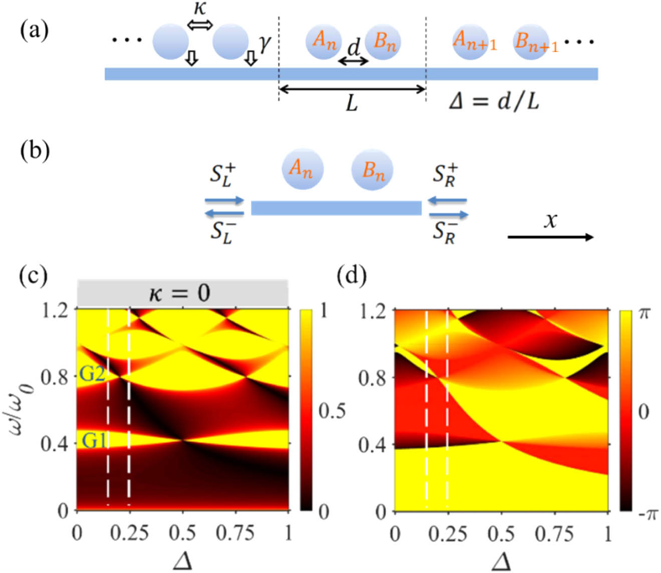
Figure 1.(a) 1D dimerized chain with the unit cell length
The transfer matrix of a unit cell in the EM system can be obtained from Eq. (3) by rearranging the incidence waves and outgoing waves as
We suppose
Then, we can calculate the band structures, as well as the transmission and reflection coefficients for the 1D chains based on the scattering matrix.
The topological phase transitions are commonly accompanied by the closing and reopening of the band gaps, which correspond to the total reflection bands for a semi-infinite structure. We first calculate the reflectivity and reflection phase of a semi-infinite dimerized chain with the help of impedance boundary condition (see Appendix A), with the fitted parameters
3. TOPOLOGICAL PHASE TRANSITION IN THE 1D DIMERIZED HYBRID-COUPLING PTIs
Next, we extend the multiple scattering theory into the 1D dimerized far-field coupling model with additional near-field coupling between two scatters
![]()
Figure 2.(a) Reflectivity and (b) reflection phase of the semi-infinite 1D dimerized chain with intracell near-field coupling
To investigate in detail the modulation of topological properties in the presence of near-field coupling, the reflectivity and reflection phase are given in Fig. 3 as functions of near-field coupling
![]()
Figure 3.(a) Reflectivity and (b) reflection phase of the semi-infinite 1D dimerized chain as functions of near-field coupling and frequency for a specific dimerized parameter
To fully uncover the topological properties of this hybrid coupling 1D model, we give the band structures of hybrid systems. In the condition of the Bloch boundary condition
The dispersion relation cannot be presented as an elegant analytical solution because of the complexity of this model. But we can numerically calculate the band structures for different near-field coupling strengths
![]()
Figure 4.Band structures of infinite 1D dimerized chain for a fixed dimerized parameter
We calculate the Zak phases of the first few bands to describe the topological transition quantitatively. Zak phases are initially defined as the characteristic quantity to describe the electron movement in a 1D periodic solid system [54] and then extended to a 1D photonic system with mirror symmetry to depict the topological properties of pass bands. Generally, the Zak phase can be calculated based on the original definition. First, one can find the period part
The Zak phase of an isolated band can also be determined by identifying all zero-reflection states of the semi-infinite 1D chain (or a single unit cell). It has been demonstrated that each zero-reflection state corresponding to a singular point of zero reflection in reflection spectrum contributes
The band inversion leads to contributing
It should be mentioned that all band gaps are direct band gaps for the previously studied 1D dimerized chains with either far-field or near-field coupling only. Figure 4(a) shows an example of far-field coupling PTIs, where the momenta of the bottom of the upper band and the top of the lower band are always the same [47]. This situation has changed with the introduction of hybrid coupling. It has been shown in Figs. 4(b)–4(f) that an indirect band gap appears in the band diagram for the hybrid-coupling PTIs. For example, the gap G3 becomes an indirect gap when the near-field coupling is small (
For a clearer insight into the effects of joint modulation of near-field and far-field couplings on the topological properties, the Zak phase diagram of the second pass band in the parameters space composed of
![]()
Figure 5.Zak phase diagram of the second band under the joint modulation of near-field coupling
4. EXPERIMENTAL DEMONSTRATION OF TOPOLOGICAL INTERFACE STATE WITH HYBRID COUPLING PTIs
Microwave experiments based on microstrip transmission line are conducted to demonstrate the hybrid-coupling-induced topological transition by measuring the reflection or transmission coefficients of the samples. The topologically distinguished two chains are composed of five unit cells with
![]()
Figure 6.(a) Three samples of 1D chain for (I) dimerized parameter
We can theoretically calculate the reflection coefficient of the EM wave incident to the quasi-1D chain to compare it with the experimental results. The transfer matrix of a unit cell in the EM system is noted in Eq. (4). For five unit cells, the total transfer matrix
The experimental and theoretical results of the reflection coefficients are shown in Fig. 6. The reflection spectra for sample I and sample II in Fig. 6(a) are plotted in Figs. 6(b) and 6(c), respectively. Three band gaps with high reflectivity represented by the gray area are shown in Figs. 6(b) and 6(c). The calculation results (black lines) of reflection amplitude agree well with the measurements (red dots). For the 2nd band gaps (G2), the reflection phases of the two samples are with opposite signs. The different sign of reflection phases for the 2nd band gaps indicates the topological transition induced by hybrid coupling in this 1D structure.
To further verify the different topological properties of these two dimerized chains, the topological interface state in sample III [see Fig. 6(a)] is investigated. The sample III is composed by two paired chains with a total length of 240 mm. According to surface bulk correspondence, there will be an interface mode emerging in the original gap G2 because of the opposite signs of the reflection phase. As shown in Fig. 6(d), a reflection valley indeed appears in the gap G2 region for the sample III in both calculated and measured reflection spectra. Moreover, the measured and simulated (CST MICROWAVE STUDIO) electric field distribution (in the backbone waveguide) at this reflection valley frequency (
5. CONCLUSION
In summary, we theoretically and experimentally investigate the topological properties of a dimerized 1D chain modulated by hybrid coupling. The introduced intracell near-field coupling in a far-field coupling dimerized chain can induce band inversion without tuning the dimerized parameter. Zak phases in this hybrid coupling model for different near-field couplings are investigated in detail. The interface mode is realized by pairing two dimerized chains with opposite reflection phases in the second band gaps to further confirm the topological phase transition. In addition, we notice that there are indirect band gaps in the hybrid coupling PTIs, and the near-field coupling only modulates the dispersion of the bands around the scatter resonance frequency. A flat band can be achieved by properly choosing the coupling parameters. The unit, which is near-field and far-field coupled to the other unit, is an analogue to the giant atom with multiple coupling channels in a quantum-waveguide system [61–63]. Hence, our model may provide a potential platform to study the interplay between giant atoms and topology. The results in our paper can be extended to a 2D case and even higher dimension.
APPENDIX A: CALCULATION OF THE REFLECTION COEFFICIENT FOR THE SEMI-INFINITE 1D CHAIN
In this appendix, the calculation of the reflection coefficient for the semi-infinite dimerized 1D chain is shown. The transfer matrix related to the incoming wave and outcoming wave for the
From Eqs. (
As our system is passive, the real part of impedance
APPENDIX B: DETERMINATION OF EFFECTIVE PERMITTIVITY AND PERMEABILITY OF THE 1D PHOTONICS METAMATERIALS
In this appendix, we show that the effective relative permittivity (
For a 1D metamaterial with length
Here,
For the passive materials, the requirement that
APPENDIX C: DETERMINATION OF THE PARAMETERS THROUGH CURVE FITTINGS
In this appendix, the fitted parameters of far-field coupling
First, we show how to obtain the values of far-field coupling
![]()
Figure 7.(a) Schematic of a side resonant branch excited by the EM waves from Port1 and (b) the simulation (black line) and fitted reflectivity (red line) of the EM wave. (c) Near-field coupling and far-field coupling coexist between two resonant branches in the same unit cell and (d) the simulation (black line) and fitted reflectivity (red line) when the EM wave is incident from the left.
By fitting the reflectivity obtained from the simulation with Eq. (
Next the same method is used to find out the value of near-field coupling
References
[1] C. L. Kane, E. J. Mele. Quantum spin Hall effect in graphene. Phys. Rev. Lett., 95, 226801(2005).
[2] N. H. Lindner, G. Refael, V. Galitski. Floquet topological insulator in semiconductor quantum wells. Nat. Phys., 7, 490-495(2011).
[3] D. J. Thouless, M. Kohmoto, M. P. Nightingale, M. den Nijs. Quantized Hall conductance in a two-dimensional periodic potential. Phys. Rev. Lett., 49, 405-408(1982).
[4] X. G. Wen. Topological orders and edge excitations in fractional quantum Hall states. Adv. Phys., 44, 405-473(1995).
[5] Z. Wang, Y. D. Chong, J. D. Joannopoulos, M. Soljačić. Reflection-free one-way edge modes in a gyromagnetic photonic crystal. Phys. Rev. Lett., 100, 013905(2008).
[6] H. Zhao, X. Qiao, T. Wu, B. Midya, S. Longhi, L. Feng. Non-Hermitian topological light steering. Science, 365, 1163-1166(2019).
[7] C. Lu, C. Wang, M. Xiao, Z. Q. Zhang, C. T. Chan. Topological rainbow concentrator based on synthetic dimension. Phys. Rev. Lett., 126, 113902(2021).
[8] H. Zhang, L. Qian, C. Wang, C.-Y. Ji, Y. Liu, J. Chen, C. Lu. Topological rainbow based on graded topological photonic crystals. Opt. Lett., 46, 1237-1240(2021).
[9] M. Atala, M. Aidelsburger, J. T. Barreiro, D. Abanin, T. Kitagawa, E. Demler, I. Bloch. Direct measurement of the Zak phase in topological Bloch bands. Nat. Phys., 9, 795-800(2013).
[10] F. Gao, Z. Gao, X. Shi, Z. Yang, X. Lin, H. Xu, J. D. Joannopoulos, M. Soljačić, H. Chen, L. Lu, Y. Chong, B. Zhang. Probing topological protection using a designer surface plasmon structure. Nat. Commun., 7, 11619(2016).
[11] Z. Gao, Z. Yang, F. Gao, H. Xue, Y. Yang, J. Dong, B. Zhang. Valley surface-wave photonic crystal and its bulk/edge transport. Phys. Rev. B, 96, 201402(2017).
[12] A. B. Khanikaev, S. H. Mousavi, W.-K. Tse, M. Kargarian, A. H. MacDonald, G. Shvets. Photonic topological insulators. Nat. Mater., 12, 233-239(2013).
[13] M. Kremer, I. Petrides, E. Meyer, M. Heinrich, O. Zilberberg, A. Szameit. A square-root topological insulator with non-quantized indices realized with photonic Aharonov-Bohm cages. Nat. Commun., 11, 907(2020).
[14] J. Ma, J.-W. Rhim, L. Tang, S. Xia, H. Wang, X. Zheng, S. Xia, D. Song, Y. Hu, Y. Li, B.-J. Yang, D. Leykam, Z. Chen. Direct observation of flatband loop states arising from nontrivial real-space topology. Phys. Rev. Lett., 124, 183901(2020).
[15] M. C. Rechtsman, Y. Plotnik, J. M. Zeuner, D. Song, Z. Chen, A. Szameit, M. Segev. Topological creation and destruction of edge states in photonic graphene. Phys. Rev. Lett., 111, 103901(2013).
[16] J. Song, F. Yang, Z. Guo, X. Wu, K. Zhu, J. Jiang, Y. Sun, Y. Li, H. Jiang, H. Chen. Wireless power transfer via topological modes in dimer chains. Phys. Rev. Appl., 15, 014009(2021).
[17] S. Xia, D. Song, N. Wang, X. Liu, J. Ma, L. Tang, H. Buljan, Z. Chen. Topological phenomena demonstrated in photorefractive photonic lattices. Opt. Mater. Express, 11, 1292-1312(2021).
[18] M. Xiao, Z. Q. Zhang, C. T. Chan. Surface impedance and bulk band geometric phases in one-dimensional systems. Phys. Rev. X, 4, 021017(2014).
[19] M. Li, D. Zhirihin, M. Gorlach, X. Ni, D. Filonov, A. Slobozhanyuk, A. Alù, A. B. Khanikaev. Higher-order topological states in photonic Kagome crystals with long-range interactions. Nat. Photonics, 14, 89-94(2020).
[20] S. Liu, S. Ma, Q. Zhang, L. Zhang, C. Yang, O. You, W. Gao, Y. Xiang, T. J. Cui, S. Zhang. Octupole corner state in a three-dimensional topological circuit. Light Sci. Appl., 9, 145(2020).
[21] B.-Y. Xie, G.-X. Su, H.-F. Wang, H. Su, X.-P. Shen, P. Zhan, M.-H. Lu, Z.-L. Wang, Y.-F. Chen. Visualization of higher-order topological insulating phases in two-dimensional dielectric photonic crystals. Phys. Rev. Lett., 122, 233903(2019).
[22] Y. Yang, Z. Gao, H. Xue, L. Zhang, M. He, Z. Yang, R. Singh, Y. Chong, B. Zhang, H. Chen. Realization of a three-dimensional photonic topological insulator. Nature, 565, 622-626(2019).
[23] S. Weimann, M. Kremer, Y. Plotnik, Y. Lumer, S. Nolte, K. G. Makris, M. Segev, M. C. Rechtsman, A. J. N. Szameit. Topologically protected bound states in photonic parity–time-symmetric crystals. Nat. Mater., 16, 433-438(2017).
[24] D.-W. Zhang, L.-Z. Tang, L.-J. Lang, H. Yan, S.-L. Zhu. Non-Hermitian topological Anderson insulators. Sci. China: Phys., Mech. Astron., 63, 267062(2020).
[25] M. Guo, S. Xia, N. Wang, D. Song, Z. Chen, J. Yang. Weakly nonlinear topological gap solitons in Su–Schrieffer–Heeger photonic lattices. Opt. Lett., 45, 6466-6469(2020).
[26] M. C. Rechtsman, J. M. Zeuner, Y. Plotnik, Y. Lumer, D. Podolsky, F. Dreisow, S. Nolte, M. Segev, A. J. N. Szameit. Photonic Floquet topological insulators. Nature, 496, 196-200(2013).
[27] F. D. M. Haldane, S. Raghu. Possible realization of directional optical waveguides in photonic crystals with broken time-reversal symmetry. Phys. Rev. Lett., 100, 013904(2008).
[28] Z. Wang, Y. Chong, J. D. Joannopoulos, M. Soljačić. Observation of unidirectional backscattering-immune topological electromagnetic states. Nature, 461, 772-775(2009).
[29] M. Hafezi, E. A. Demler, M. D. Lukin, J. M. Taylor. Robust optical delay lines with topological protection. Nat. Phys., 7, 907-912(2011).
[30] K. Lai, T. Ma, X. Bo, S. Anlage, G. Shvets. Experimental realization of a reflections-free compact delay line based on a photonic topological insulator. Sci. Rep., 6, 28453(2016).
[31] S. A. Mann, D. L. Sounas, A. Alù. Broadband delay lines and nonreciprocal resonances in unidirectional waveguides. Phys. Rev. B, 100, 020303(2019).
[32] K. Fang, J. Luo, A. Metelmann, M. H. Matheny, F. Marquardt, A. A. Clerk, O. Painter. Generalized non-reciprocity in an optomechanical circuit via synthetic magnetism and reservoir engineering. Nat. Phys., 13, 465-471(2017).
[33] W. Gao, X. Hu, C. Li, J. Yang, Z. Chai, J. Xie, Q. Gong. Fano-resonance in one-dimensional topological photonic crystal heterostructure. Opt. Express, 26, 8634-8644(2018).
[34] X. Wang, Y. Liang, L. Wu, J. Guo, X. Dai, Y. Xiang. Multi-channel perfect absorber based on a one-dimensional topological photonic crystal heterostructure with graphene. Opt. Lett., 43, 4256-4259(2018).
[35] S. Longhi. Zak phase of photons in optical waveguide lattices. Opt. Lett., 38, 3716-3719(2013).
[36] J. Lu, L. He, Z. Addison, E. J. Mele, B. Zhen. Floquet topological phases in one-dimensional nonlinear photonic crystals. Phys. Rev. Lett., 126, 113901(2021).
[37] A. Poddubny, A. Miroshnichenko, A. Slobozhanyuk, Y. Kivshar. Topological Majorana states in zigzag chains of plasmonic nanoparticles. ACS Photon., 1, 101-105(2014).
[38] C. Schmidt, A. Palatnik, M. Sudzius, S. Meister, K. Leo. Coupled topological interface states. Phys. Rev. B, 103, 085412(2021).
[39] A. P. Slobozhanyuk, A. N. Poddubny, A. E. Miroshnichenko, P. A. Belov, Y. S. Kivshar. Subwavelength topological edge states in optically resonant dielectric structures. Phys. Rev. Lett., 114, 123901(2015).
[40] Q. Wang, M. Xiao, H. Liu, S. Zhu, C. T. Chan. Measurement of the Zak phase of photonic bands through the interface states of a metasurface/photonic crystal. Phys. Rev. B, 93, 041415(2016).
[41] N. Malkova, I. Hromada, X. Wang, G. Bryant, Z. Chen. Observation of optical Shockley-like surface states in photonic superlattices. Opt. Lett., 34, 1633-1635(2009).
[42] N. Malkova, I. Hromada, X. Wang, G. Bryant, Z. Chen. Transition between Tamm-like and Shockley-like surface states in optically induced photonic superlattices. Phys. Rev. A, 80, 043806(2009).
[43] M. Di Liberto, A. Recati, I. Carusotto, C. Menotti. Two-body physics in the Su–Schrieffer–Heeger model. Phys. Rev. A, 94, 062704(2016).
[44] G. Go, I.-S. Hong, S.-W. Lee, S. K. Kim, K.-J. Lee. Realization of Su-Schrieffer-Heeger states based on metamaterials of magnetic solitons. Phys. Rev. B, 101, 134423(2020).
[45] L.-J. Lang, Y. Wang, H. Wang, Y. D. Chong. Effects of non-Hermiticity on Su–Schrieffer–Heeger defect states. Phys. Rev. B, 98, 094307(2018).
[46] N. Kaina, R. Fleury. Hermitian formulation of multiple scattering induced topological phases in metamaterial crystals. Phys. Rev. B, 102, 134303(2020).
[47] W. Zhu, Y.-Q. Ding, J. Ren, Y. Sun, Y. Li, H. Jiang, H. Chen. Zak phase and band inversion in dimerized one-dimensional locally resonant metamaterials. Phys. Rev. B, 97, 195307(2018).
[48] C. W. Hsu, B. Zhen, A. D. Stone, J. D. Joannopoulos, M. Soljačić. Bound states in the continuum. Nat. Rev. Mater., 1, 16048(2016).
[49] J. W. Rao, Y. T. Zhao, Y. S. Gui, X. L. Fan, D. S. Xue, C. M. Hu. Controlling microwaves in non-Hermitian metamaterials. Phys. Rev. Appl., 15, L021003(2021).
[50] E. Lamothe, G. Leveque, O. J. F. Martin. Optical forces in coupled plasmonic nanosystems: near field and far field interaction regimes. Opt. Express, 15, 9631-9644(2007).
[51] B. Gallinet, O. J. F. Martin. Relation between near-field and far-field properties of plasmonic Fano resonances. Opt. Express, 19, 22167-22175(2011).
[52] S. H. Fan, W. Suh, J. D. Joannopoulos. Temporal coupled-mode theory for the Fano resonance in optical resonators. J. Opt. Soc. Am. A, 20, 569-572(2003).
[53] W. Tan, Y. Sun, Z.-G. Wang, H. Chen. Manipulating electromagnetic responses of metal wires at the deep subwavelength scale via both near- and far-field couplings. Appl. Phys. Lett., 104, 091107(2014).
[54] J. Zak. Berry’s phase for energy-bands in solids. Phys. Rev. Lett., 62, 2747-2750(1989).
[55] J. Guo, Y. Sun, Y. Zhang, H. Li, H. Jiang, H. Chen. Experimental investigation of interface states in photonic crystal heterostructures. Phys. Rev. E, 78, 026607(2008).
[56] Q. Huang, Z. Guo, J. Feng, C. Yu, H. Jiang, Z. Zhang, Z. Wang, H. Chen. Observation of a topological edge state in the X-ray band. Laser Photon. Rev., 13, 1800339(2019).
[57] X. Shi, C. Xue, H. Jiang, H. Chen. Topological description for gaps of one-dimensional symmetric all-dielectric photonic crystals. Opt. Express, 24, 18580-18591(2016).
[58] W. Tan, Y. Sun, H. Chen, S.-Q. Shen. Photonic simulation of topological excitations in metamaterials. Sci. Rep., 4, 3842(2014).
[59] D. R. Smith, S. Schultz, P. Markos, C. M. Soukoulis. Determination of effective permittivity and permeability of metamaterials from reflection and transmission coefficients. Phys. Rev. B, 65, 195104(2002).
[60] C. F. Coombs. Printed Circuits Handbook(2008).
[61] L. Guo, A. F. Kockum, F. Marquardt, G. Johansson. Oscillating bound states for a giant atom. Phys. Rev. Res., 2, 043014(2020).
[62] M. V. Gustafsson, T. Aref, A. F. Kockum, M. K. Ekstrom, G. Johansson, P. Delsing. Propagating phonons coupled to an artificial atom. Science, 346, 207-211(2014).
[63] A. M. Vadiraj, A. Ask, T. G. McConkey, I. Nsanzineza, C. W. S. Chang, A. F. Kockum, C. M. Wilson. Engineering the level structure of a giant artificial atom in waveguide quantum electrodynamics. Phys. Rev. A, 103, 023710(2021).


Set citation alerts for the article
Please enter your email address

© Copyright 2018-2021 | Chinese Laser Press. All Rights Reserved 沪ICP备15018463号-20