
Woo-Bin Lee, Chul-Soon Im, Changyi Zhou, Bishal Bhandari, Duk-Yong Choi, Sang-Shin Lee, "Metasurface doublet-integrated bidirectional grating antenna enabling enhanced wavelength-tuned beam steering," Photonics Res. 10, 248 (2022)
- Photonics Research
- Vol. 10, Issue 1, 248 (2022)
Abstract
1. INTRODUCTION
Optical phased array (OPA) is widely perceived as an outstanding beam-steering strategy owing to its salient advantages that include a low divergent beam, flexible 2D beamforming, and ultrafast inertia-free steering [1–6]. Integrated-circuit type OPAs, which are a prominent candidate for light detection and ranging (lidar), have attracted immense interest for applications such as sensing, 3D mapping, navigation for self-driving cars, and autonomous drones [7–11]. However, solid-state beam steering suffers from a narrower field of view than mechanical methods such as a micro–electromechanical system (MEMS) mirror, gimbal, and prism [12–14]. The scanning span along the longitudinal direction of an OPA is determined by the wavelength tuning range of the light source as well as the diffraction grating constituting the OPA. A waveguide diffraction grating delivers a typically small angular dispersion of below 0.140 deg/nm [15]. Thus, a broadband tunable laser with a tuning range exceeding 100 nm was used to expand the steering range [1,15–19]. However, a widely tunable laser is extremely difficult to embody and requires complex control schemes to access all wavelengths [20,21]. The beam-steering range in the longitudinal direction should be addressed to overcome the inherent limitations of OPA-based emitters.
Recently, various configurations of lenses and prisms, which are used to manipulate a beam in free space, have been devised to execute wide-angle beam steering by amplifying the steering efficiency [15,22–24]. These methods are known for demonstrating wide-angle steering, but require bulky components and mounting fixtures with dimensions of several centimeters. Compared to the bulky lens systems, a metasurface device, featuring an ultrathin, flat form factor, can be engineered to provide high design flexibility [25–28]. Studies have attempted to directly integrate such metasurfaces into a silicon photonic circuit to contrive compact beam manipulations in terms of emission positions and radiation modes [25,29]. Nonetheless, a common monolayer metasurface may be limited in increasing the field of view of an OPA [25,30,31]. In this context, the steering efficiency (deg/nm) of the OPA, determined by an angular shift in response to a wavelength tuning, can be enhanced significantly by relying on a metasurface doublet (MD), as reported in our previous work [31]. To date, to the best of our knowledge, no studies have reported research on an MD in conjunction with a silicon photonic bidirectional grating antenna (BDGA) to efficiently enhance the beam steering efficiency.
This work presents a BDGA that incorporates an MD featuring a flat and ultrathin form factor for efficient beam steering. Compared to conventional grating antennas, the BDGA, which is capable of bidirectional beam steering, effectively imparts twice the steering range within a given wavelength-tuning range. The steering performance of the BDGA, which emits light in a vertical direction, is characterized in terms of the steering range and spectral emission response of the main beam along the longitudinal direction. Furthermore, the MD, operating as a steering angle magnifying metalens is integrated into the BDGA to amplify threefold the wavelength-tuned steering efficiency. The ultrathin and polarization-insensitive MD that constitutes two disparate metasurfaces enables relatively straightforward alignment with the silicon photonic circuit for performance improvement. Finally, the emission response of the MD-integrated BDGA is analyzed after evaluating the transfer characteristic of the MD. We believe this approach provides a functional flat form factor to realize an OPA with high beam-steering efficiency.
2. DESIGN OF THE PROPOSED BDGA AND MD TO BOOST THE BEAM-STEERING EFFICIENCY
The narrow beam-steering range in a nonmechanical system can be dramatically extended by resorting to lens optics [22,23]. This approach can be similarly applied to enhance the steering performance of an OPA to substantially expand the achievable scanning range under a given wavelength-tuning range. Figure 1 depicts the schematic configuration of the proposed scheme, in which an MD is incorporated atop a BDGA to further enhance the beam steering. The BDGA chip in silicon is configured so that light is launched through a spot size converter and split into five stages of
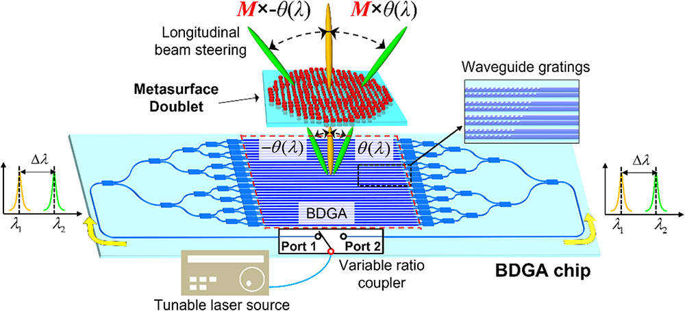
Figure 1.Schematic configuration of the proposed BDGA incorporating an MD, enabling an enhanced beam-steering efficiency in the longitudinal direction.
A. Proposed BDGA Enabling Bidirectional Beam Emission
Figure 2(a) illustrates a schematic of the suggested BDGA and its principle of operation. Silicon nitride (SiN) is used for the waveguide core because of its advantages of a broad transparency window, low loss, and conspicuous fabrication reliability [32–34]. A SiN waveguide with a thickness (
![]()
Figure 2.(a) Configuration of the proposed BDGA and its operation that extends the beam-steering range. (b) Calculated spectral emission response with respect to the grating period for a 2D modeled BDGA for
Unlike conventional grating counterparts, the proposed BDGA can support bidirectional beam radiation by alternately feeding light to the two ports. The emission angle
For a 2D modeled SiN antenna, as illustrated in Fig. 2(b), the emission spectra are numerically designed to radiate the beam normally with the assistance of Lumerical FDTD Solutions (Ansys Lumerical). A 500 μm long SiN waveguide incorporates a partially etched surface grating, with a fill factor of 0.5 and a height of 90 nm. The effective refractive index of the waveguide was calculated as
B. MD as a Steering Angle Magnifying Metalens
Figure 3(a) describes the concept of an ultrathin lens system that taps into the MD to increase the steering efficiency. Here, the MD comprises a glass substrate with a thickness of 902 μm, sandwiched between metasurface 1 (MS1) and metasurface 2 (MS2), which function as convex and concave lenses, respectively. MS1 and MS2 comprise circular nanopillars in hydrogenated amorphous silicon (a-Si:H), with heights of 880 nm. The simulated magnetic field is displayed for a-Si:H nanopillars, showing that the field is strongly confined inside the nanopillar. By regulating the diameters of the pillars from 200 to 494 nm, the incident light was manipulated to sufficiently undergo a phase shift covering a span of 0 to
![]()
Figure 3.(a) Configuration of the proposed MD, comprising MS1 and MS2, facilitating the magnification of the beam-steering range. A meta-atom (or unit cell) and the highly confined magnetic field are also included. (b) Designed phase profile of the MD and (c) SEM images of the fabricated MS1 and MS2.
3. RESULTS AND DISCUSSIONS
A. Characterization of the Fabricated BDGA
Figure 4(a) presents the test setup to evaluate the beam-steering efficiency of the proposed BDGA. A tunable laser (Santec Corp., TLS-210) serves as a light source to provide a wide range of wavelengths between 1530 and 1600 nm. Light was directed to a variable ratio coupler (KS Photonics Inc.) through an erbium-doped fiber amplifier. To fulfill selective optical feeding to the two ports of the BDGA, we used a coupler instead of a
![]()
Figure 4.(a) Experimental setup to inspect the performance of the prepared BDGA. (b) Captured intensity profiles of the wavelength-tuned main beam. (c) Observed emission angles corresponding to the main beam in terms of the wavelength.
Figure 5 shows the beam emission efficiency corresponding to the main beam for a wavelength of 1530–1600 nm. The efficiency declined slightly with increasing wavelengths owing to the presence of a resonance dip, which was forged at longer wavelengths [36], resulting in a variation of
![]()
Figure 5.Measured emission efficiency of the main beam versus the wavelength.
B. Deflection and Transmission Characteristics of the MD
We experimentally investigated the optical response of the MD before its incorporation into the BDGA, as delineated in Fig. 6(a). A collimated beam is polarized and directed toward the MD via a pinhole, with a diameter of 300 μm, to constrict the beam size. The deflected beam emerging from the MD was monitored using a beam profiler. Figure 6(b) shows the angle (
![]()
Figure 6.(a) Test setup to examine the beam deflection based on the MD with the incident angle. (b) Measured deflection angle and deflection efficiency. (c) Relative deflected beam power as a function of the incident angle.
C. Evaluation of the BDGA Incorporating the MD
Figure 7(a) shows microscopic images of the top and side views of the BDGA combined with the MD. The substrate of the MD is placed squarely above the BDGA chip, which is fixed by a holder. The gap between the BDGA and MD is meticulously adjusted to be below 1 mm through an XYZ translation stage. The tilt error of the MD, which may distort the beam profile and induce an angular offset, has been effectively prevented. Light is alternately launched toward Ports 1 and 2 of the BDGA, and the beam emanating from the BDGA is deliberately deflected by the MD mounted atop it. Figure 7(b) illustrates the observed main beam profiles of the BDGA and the BDGA integrated with the MD, as projected on a beam profiler at the same distance. The MD is deemed to expand the size of the main beam, whose divergence is tripled to assume 1.8° and 0.7° along the transverse and longitudinal directions, respectively. The beam divergence was correspondingly enlarged three times omnidirectionally, which might possibly deteriorate the angular resolution. This problem may be mitigated by increasing the number of grating antenna elements to enlarge the aperture [2]. The transfer characteristics of the MD-integrated BDGA were scrutinized in terms of the steering angle in the wavelength range of 1530 and 1595 nm, as shown in Fig. 7(c). When the angular range of the beam impinging upon the MD was
![]()
Figure 7.(a) Side and top views of the BDGA integrated with the MD. (b) Captured intensity profiles of the main beam radiated from BDGA without and with the MD. (c) Measured beam emission angle versus the wavelength. (d) Measured total efficiency of the main beam deflected by the MD versus the wavelength.
We have explored the optical throughput of the main beam, emerging from the MD, by monitoring the corresponding power captured by the receiving photodiode (Thorlabs, S132C), inclusive of the coupling associated with the spot size converter, as shown in Fig. 7(d). The total efficiency was observed to vary between
4. CONCLUSION
We demonstrated highly efficient beam steering with a BDGA incorporating an MD. The steering efficiency of the proposed BDGA was obtained as approximately 0.148 deg/nm, which was doubled by bidirectionally feeding the light. The structure of the BDGA provided stability to the emission spectral response and enabled vertical radiation, ensuring its suitability for magnifying steering angle devices. An ultrathin, polarization-insensitive MD amplifying the angle of beam steering was used to enhance the steering efficiency of the nonmechanical beam scanner. The implemented MD, which increased the steering efficiency threefold, was mounted on top of the BDGA, thereby expanding its steering range. We verified that our platform improves the steering performance, and had a compact form factor compared to that of conventional bulky lens systems. Finally, the wavelength-tuned steering efficiency was 0.461 deg/nm, which represents a threefold increase over a conventional grating antenna within a given wavelength-tuning range. The proposed approach, which greatly enhances beam-steering efficiency while minimizing space consumption, could facilitate the development of practical solid-state beam steering.
Acknowledgment
Acknowledgment. The authors are grateful to Ligentec for device fabrication. This work has been made possible through access to the ACT node of the Australian National Fabrication Facility (ANFF).
References
[1] D. N. Hutchison, J. Sun, J. K. Doylend, R. Kumar, J. Heck, W. Kim, C. T. Phare, A. Feshali, H. Rong. High-resolution aliasing-free optical beam steering. Optica, 3, 887-890(2016).
[2] M. R. Kossey, C. Rizk, A. C. Foster. End-fire silicon optical phased array with half-wavelength spacing. APL Photon., 3, 011301(2018).
[3] W. Xu, L. Zhou, L. Lu, J. Chen. Aliasing-free optical phased array beam-steering with a plateau envelope. Opt. Express, 27, 3354-3368(2019).
[4] J. Sun, E. Timurdogan, A. Yaacobi, E. S. Hosseini, M. R. Watts. Large-scale nanophotonic phased array. Nature, 493, 195-199(2013).
[5] W. Guo, P. R. A. Binetti, C. Althouse, M. L. Mašanović, H. P. M. M. Ambrosius, L. A. Johansson, L. A. Coldren. Two-dimensional optical beam steering with InP-based photonic integrated circuits. IEEE J. Sel. Top. Quantum Electron., 19, 6100212(2013).
[6] J. C. Hulme, J. K. Doylend, M. J. R. Heck, J. D. Peters, M. L. Davenport, J. T. Bovington, L. A. Coldren, J. E. Bowers. Fully integrated hybrid silicon two dimensional beam scanner. Opt. Express, 23, 5861-5874(2015).
[7] C.-P. Hsu, B. Li, B. Solano-Rivas, A. R. Gohil, P. H. Chan, A. D. Moore, V. Donzella. A review of and perspective on optical phased array for automotive LiDAR. IEEE J. Sel. Top. Quantum Electron., 27, 8300416(2021).
[8] S. A. Miller, C. T. Phare, Y.-C. Chang, X. Ji, O. A. J. Gordillo, A. Mohanty, S. P. Roberts, M. C. Shin, B. Stern, M. Zadka, M. Lipson. 512-element actively steered silicon phased array for low-power LIDAR. Conference on Lasers and Electro-Optics (CLEO), JTh5C.2(2018).
[9] C. V. Poulton. Integrated LIDAR with optical phased arrays in silicon photonics(2016).
[10] S. Chung, H. Abediasl, H. Hashemi. A monolithically integrated large-scale optical phased array in silicon-on-insulator CMOS. IEEE J. Solid-State Circuits, 53, 275-296(2018).
[11] F. Aflatouni, B. Abiri, A. Rekhi, A. Hajimiri. Nanophotonic projection system. Opt. Express, 23, 21012-21022(2015).
[12] M. Zadka, Y.-C. Chang, A. Mohanty, C. T. Phare, S. P. Roberts, M. Lipson. On-chip platform for a phased array with minimal beam divergence and wide field-of-view. Opt. Express, 26, 2528-2534(2018).
[13] P. F. Van Kessel, L. J. Hornbeck, R. E. Meier, M. R. Douglass. A MEMS-based projection display. Proc. IEEE, 86, 1687-1704(1998).
[14] W. S. Rabinovich, C. I. Moore, R. Mahon, P. G. Goetz, H. R. Burris, M. S. Ferraro, J. L. Murphy, L. M. Thomas, G. C. Gilbreath, M. Vilcheck, M. R. Suite. Free-space optical communications research and demonstrations at the U.S. Naval Research Laboratory. Appl. Opt., 54, F189-F200(2015).
[15] H. Ito, Y. Kusunoki, J. Maeda, D. Akiyama, N. Kodama, H. Abe, R. Tetsuya, T. Baba. Wide beam steering by slow-light waveguide gratings and a prism lens. Optica, 7, 47-52(2020).
[16] J. K. Doylend, M. J. R. Heck, J. T. Bovington, J. D. Peters, L. A. Coldren, J. E. Bowers. Two-dimensional free-space beam steering with an optical phased array on silicon-on-insulator. Opt. Express, 19, 21595-21604(2011).
[17] D. Kwong, A. Hosseini, J. Covey, Y. Zhang, X. Xu, H. Subbaraman, R. T. Chen. On-chip silicon optical phased array for two-dimensional beam steering. Opt. Lett., 39, 941-944(2014).
[18] K. V. Acoleyen, W. Bogaerts, J. Jágerská, N. Le Thomas, R. Houdré, R. Baets. Off-chip beam steering with a one-dimensional optical phased array on silicon-on-insulator. Opt. Lett., 34, 1477-1479(2009).
[19] Y. Zhu, S. Zeng, L. Zhu. Optical beam steering by using tunable, narrow-linewidth butt-coupled hybrid lasers in a silicon nitride photonics platform. Photon. Res., 8, 375-380(2020).
[20] S. Matsuo, T. Segawa. Microring-resonator-based widely tunable lasers. IEEE J. Sel. Top. Quantum Electron., 15, 545-553(2009).
[21] G.-L. Su, M. C. Wu. Widely tunable semiconductor lasers with three interferometric arms. Opt. Express, 25, 21400-21409(2017).
[22] M. Zohrabi, R. H. Cormack, J. T. Gopinath. Wide-angle nonmechanical beam steering using liquid lenses. Opt. Express, 24, 23798-23809(2016).
[23] M. Zohrabi, W. Y. Lim, R. H. Cormack, O. D. Supekar, V. M. Bright, J. T. Gopinath. Lidar system with nonmechanical electrowetting-based wide-angle beam steering. Opt. Express, 27, 4404-4415(2019).
[24] C.-S. Im, S.-M. Kim, K.-P. Lee, S.-H. Ju, J.-H. Hong, S.-W. Yoon, T. Kim, E.-S. Lee, B. Bhandari, C. Zhou, S.-Y. Ko, Y.-H. Kim, M.-C. Oh, S.-S. Lee. Hybrid integrated silicon nitride–polymer optical phased array enabling efficient light detection and ranging. J. Lightwave Technol., 39, 4402-4409(2021).
[25] Y.-C. Chang, M. C. Shin, C. T. Phare, S. A. Miller, E. Shim, M. Lipson. 2D beam steerer based on metalens on silicon photonics. Opt. Express, 29, 854-864(2021).
[26] L. Jin, Z. Dong, S. Mei, Y. F. Yu, Z. Wei, Z. Pan, S. D. Rezaei, X. Li, A. I. Kuznetsov, Y. S. Kivshar, J. K. W. Yang, C.-W. Qiu. Noninterleaved metasurface for (26−1) spin- and wavelength-encoded holograms. Nano Lett., 18, 8016-8024(2018).
[27] M. Khorasaninejad, W. T. Chen, R. C. Devlin, J. Oh, A. Y. Zhu, F. Capasso. Metalenses at visible wavelengths: diffraction-limited focusing and subwavelength resolution imaging. Science, 352, 1190-1194(2016).
[28] L. Jin, Y.-W. Huang, Z. Jin, R. C. Devlin, Z. Dong, S. Mei, M. Jiang, W. T. Cheng, Z. Wei, H. Liu, J. Teng, A. Danner, X. Li, S. Xiao, S. Zhang, C. Yu, J. K. W. Yang, F. Capasso, C.-W. Qiu. Dielectric multi-momentum meta-transfer in the visible. Nat. Commun., 10, 4789(2019).
[29] A. Yulaev, W. Zhu, C. Zhang, D. A. Westly, H. J. Lezec, A. Agrawal, V. Aksyuk. Metasurface-integrated photonic platform for versatile free-space beam projection with polarization control. ACS Photon., 6, 2902-2909(2019).
[30] A. Arbabi, E. Arbabi, S. M. Kamali, Y. Horie, S. Han, A. Faraon. Miniature optical planar camera based on a wide-angle metasurface doublet corrected for monochromatic aberrations. Nat. Commun., 7, 13682(2016).
[31] C. Zhou, W.-B. Lee, C.-S. Park, S. Gao, D.-Y. Choi, S.-S. Lee. Multifunctional beam manipulation at telecommunication wavelengths enabled by an all-dielectric metasurface doublet. Adv. Opt. Mater., 8, 2000645(2020).
[32] A. Rahim, E. Ryckeboer, A. Z. Subramanian, S. Clemmen, B. Kuyken, A. Dhakal, A. Raza, A. Hermans, M. Muneeb, S. Dhoore, Y. Li, U. Dave, P. Bienstman, N. L. Thomas, G. Roelkens, D. V. Thourhout, P. Helin, S. Severi, X. Rottenberg, R. Baets. Expanding the silicon photonics portfolio with silicon nitride photonic integrated circuits. J. Lightwave Technol., 35, 639-649(2017).
[33] D. J. Moss, R. Morandotti, A. L. Gaeta, M. Lipson. New CMOS-compatible platforms based on silicon nitride and Hydex for nonlinear optics. Nat. Photonics, 7, 597-607(2013).
[34] P. Muñoz, G. Micó, L. A. Bru, D. Pastor, D. Pérez, J. D. Doménech, J. Fernández, R. Baños, B. Gargallo, R. Alemany, A. M. Sánchez, J. M. Cirera, R. Mas, C. Domínguez. Silicon nitride photonic integration platforms for visible, near-infrared and mid-infrared application. Sensors, 17, 2088(2017).
[35] C.-S. Im, B. Bhandari, S.-M. Kim, M.-C. Oh, K.-P. Lee, T. Kim, S.-S. Lee. Backward-emitting silicon nitride optical phased array enabling efficient wavelength-tuned beam steering. IEEE Photon. J., 12, 6601910(2020).
[36] C.-S. Im, B. Bhandari, K.-P. Lee, S.-M. Kim, M.-C. Oh, S.-S. Lee. Silicon nitride optical phased array based on a grating antenna enabling wavelength-tuned beam steering. Opt. Express, 28, 3270-3279(2020).
[37] D. Lee, J. G. Hwang, D. Lim, T. Hara, S. Lim. Incident angle- and polarization-insensitive metamaterial absorber using circular sectors. Sci. Rep., 6, 27155(2016).
[38] N. Mahmood, I. Kim, M. Q. Mehmood, H. Jeong, A. Akbar, D. Lee, M. Saleem, M. Zubair, M. S. Anwar, F. A. Tahir, J. Rho. Polarisation insensitive multifunctional metasurfaces based on all-dielectric nanowaveguides. Nanoscale, 10, 18323-18330(2018).


Set citation alerts for the article
Please enter your email address

© Copyright 2018-2021 | Chinese Laser Press. All Rights Reserved 沪ICP备15018463号-20