
Jiacheng Liu, Gangqiang Zhou, Jiangbing Du, Weihong Shen, Linjie Zhou, Zuyuan He, "Silicon mode-loop Mach-Zehnder modulator with L-shaped PN junction for 0.37 V·cm VπL high-efficiency modulation," Photonics Res. 10, 214 (2022)
- Photonics Research
- Vol. 10, Issue 1, 214 (2022)
Abstract
1. INTRODUCTION
The electro-optic (EO) modulator, which translates high-speed electronic signals into the optical domain, is the key device in optical signaling systems for broad applications, including optical communication, optical sensing, and so on. Since the first demonstration of an integrated silicon photonics modulator with gigahertz (GHz) modulation frequencies in 2004 [1], substantial efforts have been made for realizing an integrated EO modulator on various photonic platforms, including indium phosphide [2], polymer [3], plasmonic [4], and lithium niobate [5]. Nonetheless, in recent years, the silicon photonics platform is broadly considered as one of the most potentially useful photonic integrated platforms because of its unique advantages such as low cost, high refractive index contrast, and CMOS-compatible fabrication process [6]. A silicon modulator with high-power efficiency and high speed is a key building block of a silicon photonics platform. To push forward the practical application of the silicon modulator, high-efficiency EO modulation with a subvoltage-level of electric driving is highly desirable for realizing CMOS-compatible driverless signaling, which is highly valuable for reducing power consumption, packaging complexity, and cost.
Currently, the Mach–Zehnder modulator (MZM) and microring modulator (MRM) are the two main kinds of widely used modulators. MRMs have a compact footprint while suffering from high temperature and fabrication sensitivity [7]. So far, high-speed silicon MRMs with data rates up to 128 Gb/s have been reported [8]. Compared with MRMs, MZMs are optically broadband and limited mainly by the bandwidth of the splitter/combiner. During the past few years, much research has been done to increase the EO bandwidth and the modulation efficiency of the MZM for dense integration. On the one hand, high-speed MZMs with data rates up to 120 Gb/s [9] and 240 Gb/s [10] have been reported by using on–off keying (OOK) modulation and six-level pulse-amplitude-modulation (PAM-6). On the other hand, modulation efficiency is still highly limited for MZM. Because of their weak phase modulation efficiency, a long phase shifter is often required for MZMs. Yet, several silicon MZMs with leading high-modulation efficiency were reported using a U-shaped PN junction with
In this work, we present what we believe is a novel silicon mode loop Mach–Zehnder modulator (ML-MZM) to recycle light twice as different modes within a multimode phase shifter. Mode conversion was realized by utilizing two asymmetric directional couplers (ADCs). An L-shaped PN junction was integrated in the cross section of the multimode waveguide, which modulates both the
Sign up for Photonics Research TOC. Get the latest issue of Photonics Research delivered right to you!Sign up now
2. PRINCIPLE AND MODULATOR STRUCTURE
Figure 1 shows the schematic structure of the proposed ML-MZM device. The modulator was designed on a conventional silicon-on-insulator (SOI) wafer with a 220-nm top silicon layer and 2-μm buried oxide. It is shown that the modulator is composed of two 3-dB power splitters, four mode converters, and two multimode waveguides, supporting
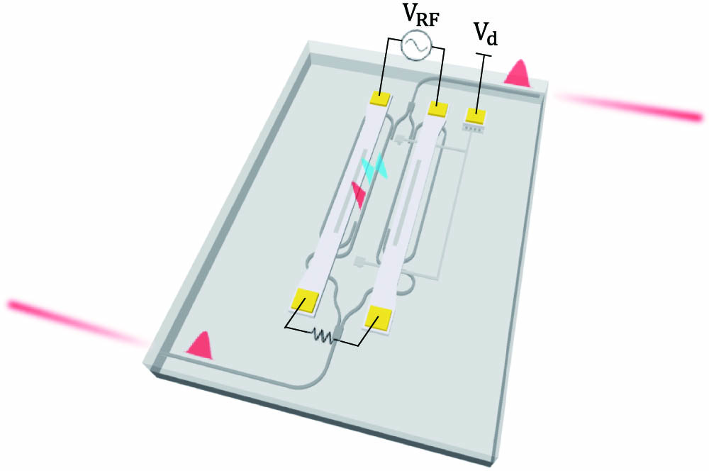
Figure 1.Schematic structure of the ML-MZM.
The operating principle of the modulator is depicted in Fig. 2(a). The input light is first split equally into two branches by the multimode interferometer (MMI) 3-dB power splitter and then propagates through the multimode waveguide in
![]()
Figure 2.(a) Operating principle of the proposed modulator; (b) cross section structure of the modulator arms.
Figure 2(b) shows the cross-sectional structure of the modulation arms. The multimode waveguide width is 840 nm, and the height is 220 nm with a 90-nm slab. The L-shaped PN junction is formed in the cross section of the multimode waveguide. The doping concentration is
For the proposed ML-MZM, the mode converter is of vital importance. A good mode converter should achieve mode conversion between
![]()
Figure 3.(a) Top view of the designed ADC mode converter; (b) simulated electric field of ADC; (c) calculated CE and XT of the mode converter.
Ideally, based on our original idea, the light will pass the phase shifter in the
![]()
Figure 4.(a) Refractive index variations for
To solve the problem mentioned above, the volume of the region in which the refractive index change occurs must be increased simultaneously with the waveguide width. In other words, a horizontally placed PN junction is necessary. We numerically compared the modulation efficiency of a single-mode waveguide and a two-mode waveguide with an L-shaped PN junction to verify this conclusion. As indicated, the depletion region of an L-shaped PN junction grows with the waveguide width for the two-mode waveguide. The refractive index variation result is shown in Fig. 4(d). The
3. DEVICE CHARACTERIZATION
Based on the aforementioned modulator design, the device is fabricated via a standard silicon photonic processing project provided by Advanced Micro Foundry (AMF). The top silicon layer is 220 nm, and the buried oxide thickness is 2 μm. The microscope image of the fabricated modulator is shown in Fig. 5.
![]()
Figure 5.Optical microscope image of (a) the fabricated ML-MZM, (b) the mode converter, (c) MMI.
The static transmission spectrum under different reverse bias voltages was first measured by using a broadband optical source and an optical spectrum analyzer (OSA); the result is shown in Fig. 6(a). The minimum transmission loss of the MZM is 24 dB (including 8 dB loss from the optical interface of the edge coupler), which mainly results from the large overlap between the optical mode field and the spatial charge region, especially for the
![]()
Figure 6.(a) Transmission spectra of the ML-MZM under different reverse voltages; (b) extracted phase change as a function of bias voltage.
In order to prove the improvement of the modulation efficiency, we fabricated the ML-MZM and a normal MZM on the same chip, as is shown in Figs. 7(a) and 7(b). Both of the devices have the same doping concentration and electrode structure. In comparison, the phase shifter length is 1 mm for the ML-MZM and 2 mm for the normal MZM. The transmission spectrum under different reverse bias voltages of the 2 mm normal MZM is shown in Fig. 7(c). We can see that the normal MZM has almost the same wavelength tuning spectra as the ML-MZM, which indicates the ML-MZM achieved the same phase shift with only half the size of a normal MZM, proving the doubled modulation efficiency, as expected by the concept.
![]()
Figure 7.(a) Microscope image of the ML-MZM with 1 mm phase shifter; (b) microscope image of the normal MZM with 2 mm phase shifter; (c) normal MZM transmission spectrum under various reverse voltages.
Then, we carried out the frequency response measurement of the proposed modulator in terms of the EO S parameter. A 43-GHz vector network analyzer (VNA, Anritsu, MS46322B) was utilized, and the measured S21 curve was normalized to 100 MHz. The EO S21 curve at a bias voltage of
![]()
Figure 8.Measured EO-S21 response at
A limited 3-dB EO bandwidth of about 5 GHz is obtained at
Figure 9(a) shows the experiment setup for high-speed modulation using the proposed modulator. A
![]()
Figure 9.(a) Schematic diagram of the high-speed measurement setup; (b) OOK eye diagram at 10 Gb/s; (c) OOK eye diagram at 15 Gb/s; (d) measured SNR response and bit allocation of 40 Gb/s DMT signal; (e) measured BER curve of 40 Gb/s DMT signal; (f) received constellations of four typical subcarriers of the DMT signal.
Therefore, a higher data rate can be expected by using DMT modulation format to adapt the channel response. The 40-Gb/s DMT signal with 160 subcarriers was mapped to 32 GHz bandwidth. The measured SNR response of the proposed device is plotted in Fig. 9(d). The Fischer algorithm was applied to calculate the bit allocation of the DMT signal, plotted by red circle symbols in Fig. 9(d); the calculated bit error rate (BER) curve is plotted in Fig. 9(e). The 40-Gb/s DMT signal has a BER under 7% forward-error-correction (FEC) threshold (3.8 × 10⁻³) at 3-dBm received optical power. The corresponding received constellations of the four typical subcarriers are depicted in Fig. 9(f).
To characterize the high-frequency response of the modulator, we also examine the generated peak sidebands that appear under the application of modulating RF signals. The sidebands are offset from the optical carrier by an equivalent modulation frequency (5 GHz per step). A single-frequency RF signal was generated by the AWG, and the modulated optical signal is directly fed into an OSA. The intensity of the modulation sidebands is recorded for each RF frequency, as shown in Fig. 10. It can be seen that the sideband power dropped significantly at 10 GHz and reached another peak at 20 GHz. The peaks of each modulation sideband are labeled in the red fit curve, which is in good agreement with the EO S21 curve in Fig. 8. Based on these results, we believe that the proposed ML-MZM can also be used for RF tone modulation applications like high-efficiency EO frequency comb generation, which needs rather high RF voltage for generating high-order sideband tones.
![]()
Figure 10.Optical modulation spectra of the modulator at different RF sinusoidal frequencies.
4. DISCUSSION
Table 1 compares our work with state-of-the-art high modulation efficiency carrier-depletion-based silicon MZMs. It can be seen that our work possesses the highest modulation efficiency with the lowest
Performance Comparison of Carrier-Depletion-Based Silicon Interferometric Modulator
| Reference | Structure | Operation Band | Bandwidth (GHz) | Speed (Gb/s) | |
|---|---|---|---|---|---|
| [ | MZM | C-band | 14.7 | 0.51 | 64 |
| [ | MZM | O-band | 13 | 0.46 | 24 |
| [ | MZM | C-band | 2.6 | 0.62 | 10 |
| [ | MZM | C-band | 12 | 0.81 | 10 |
| [ | MIM | C-band | 12 | 0.86 | 30 |
| [ | MIM | C-band | 11.3 | 0.72 | 40 |
| [ | MIM | C-band | 12 | 0.95 | 40 |
| This work | ML-MZM | C-band | 5 | 0.37 | 40 |
In our design, only
For the proposed ML-MZM, L is 1 mm and M is 2.69 mm. The calculated EO response of the proposed ML-MZM is shown in Fig. 11 with a red solid curve, which is consistent with the experiment result shown in Fig. 8. The velocity mismatch comes from the time delay of the racetrack loop-back waveguide, and it can be reduced by structures with shorter phase shifter length and smaller mode converter. Taking an ML-MZM with 0.5-mm phase shifter length as an example, the 3-dB EO bandwidth can be further increased to 11.3 GHz, as is shown in Fig. 11 by the blue dashed curve.
![]()
Figure 11.Calculated EO response of ML-MZM with 1 and 0.5 mm phase shifter length.
5. CONCLUSION
We proposed and experimentally demonstrated a silicon ML-MZM for recycled electric-optic modulation. High modulation efficiency with low
References
[1] A. Liu, R. Jones, L. Liao, D. Samara-Rubio, D. Rubin, O. Cohen, R. Nicolaescu, M. Paniccia. A high-speed silicon optical modulator based on a metal–oxide–semiconductor capacitor. Nature, 427, 615-618(2004).
[2] Y. Ogiso, J. Ozaki, Y. Ueda, N. Kashio, N. Kikuchi, E. Yamada, H. Tanobe, S. Kanazawa, H. Yamazaki, Y. Ohiso, T. Fujii, M. Kohtoku. Over 67 GHz bandwidth and 1.5 V
[3] S. Wolf, H. Zwickel, C. Kieninger, M. Lauermann, W. Hartmann, Y. Kutuvantavida, W. Freude, S. Randel, C. Koos. Coherent modulation up to 100 GBd 16QAM using silicon-organic hybrid (SOH) devices. Opt. Express, 26, 220-232(2018).
[4] M. Ayata, Y. Fedoryshyn, W. Heni, B. Baeuerle, A. Josten, M. Zahner, U. Koch, Y. Salamin, C. Hoessbacher, C. Haffner, D. L. Elder, L. R. Dalton, J. Leuthold. High-speed plasmonic modulator in a single metal layer. Science, 358, 630-632(2017).
[5] C. Wang, M. Zhang, X. Chen, M. Bertrand, A. Shams-Ansari, S. Chandrasekhar, P. Winzer, M. Lončar. Integrated lithium niobate electro-optic modulators operating at CMOS-compatible voltages. Nature, 562, 101-104(2018).
[6] G. T. Reed, G. Mashanovich, F. Y. Gardes, D. Thomson. Silicon optical modulators. Nat. Photonics, 4, 518-526(2010).
[7] A. Rahim, A. Hermans, B. Wohlfeil, D. Petousi, B. Kuyken, D. Van Thourhout, R. Baets. Taking silicon photonics modulators to a higher performance level: state-of-the-art and a review of new technologies. Adv. Photon., 3, 024003(2021).
[8] J. Sun, R. Kumar, M. Sakib, J. B. Driscoll, H. Jayatilleka, H. Rong. A 128 Gb/s PAM4 silicon microring modulator with integrated thermo-optic resonance tuning. J. Lightwave Technol., 37, 110-115(2019).
[9] H. Zhang, M. Li, Y. Zhang, D. Zhang, Q. Liao, J. He, S. Hu, B. Zhang, L. Wang, X. Xiao, N. Qi, S. Yu. 800 Gbit/s transmission over 1 km single-mode fiber using a four-channel silicon photonic transmitter. Photon. Res., 8, 1776-1782(2020).
[10] M. Jacques, Z. Xing, A. Samani, E. El-Fiky, X. Li, M. Xiang, S. Lessard, D. V. Plant. 240 Gbit/s silicon photonic Mach-Zehnder modulator enabled by two 2.3-Vpp drivers. J. Lightwave Technol., 38, 2877-2885(2020).
[11] G. Zhou, L. Zhou, Y. Guo, S. Chen, L. Lu, L. Liu, J. Chen. 32-Gb/s OOK and 64-Gb/s PAM-4 modulation using a single-drive silicon Mach–Zehnder modulator with 2 V drive voltage. IEEE Photon. J., 11, 6603610(2019).
[12] Z. Yong, W. D. Sacher, Y. Huang, J. C. Mikkelsen, Y. Yang, X. Luo, P. Dumais, D. Goodwill, H. Bahrami, P. G.-Q. Lo, E. Bernier, J. K. S. Poon. U-shaped PN junctions for efficient silicon Mach-Zehnder and microring modulators in the O-band. Opt. Express, 25, 8425-8439(2017).
[13] H. Yu, M. Pantouvaki, J. V. Campenhout, D. Korn, K. Komorowska, P. Dumon, Y. Li, P. Verheyen, P. Absil, L. Alloatti, D. Hillerkuss, J. Leuthold, R. Baets, W. Bogaerts. Performance tradeoff between lateral and interdigitated doping patterns for high speed carrier-depletion based silicon modulators. Opt. Express, 20, 12926-12938(2012).
[14] K. Goi, N. Ishikura, H. Ishihara, S. Sakamoto, K. Ogawa, T.-Y. Liow, X. Tu, G.-Q. Lo, D.-L. Kwong. Low-voltage silicon Mach-Zehnder modulator operating at high temperatures without thermo-electric cooling. Optical Fiber Communication Conference, W2A-23(2016).
[15] D. Patel, V. Veerasubramanian, S. Ghosh, A. Samani, Q. Zhong, D. V. Plant. High-speed compact silicon photonic Michelson interferometric modulator. Opt. Express, 22, 26788-26802(2014).
[16] X. Li, X. Xiao, H. Xu, Z. Li, T. Chu, J. Yu, Y. Yu. Highly efficient silicon Michelson interferometer modulators. IEEE Photon. Technol. Lett., 25, 407-409(2013).
[17] M. Wang, L. Zhou, H. Zhu, Y. Zhou, Y. Zhong, J. Chen. Low-loss high-extinction-ratio single-drive push-pull silicon Michelson interferometric modulator. Chin. Opt. Lett., 15, 042501(2017).
[18] M. Lipson, S. A. Miller, C. T. Phare, Y.-C. Chang, X. Ji, O. A. J. Gordillo, A. Mohanty, S. P. Roberts, M. C. Shin, B. Stern, M. Zadka. Silicon photonics integration for future generation optical network. European Conference on Optical Communication (ECOC), 1-2(2018).
[19] X. Huang, Y. Liu, Z. Li, H. Guan, Q. Wei, M. Tan, Z. Li. 40 GHz high-efficiency Michelson interferometer modulator on a silicon-rich nitride and thin-film lithium niobate hybrid platform. Opt. Lett., 46, 2811-2814(2021).
[20] J. Jian, M. Xu, L. Liu, Y. Luo, J. Zhang, L. Liu, L. Zhou, H. Chen, S. Yu, X. Cai. High modulation efficiency lithium niobate Michelson interferometer modulator. Opt. Express, 27, 18731-18739(2019).


Set citation alerts for the article
Please enter your email address

© Copyright 2018-2021 | Chinese Laser Press. All Rights Reserved 沪ICP备15018463号-20