Contents


2022
Volume: 10 Issue 7
27 Article(s)
Export citation format
NEXT-GENERATION SILICON PHOTONICS
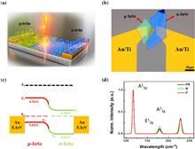
Self-driven highly responsive p-n junction InSe heterostructure near-infrared light detector
Chandraman Patil, Chaobo Dong, Hao Wang, Behrouz Movahhed Nouri... and Volker J. Sorger|Show fewer author(s)
Photodetectors converting light signals into detectable photocurrents are ubiquitously in use today. To improve the compactness and performance of next-generation devices and systems, low dimensional materials provide rich physics to engineering the light–matter interaction. Photodetectors based on two-dimensional (2D) material van der Waals heterostructures have shown high responsivity and compact integration capability, mainly in the visible range due to their intrinsic bandgap. The spectral region of near-infrared (NIR) is technologically important, featuring many data communication and sensing applications. While some initial NIR 2D material-based detectors have emerged, demonstrations of doping-junction-based 2D material photodetectors with the capability to harness the charge-separation photovoltaic effect are yet outstanding. Here, we demonstrate a 2D p-n van der Waals heterojunction photodetector constructed by vertically stacking p-type and n-type indium selenide (InSe) flakes. This heterojunction charge-separation-based photodetector shows a threefold enhancement in responsivity in the NIR spectral region (980 nm) as compared to photoconductor detectors based on p- or n-only doped InSe. We show that this junction device exhibits self-powered photodetection operation, exhibits few pA-low dark currents, and is about 3–4 orders of magnitude more efficient than the state-of-the-art foundry-based devices. Such capability opens doors for low noise and low photon flux photodetectors that do not rely on external gain. We further demonstrate millisecond response rates in this sensitive zero-bias voltage regime. Such sensitive photodetection capability in the technologically relevant NIR wavelength region at low form factors holds promise for several applications including wearable biosensors, three-dimensional (3D) sensing, and remote gas sensing.Photodetectors converting light signals into detectable photocurrents are ubiquitously in use today. To improve the compactness and performance of next-generation devices and systems, low dimensional materials provide rich physics to engineering the light–matter interaction. Photodetectors based on two-dimensional (2D) material van der Waals heterostructures have shown high responsivity and compact integration capability, mainly in the visible range due to their intrinsic bandgap. The spectral region of near-infrared (NIR) is technologically important, featuring many data communication and sensing applications. While some initial NIR 2D material-based detectors have emerged, demonstrations of doping-junction-based 2D material photodetectors with the capability to harness the charge-separation photovoltaic effect are yet outstanding. Here, we demonstrate a 2D p-n van der Waals heterojunction photodetector constructed by vertically stacking p-type and n-type indium selenide (InSe) flakes. This heterojunction charge-separation-based photodetector shows a threefold enhancement in responsivity in the NIR spectral region (980 nm) as compared to photoconductor detectors based on p- or n-only doped InSe. We show that this junction device exhibits self-powered photodetection operation, exhibits few pA-low dark currents, and is about 3–4 orders of magnitude more efficient than the state-of-the-art foundry-based devices. Such capability opens doors for low noise and low photon flux photodetectors that do not rely on external gain. We further demonstrate millisecond response rates in this sensitive zero-bias voltage regime. Such sensitive photodetection capability in the technologically relevant NIR wavelength region at low form factors holds promise for several applications including wearable biosensors, three-dimensional (3D) sensing, and remote gas sensing..
Photonics Research
- Publication Date: Jun. 30, 2022
- Vol. 10, Issue 7, A97 (2022)


Research Articles
Fiber Optics and Optical Communications
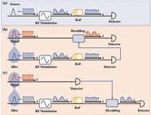
Quantum microwave photonics in radio-over-fiber systems
Yaqing Jin, Ye Yang, Huibo Hong, Xiao Xiang... and Ruifang Dong|Show fewer author(s)
As the main branch of microwave photonics, radio-over-fiber technology provides high bandwidth, low-loss, and long-distance propagation capability, facilitating wide applications ranging from telecommunication to wireless networks. With ultrashort pulses as the optical carrier, a large capacity is further endowed. However, the wide bandwidth of ultrashort pulses results in the severe vulnerability of high-frequency radio frequency (RF) signals to fiber dispersion. With a time-energy entangled biphoton source as the optical carrier combined with the single-photon detection technique, a quantum microwave photonics method in radio-over-fiber systems is proposed and demonstrated experimentally. The results show that it not only realizes unprecedented nonlocal RF signal modulation with strong resistance to the dispersion but also provides an alternative mechanism to distill the RF signal out from the dispersion effectively. Furthermore, the spurious-free dynamic ranges of the nonlocally modulated and distilled RF signals have been significantly improved. With the ultra-weak detection and the high-speed processing advantages endowed by the low-timing-jitter single-photon detection, the quantum microwave photonics method opens new possibilities in modern communication and networks.As the main branch of microwave photonics, radio-over-fiber technology provides high bandwidth, low-loss, and long-distance propagation capability, facilitating wide applications ranging from telecommunication to wireless networks. With ultrashort pulses as the optical carrier, a large capacity is further endowed. However, the wide bandwidth of ultrashort pulses results in the severe vulnerability of high-frequency radio frequency (RF) signals to fiber dispersion. With a time-energy entangled biphoton source as the optical carrier combined with the single-photon detection technique, a quantum microwave photonics method in radio-over-fiber systems is proposed and demonstrated experimentally. The results show that it not only realizes unprecedented nonlocal RF signal modulation with strong resistance to the dispersion but also provides an alternative mechanism to distill the RF signal out from the dispersion effectively. Furthermore, the spurious-free dynamic ranges of the nonlocally modulated and distilled RF signals have been significantly improved. With the ultra-weak detection and the high-speed processing advantages endowed by the low-timing-jitter single-photon detection, the quantum microwave photonics method opens new possibilities in modern communication and networks..
Photonics Research
- Publication Date: Jun. 30, 2022
- Vol. 10, Issue 7, 1669 (2022)
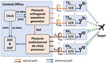
Photonics-enabled distributed MIMO radar for high-resolution 3D imaging
Jingwen Dong, Qiang Sun, Zekun Jiao, Liqi Zhang... and Wangzhe Li|Show fewer author(s)
Three-dimensional (3D) imaging radar is an advanced sensor applied in space surveillance and target recognition for supplying 3D geometric features and supporting visualization. However, high 3D resolution requires both broadband operation and a large 2D aperture, which are difficult and complex for conventional radars. This paper presents a photonics-enabled distributed multiple-input and multiple-output (MIMO) radar with a centralized architecture. By use of photonic multi-dimensional multiplexing, multi-channel signal generation and reception are implemented on a shared reference signal in a central office, enabling a highly coherent network with a simple structure. Additionally, a sparse array and a synthetic aperture are combined to efficiently reduce the required transceivers, further weakening the dilemma between system complexity and angular resolution. A 4×4 MIMO radar is established and evaluated in field tests. A high-resolution 3D image of a non-cooperative aircraft is obtained, in which rich details are displayed. From a comparison with electronics-based radar, significant resolution improvement is observed. The results verify the superior imaging capability and practicability of the proposed radar and its great potential to outperform conventional technologies in target classification and recognition applications.Three-dimensional (3D) imaging radar is an advanced sensor applied in space surveillance and target recognition for supplying 3D geometric features and supporting visualization. However, high 3D resolution requires both broadband operation and a large 2D aperture, which are difficult and complex for conventional radars. This paper presents a photonics-enabled distributed multiple-input and multiple-output (MIMO) radar with a centralized architecture. By use of photonic multi-dimensional multiplexing, multi-channel signal generation and reception are implemented on a shared reference signal in a central office, enabling a highly coherent network with a simple structure. Additionally, a sparse array and a synthetic aperture are combined to efficiently reduce the required transceivers, further weakening the dilemma between system complexity and angular resolution. A
Photonics Research
- Publication Date: Jun. 30, 2022
- Vol. 10, Issue 7, 1679 (2022)
Imaging Systems, Microscopy, and Displays
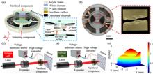
Ultra-wide varifocal imaging with selectable region of interest capacity using Alvarez lenses actuated by a dielectric elastomer
Qun Hao, Chuanxun Chen, Jie Cao, Zhikuo Li, and Yang Cheng
A remarkable feature of Alvarez lenses is that a wide focal length tuning range can be achieved using lateral displacement rather than commonly used axial translation, thus, reducing the overall length of varifocal imaging systems. Here, we present novel lens elements based on Alvarez lenses actuated by a dielectric elastomer (DE). The proposed lens elements are composed of the varifocal component and the scanning component. Based on the proposed lens elements, an imaging system is built to realize ultra-wide varifocal imaging with a selectable region of interest. The lens elements have a variable focus function based on an Alvarez lens structure and a DE actuator and a scanning function based on the DE-based four-quadrant actuators. The large deformation generated by the DE actuators permits the lateral displacement of the Alvarez lenses up to 1.145 mm. The focal length variation of the proposed varifocal component is up to 30.5 times, where the maximum focal length is 181 mm and the minimum focal length is 5.94 mm. The rise and fall times of the varifocal component are 160 ms and 295 ms, respectively. By applying different voltages on four-quadrant actuators, the scanning component allows the varifocal component to move in different directions and endows the varifocal component with a selectable region of interest imaging capability. The scanning range of the scanning component is 17.57°. The imaging resolution of the imaging system is approximately 181 lp/mm. The system developed in the current study has the potential to be used in consumer electronics, endoscopy, and microscopy in the future.A remarkable feature of Alvarez lenses is that a wide focal length tuning range can be achieved using lateral displacement rather than commonly used axial translation, thus, reducing the overall length of varifocal imaging systems. Here, we present novel lens elements based on Alvarez lenses actuated by a dielectric elastomer (DE). The proposed lens elements are composed of the varifocal component and the scanning component. Based on the proposed lens elements, an imaging system is built to realize ultra-wide varifocal imaging with a selectable region of interest. The lens elements have a variable focus function based on an Alvarez lens structure and a DE actuator and a scanning function based on the DE-based four-quadrant actuators. The large deformation generated by the DE actuators permits the lateral displacement of the Alvarez lenses up to 1.145 mm. The focal length variation of the proposed varifocal component is up to 30.5 times, where the maximum focal length is 181 mm and the minimum focal length is 5.94 mm. The rise and fall times of the varifocal component are 160 ms and 295 ms, respectively. By applying different voltages on four-quadrant actuators, the scanning component allows the varifocal component to move in different directions and endows the varifocal component with a selectable region of interest imaging capability. The scanning range of the scanning component is 17.57°. The imaging resolution of the imaging system is approximately 181 lp/mm. The system developed in the current study has the potential to be used in consumer electronics, endoscopy, and microscopy in the future..
Photonics Research
- Publication Date: Jun. 10, 2022
- Vol. 10, Issue 7, 1543 (2022)
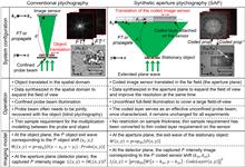
Synthetic aperture ptychography: coded sensor translation for joint spatial-Fourier bandwidth expansion | Editors' Pick
Pengming Song, Shaowei Jiang, Tianbo Wang, Chengfei Guo... and Guoan Zheng|Show fewer author(s)
Conventional ptychography translates an object through a localized probe beam to widen the field of view in real space. Fourier ptychography translates the object spectrum through a pupil aperture to expand the Fourier bandwidth in reciprocal space. Here we report an imaging modality, termed synthetic aperture ptychography (SAP), to get the best of both techniques. In SAP, we illuminate a stationary object using an extended plane wave and translate a coded image sensor at the far field for data acquisition. The coded layer attached on the sensor modulates the object exit waves and serves as an effective ptychographic probe for phase retrieval. The sensor translation process in SAP synthesizes a large complex-valued wavefront at the intermediate aperture plane. By propagating this wavefront back to the object plane, we can widen the field of view in real space and expand the Fourier bandwidth in reciprocal space simultaneously. We validate the SAP approach with transmission targets and reflection silicon microchips. A 20-mm aperture was synthesized using a 5-mm sensor, achieving a fourfold gain in resolution and 16-fold gain in field of view for object recovery. In addition, the thin sample requirement in ptychography is no longer required in SAP. One can digitally propagate the recovered exit wave to any axial position for post-acquisition refocusing. The SAP scheme offers a solution for far-field sub-diffraction imaging without using lenses. It can be adopted in coherent diffraction imaging setups with radiation sources from visible light, extreme ultraviolet, and X-ray, to electron.Conventional ptychography translates an object through a localized probe beam to widen the field of view in real space. Fourier ptychography translates the object spectrum through a pupil aperture to expand the Fourier bandwidth in reciprocal space. Here we report an imaging modality, termed synthetic aperture ptychography (SAP), to get the best of both techniques. In SAP, we illuminate a stationary object using an extended plane wave and translate a coded image sensor at the far field for data acquisition. The coded layer attached on the sensor modulates the object exit waves and serves as an effective ptychographic probe for phase retrieval. The sensor translation process in SAP synthesizes a large complex-valued wavefront at the intermediate aperture plane. By propagating this wavefront back to the object plane, we can widen the field of view in real space and expand the Fourier bandwidth in reciprocal space simultaneously. We validate the SAP approach with transmission targets and reflection silicon microchips. A 20-mm aperture was synthesized using a 5-mm sensor, achieving a fourfold gain in resolution and 16-fold gain in field of view for object recovery. In addition, the thin sample requirement in ptychography is no longer required in SAP. One can digitally propagate the recovered exit wave to any axial position for post-acquisition refocusing. The SAP scheme offers a solution for far-field sub-diffraction imaging without using lenses. It can be adopted in coherent diffraction imaging setups with radiation sources from visible light, extreme ultraviolet, and X-ray, to electron..
Photonics Research
- Publication Date: Jun. 21, 2022
- Vol. 10, Issue 7, 1624 (2022)

Imaging through scattering media via spatial–temporal encoded pattern illumination
Xingchen Zhao, Xiaoyu Nie, Zhenhuan Yi, Tao Peng, and Marlan O. Scully
Optical imaging through scattering media has long been a challenge. Many approaches have been developed for focusing light or imaging objects through scattering media, but usually, they are either invasive, limited to stationary or slow-moving media, or require high-resolution cameras and complex algorithms to retrieve the images. By utilizing spatial–temporal encoded patterns (STEPs), we introduce a technique for the computation of imaging that overcomes these restrictions. With a single-pixel photodetector, we demonstrate non-invasive imaging through scattering media. This technique is insensitive to the motion of the media. Furthermore, we demonstrate that our image reconstruction algorithm is much more efficient than correlation-based algorithms for single-pixel imaging, which may allow fast imaging for applications with limited computing resources.Optical imaging through scattering media has long been a challenge. Many approaches have been developed for focusing light or imaging objects through scattering media, but usually, they are either invasive, limited to stationary or slow-moving media, or require high-resolution cameras and complex algorithms to retrieve the images. By utilizing spatial–temporal encoded patterns (STEPs), we introduce a technique for the computation of imaging that overcomes these restrictions. With a single-pixel photodetector, we demonstrate non-invasive imaging through scattering media. This technique is insensitive to the motion of the media. Furthermore, we demonstrate that our image reconstruction algorithm is much more efficient than correlation-based algorithms for single-pixel imaging, which may allow fast imaging for applications with limited computing resources..
Photonics Research
- Publication Date: Jun. 30, 2022
- Vol. 10, Issue 7, 1689 (2022)

Adaptive optics wavefront correction using a damped transpose matrix of the influence function
Boyu Gu, and Yuhua Zhang
To assess the performance of adaptive optics and predict an optimal wavefront correction, we built a wavefront reconstructor with a damped transpose matrix of the influence function. Using an integral control strategy, we tested this reconstructor with four deformable mirrors in an experimental system, an adaptive optics scanning laser ophthalmoscope, and an adaptive optics near-confocal ophthalmoscope. Testing results proved that this reconstructor could ensure a stable and precise correction for wavefront aberration compared to a conventional optimal reconstructor formed by the inverse matrix of the influence function. This method may provide a helpful tool for testing, evaluating, and optimizing adaptive optics systems.To assess the performance of adaptive optics and predict an optimal wavefront correction, we built a wavefront reconstructor with a damped transpose matrix of the influence function. Using an integral control strategy, we tested this reconstructor with four deformable mirrors in an experimental system, an adaptive optics scanning laser ophthalmoscope, and an adaptive optics near-confocal ophthalmoscope. Testing results proved that this reconstructor could ensure a stable and precise correction for wavefront aberration compared to a conventional optimal reconstructor formed by the inverse matrix of the influence function. This method may provide a helpful tool for testing, evaluating, and optimizing adaptive optics systems..
Photonics Research
- Publication Date: Jun. 30, 2022
- Vol. 10, Issue 7, 1777 (2022)
Instrumentation and Measurements
Simultaneous multiple time scale imaging for kHz–MHz high-speed accelerometry | Spotlight on Optics
Vassily Kornienko, David Andersson, Mehdi Stiti, Jonas Ravelid... and Elias Kristensson|Show fewer author(s)
Fast transient events, such as the disintegration of liquid bodies or chemical reactions between radical species, involve various processes that may occur at different time scales. Currently, there are two alternatives for monitoring such events: burst- or high-speed imaging. Burst imaging at ultrahigh speeds (∼100 MHz to THz) allows for the capture of nature’s fastest processes but only for a narrowly confined period of time and at a repetition rate of ∼10 Hz. Monitoring long lasting, rapidly evolving transient events requires a significantly higher repetition rate, which is met by existing ∼kHz to 1 MHz high-speed imaging technology. However, the use of such systems eliminates the possibility to observe dynamics occurring on the sub-microsecond time scale. In this paper, we present a solution to this technological gap by combining multiplexed imaging with high-speed sensor technology, resulting in temporally resolved, high-spatial-resolution image series at two simultaneous time scales. We further demonstrate how the collection of such data opens up the tracking of rapidly evolving structures up to MHz burst rates over long durations, allowing, for the first time, to our knowledge, the extraction of acceleration fields acting upon the liquid bodies of an atomizing spray in two dimensions at kHz frame rates.Fast transient events, such as the disintegration of liquid bodies or chemical reactions between radical species, involve various processes that may occur at different time scales. Currently, there are two alternatives for monitoring such events: burst- or high-speed imaging. Burst imaging at ultrahigh speeds (
Photonics Research
- Publication Date: Jun. 30, 2022
- Vol. 10, Issue 7, 1712 (2022)
Integrated Optics
On-chip path encoded photonic quantum Toffoli gate | On the Cover
Meng Li, Chu Li, Yang Chen, Lan-Tian Feng... and Yan Li|Show fewer author(s)
The quantum Toffoli gate is one of the most important three-qubit gates, but it is challenging to construct a chip according to the complicated traditional circuit. Using the optimized 3D configuration with an overpass waveguide to reduce the circuit complexity, we successfully fabricate an on-chip path encoded photonic quantum Toffoli gate enabled by the 3D capability of the femtosecond laser direct writing (FLDW) for the first time to our knowledge, whose truth-table fidelity is higher than 85.5%. Furthermore, a path encoded four-qubit controlled-controlled-controlled NOT gate is written to confirm the scalability of this resource-saving technique. This work paves the way for the FLDW of more complex and powerful photonic quantum computation chips.The quantum Toffoli gate is one of the most important three-qubit gates, but it is challenging to construct a chip according to the complicated traditional circuit. Using the optimized 3D configuration with an overpass waveguide to reduce the circuit complexity, we successfully fabricate an on-chip path encoded photonic quantum Toffoli gate enabled by the 3D capability of the femtosecond laser direct writing (FLDW) for the first time to our knowledge, whose truth-table fidelity is higher than 85.5%. Furthermore, a path encoded four-qubit controlled-controlled-controlled NOT gate is written to confirm the scalability of this resource-saving technique. This work paves the way for the FLDW of more complex and powerful photonic quantum computation chips..
Photonics Research
- Publication Date: Jun. 09, 2022
- Vol. 10, Issue 7, 1533 (2022)
Improving long-term temperature bias stability of an integrated optical gyroscope employing a Si3N4 resonator
Changkun Feng, Yonggui Zhang, Honghao Ma, Hui Li, and Lishuang Feng
The presence of polarization noise generated by the waveguide resonator limits the performance of a resonant integrated optical gyroscope (RIOG). Using silicon nitride (Si3N4) to fabricate a waveguide with an ultralow-aspect-ratio can result in a resonator that only supports light transmission in a single-polarization state, suppressing polarization noise. We successfully fabricated a Si3N4 resonator with a bending radius of 17.5 mm, a finesse (F) of 150, a quality factor (Q) of 1.54×10⁷, and a propagation loss of 1.2 dB/m. The Si3N4 resonator was used to construct a double closed-loop RIOG that showed long-term bias stability (3600 s) of 13.2°/h at room temperature, 14.8°/h at 40°C, 21.2°/h at 50°C, and 23.6°/h at 60°C. We believe this to be the best performance reported to date for a Si3N4 resonator-based RIOG. This advancement paves the way for the wider application of RIOGs.The presence of polarization noise generated by the waveguide resonator limits the performance of a resonant integrated optical gyroscope (RIOG). Using silicon nitride (
Photonics Research
- Publication Date: Jun. 30, 2022
- Vol. 10, Issue 7, 1661 (2022)
Lasers and Laser Optics
Lanthanide-doped nanocrystals in high-Q microtoroids for stable on-chip white-light lasers
Limin Jin, Zhuo Liu, Yuqi Zhang, Yunkai Wu... and Shumin Xiao|Show fewer author(s)
The plentiful energy states of lanthanide (Ln3+)-doped nanomaterials make them very promising for on-chip integrated white-light lasers. Despite the rapid progresses, the Ln3+-based white upconversion emissions are strongly restricted by their low upconversion quantum efficiency and the color stability. Herein, we combine the CaF2:Yb35Tm1.5Er0.5 nanocrystals and the high-Q microtoroids, and experimentally demonstrate the chip-integrated stable white-light laser. By optimizing the sizes, density, and distributions of Ln3+-doped nanocrystals, the Q factors of Ln3+-doped microtoroids are maintained as high as 5×10⁵. The strong light matter interaction in high-Q microtoroids greatly enhances the upconversion emission and dramatically reduces the laser thresholds at 652 nm, 545 nm, and 475 nm to similarly low values (1.89–2.10 mJ cm-2). Consequently, robust white-light microlaser has been experimentally achieved from a single microtoroid. This research has paved a solid step toward the chip-scale integrated broadband microlasers.The plentiful energy states of lanthanide (
Photonics Research
- Publication Date: Jun. 14, 2022
- Vol. 10, Issue 7, 1594 (2022)
Nanophotonics and Photonic Crystals
1D quasi-bound states in the continuum with large operation bandwidth in the
Kaili Sun, Hui Jiang, Dmitry A. Bykov, Vien Van... and Zhanghua Han|Show fewer author(s)
The phenomenon of bound state in the continuum (BIC) with an infinite quality factor and lifetime has emerged in recent years in photonics as a new tool to manipulate light–matter interactions. However, most of the investigated structures only support BIC resonances at very few discrete points in the ω∼k space. Even when the BIC is switched to a quasi-BIC (QBIC) resonance through perturbation, its frequency will still be located within a narrow spectral band close to that of the original BIC, restricting their applications in many fields where random or multiple input frequencies beyond the narrow band are required. In this work, we demonstrate that a new set of QBIC resonances can be supported by using a special binary grating consisting of two alternatingly aligned ridge arrays with the same period and zero-approaching ridge width difference on a slab waveguide. These QBIC resonances are distributed continuously over a broad band along a line in the ω∼k space and can thus be considered as 1D QBICs. With the Q factors generally affected by the ridge difference, it is now possible to arbitrarily choose any frequencies on the dispersion line to achieve significantly enhanced light–matter interactions, facilitating many applications where multiple input wavelengths are required; e.g., sum or difference frequency generations in nonlinear optics.The phenomenon of bound state in the continuum (BIC) with an infinite quality factor and lifetime has emerged in recent years in photonics as a new tool to manipulate light–matter interactions. However, most of the investigated structures only support BIC resonances at very few discrete points in the
Photonics Research
- Publication Date: Jun. 14, 2022
- Vol. 10, Issue 7, 1575 (2022)
Boosting anapole-exciton strong coupling in all-dielectric heterostructures
Jingyu Wang, Weimin Yang, Guoya Sun, Yonglin He... and Zhilin Yang|Show fewer author(s)
The light manipulation beyond the diffraction limit plays an invaluable role in modern physics and nanophotonics. In this work, we have demonstrated a strong coupling with a large Rabi splitting of 151 meV between bulk WS2 excitons and anapole modes in the WS2-Si nanodisk heterostructure array with nanoholes as small as 50 nm radius. This result is acquired by introducing anapole modes to suppress radiative losses to confine light into subwavelength volumes and large spatial overlapping between excitons and strong optical fields. Our work shows that anapole modes may serve as a powerful way to enhance the interaction between light and matter at nanoscales, and it should pave an avenue toward high-performance all-dielectric optoelectronic applications.The light manipulation beyond the diffraction limit plays an invaluable role in modern physics and nanophotonics. In this work, we have demonstrated a strong coupling with a large Rabi splitting of 151 meV between bulk
Photonics Research
- Publication Date: Jun. 30, 2022
- Vol. 10, Issue 7, 1744 (2022)
Nonlinear Optics
Nonlinear quantum spectroscopy with parity–time-symmetric integrated circuits
Pawan Kumar, Sina Saravi, Thomas Pertsch, Frank Setzpfandt, and Andrey A. Sukhorukov
We propose a novel quantum nonlinear interferometer design that incorporates a passive parity–time (PT)-symmetric coupler sandwiched between two nonlinear sections where signal–idler photon pairs are generated. The PT symmetry enables efficient coupling of the longer-wavelength idler photons and facilitates the sensing of losses in the second waveguide exposed to analyte under investigation, whose absorption can be inferred by measuring only the signal intensity at a shorter wavelength where efficient detectors are readily available. Remarkably, we identify a new phenomenon of sharp signal intensity fringe shift at critical idler loss values, which is distinct from the previously studied PT symmetry breaking. We discuss how such unconventional properties arising from quantum interference can provide a route to enhancing the sensing of analytes and facilitate broadband spectroscopy applications in integrated photonic platforms.We propose a novel quantum nonlinear interferometer design that incorporates a passive parity–time (PT)-symmetric coupler sandwiched between two nonlinear sections where signal–idler photon pairs are generated. The PT symmetry enables efficient coupling of the longer-wavelength idler photons and facilitates the sensing of losses in the second waveguide exposed to analyte under investigation, whose absorption can be inferred by measuring only the signal intensity at a shorter wavelength where efficient detectors are readily available. Remarkably, we identify a new phenomenon of sharp signal intensity fringe shift at critical idler loss values, which is distinct from the previously studied PT symmetry breaking. We discuss how such unconventional properties arising from quantum interference can provide a route to enhancing the sensing of analytes and facilitate broadband spectroscopy applications in integrated photonic platforms..
Photonics Research
- Publication Date: Jun. 30, 2022
- Vol. 10, Issue 7, 1763 (2022)
Optical and Photonic Materials
Nonvolatile reconfigurable dynamic Janus metasurfaces in the terahertz regime
Shoujun Zhang, Xieyu Chen, Kuan Liu, Haiyang Li... and Zhen Tian|Show fewer author(s)
Metasurfaces, especially tunable ones, have played a major role in controlling the amplitude, phase, and polarization of electromagnetic waves and attracted growing interest, with a view toward a new generation of miniaturized devices. However, to date, most existing reconfigurable devices are bounded in volatile nature with sustained external energy to maintain and single functionality, which restrict their further applications. Here, we demonstrate for the first time, to our knowledge, nonvolatile, reconfigurable, and dynamic Janus metasurfaces by incorporating phase-change material Ge2Se2Te5 (GST) in the terahertz (THz) regime. First, we experimentally show the reversible switching characteristic of GST on large areas by applying a single nanosecond laser pulse, which exhibits excellent contrast of THz properties in both states. Then, we present a multiplex metasurface scheme. In each metasurface, three sets of structures are adopted, in which two sets integrate GST. The effective structures can be reversely modulated by the amorphization and crystallization of GST. As a proof of concept, the dynamic beam splitter, bifocal metalens, dual-mode focusing optical vortex generators, and switchable metalens/focusing optical vortex generators are designed, fabricated, and experimentally characterized, and can be switched reversibly and repeatedly with the help of optical and thermal stimuli. Our scheme will pave the way toward the development of multifunctional and compact THz devices and may find use for applications in THz imaging, sensing, and communications.Metasurfaces, especially tunable ones, have played a major role in controlling the amplitude, phase, and polarization of electromagnetic waves and attracted growing interest, with a view toward a new generation of miniaturized devices. However, to date, most existing reconfigurable devices are bounded in volatile nature with sustained external energy to maintain and single functionality, which restrict their further applications. Here, we demonstrate for the first time, to our knowledge, nonvolatile, reconfigurable, and dynamic Janus metasurfaces by incorporating phase-change material
Photonics Research
- Publication Date: Jun. 30, 2022
- Vol. 10, Issue 7, 1731 (2022)
Optical Devices
All dielectric metasurfaces for spin-dependent terahertz wavefront control
Tong Wu, Huifang Zhang, Sivaloganathan Kumaran, Yuehong Xu... and Jiaguang Han|Show fewer author(s)
Metasurfaces consisting of artificial subwavelength structure arrays have shown unprecedented ability to manipulate the phase, amplitude, and polarization of light. Separate and complete control over different spin states, namely the orthogonal circular polarizations, has proven more challenging as compared to the control over orthogonal linear polarizations. Here, we present and experimentally demonstrate several spin-dependent wavefront control metasurfaces in the terahertz regime using all-silicon dielectric structures. Such spin-dependent all-silicon metasurfaces are easy to fabricate and have potential applications in spin-involved ultracompact and miniaturized terahertz optical systems as well as terahertz communication systems.Metasurfaces consisting of artificial subwavelength structure arrays have shown unprecedented ability to manipulate the phase, amplitude, and polarization of light. Separate and complete control over different spin states, namely the orthogonal circular polarizations, has proven more challenging as compared to the control over orthogonal linear polarizations. Here, we present and experimentally demonstrate several spin-dependent wavefront control metasurfaces in the terahertz regime using all-silicon dielectric structures. Such spin-dependent all-silicon metasurfaces are easy to fabricate and have potential applications in spin-involved ultracompact and miniaturized terahertz optical systems as well as terahertz communication systems..
Photonics Research
- Publication Date: Jun. 30, 2022
- Vol. 10, Issue 7, 1695 (2022)
Optoelectronics
Creation of cylindrical vector beams through highly anisotropic scattering media with a single scalar transmission matrix calibration
Qian Zhao, Shijie Tu, Qiannan Lei, Chengshan Guo... and Yangjian Cai|Show fewer author(s)
Cylindrical vector (CV) beams have attracted increasing interest due to their particular properties and their applications in optical imaging, optical manipulation, and light–matter interactions. However, it is challenging to construct CV beams through highly anisotropic scattering media (HASM), such as thick biological tissue, posing a barrier to the applications of CV beams that involve HASM. Here, we present a scheme to construct CV beams beyond high scattering that only requires a single scalar transmission matrix (TM) calibration and manipulation of the spatial degrees of freedom of the scalar input field. Assisted by a radial polarization converter (S-waveplate) and a polarizer, the scheme enables one to obtain the correct incident wavefront for the creation of CV beams through HASM with only one single scalar TM calibration. Compared to the existing method, this user-friendly approach is fast and simple in terms of the optical implements and computations. Both radially and azimuthally polarized beams are experimentally constructed through a ZnO scattering layer to demonstrate the viability of the method. Arbitrarily generalized CV beams and arrays of CV beams are also created through the HASM to further prove the flexibility of the method. We believe this work may pave the way for applications of CV beams that involve a highly anisotropic scattering environment.Cylindrical vector (CV) beams have attracted increasing interest due to their particular properties and their applications in optical imaging, optical manipulation, and light–matter interactions. However, it is challenging to construct CV beams through highly anisotropic scattering media (HASM), such as thick biological tissue, posing a barrier to the applications of CV beams that involve HASM. Here, we present a scheme to construct CV beams beyond high scattering that only requires a single scalar transmission matrix (TM) calibration and manipulation of the spatial degrees of freedom of the scalar input field. Assisted by a radial polarization converter (S-waveplate) and a polarizer, the scheme enables one to obtain the correct incident wavefront for the creation of CV beams through HASM with only one single scalar TM calibration. Compared to the existing method, this user-friendly approach is fast and simple in terms of the optical implements and computations. Both radially and azimuthally polarized beams are experimentally constructed through a ZnO scattering layer to demonstrate the viability of the method. Arbitrarily generalized CV beams and arrays of CV beams are also created through the HASM to further prove the flexibility of the method. We believe this work may pave the way for applications of CV beams that involve a highly anisotropic scattering environment..
Photonics Research
- Publication Date: Jun. 21, 2022
- Vol. 10, Issue 7, 1617 (2022)
Colloidal quantum-dot light emitting diodes with bias-tunable color
Ge Mu, Tianyu Rao, Menglu Chen, Yimei Tan... and Xin Tang|Show fewer author(s)
Although the performance of quantum-dot-based light emitting diodes (QLEDs) has been significantly enhanced over the past years, conventional full-color QLED displays still rely on the side-by-side pattern techniques of red (R)/green (G)/blue (B) quantum dots (QDs). Such lateral integration of multi-color pixels imposes technological difficulty in the development of high-resolution displays due to limited pixel density and fill factors. Herein, we demonstrate the development of full-color QLEDs with bias-tunable emission spectra by engineering mixed R/G/B QDs as light emitting layers. In Commission Internationale de l’Eclairage (CIE) chromaticity coordinates, QLEDs with bias-tunable color exhibit wide color variation ranging from red (0.649, 0.330) to green (0.283, 0.305) to blue (0.255, 0.264) upon increasing voltages and can be tuned to emit white light (0.316, 0.325). More importantly, the fabricated multi-color QLEDs show high luminance approaching 103 cd m-2 and superior external quantum efficiency of 13.3%. Benefitting from the wide spectral tunability and light emitting efficiency, we believe the proposed multi-color QLEDs have great application prospects for both displays and lighting.Although the performance of quantum-dot-based light emitting diodes (QLEDs) has been significantly enhanced over the past years, conventional full-color QLED displays still rely on the side-by-side pattern techniques of red (R)/green (G)/blue (B) quantum dots (QDs). Such lateral integration of multi-color pixels imposes technological difficulty in the development of high-resolution displays due to limited pixel density and fill factors. Herein, we demonstrate the development of full-color QLEDs with bias-tunable emission spectra by engineering mixed R/G/B QDs as light emitting layers. In Commission Internationale de l’Eclairage (CIE) chromaticity coordinates, QLEDs with bias-tunable color exhibit wide color variation ranging from red (0.649, 0.330) to green (0.283, 0.305) to blue (0.255, 0.264) upon increasing voltages and can be tuned to emit white light (0.316, 0.325). More importantly, the fabricated multi-color QLEDs show high luminance approaching
Photonics Research
- Publication Date: Jun. 21, 2022
- Vol. 10, Issue 7, 1633 (2022)
Quantum Optics
Stronger Hardy-like proof of quantum contextuality
Wen-Rong Qi, Jie Zhou, Ling-Jun Kong, Zhen-Peng Xu... and Hui-Tian Wang|Show fewer author(s)
A Hardy-like proof of quantum contextuality is a compelling way to see the conflict between quantum theory and noncontextual hidden variables (NCHVs), as the latter predict that a particular probability must be zero, while quantum theory predicts a nonzero value. For the existing Hardy-like proofs, the success probability tends to 1/2 when the number of measurement settings n goes to infinity. It means the conflict between the existing Hardy-like proof and NCHV theory is weak, which is not conducive to experimental observation. Here we advance the study of a stronger Hardy-like proof of quantum contextuality, whose success probability is always higher than the previous ones generated from a certain n-cycle graph. Furthermore, the success probability tends to 1 when n goes to infinity. We perform the experimental test of the Hardy-like proof in the simplest case of n=7 by using a four-dimensional quantum system encoded in the polarization and orbital angular momentum of single photons. The experimental result agrees with the theoretical prediction within experimental errors. In addition, by starting from our Hardy-like proof, one can establish the stronger noncontextuality inequality, for which the quantum-classical ratio is higher with the same n, which provides a new method to construct some optimal noncontextuality inequalities. Our results offer a way for optimizing and enriching exclusivity graphs, helping to explore more abundant quantum properties.A Hardy-like proof of quantum contextuality is a compelling way to see the conflict between quantum theory and noncontextual hidden variables (NCHVs), as the latter predict that a particular probability must be zero, while quantum theory predicts a nonzero value. For the existing Hardy-like proofs, the success probability tends to 1/2 when the number of measurement settings
Photonics Research
- Publication Date: Jun. 14, 2022
- Vol. 10, Issue 7, 1582 (2022)
Synergistic enhancement of spin–phonon interaction in a hybrid system
Yuan Zhou, Chang-Sheng Hu, Dong-Yan Lü, Xin-Ke Li... and Xin-You Lü|Show fewer author(s)
An investigation to significantly enhance coupling to nitrogen-vacancy (NV) centers at a single-quanta level is of great interest to further explore its applications in quantum information processing (QIP). This study explores a joint scheme to further enhance NV–phonon coherent coupling with two methods working together in hybrid optomechanical systems. Both methods are mechanics-induced mode field coupling (MFC) that lead, respectively, to the modification of the spatial distribution of the optical field and the mechanical parametric amplification (MPA) realized by modulating the mechanical spring constant in time. With the joint assistance of MFC and MPA, the coherent coupling between the NV spin and one supermode of the mechanical resonators (MRs) can be further significantly enhanced with the rate ∝n¯caver. Several potential applications are also discussed in this work. With the ultimate goal to enhance the coupling to NV spin at a single-quanta level, this attempt may provide a promising spin–phonon platform to implement more active control.An investigation to significantly enhance coupling to nitrogen-vacancy (NV) centers at a single-quanta level is of great interest to further explore its applications in quantum information processing (QIP). This study explores a joint scheme to further enhance NV–phonon coherent coupling with two methods working together in hybrid optomechanical systems. Both methods are mechanics-induced mode field coupling (MFC) that lead, respectively, to the modification of the spatial distribution of the optical field and the mechanical parametric amplification (MPA) realized by modulating the mechanical spring constant in time. With the joint assistance of MFC and MPA, the coherent coupling between the NV spin and one supermode of the mechanical resonators (MRs) can be further significantly enhanced with the rate
Photonics Research
- Publication Date: Jun. 30, 2022
- Vol. 10, Issue 7, 1640 (2022)
Measurement-device-independent quantum key distribution protocol with phase post-selection
Cong Jiang, Xiao-Long Hu, Zong-Wen Yu, and Xiang-Bin Wang
Measurement-device-independent quantum key distribution (MDI-QKD) protocol can remove all the loopholes of the detection devices and, thus, has attracted much attention. Based on the technique of single-photon interference, we propose a modified MDI-QKD protocol with phase post-selection. We prove the security of the announcement of the private phases in the X basis and show how to apply the phase post-selection method to the double-scanning four-intensity MDI-QKD protocol. The numerical results show that the phase post-selection method can significantly improve the key rates at all distances. In the double-scanning method, two parameters need to be scanned in the calculation of the final key rate, and the global parameter optimization is pretty time-consuming. We propose an accelerated method that can greatly reduce the running time of the global parameter optimization program. This makes the method practically useful in an unstable channel.Measurement-device-independent quantum key distribution (MDI-QKD) protocol can remove all the loopholes of the detection devices and, thus, has attracted much attention. Based on the technique of single-photon interference, we propose a modified MDI-QKD protocol with phase post-selection. We prove the security of the announcement of the private phases in the
Photonics Research
- Publication Date: Jun. 30, 2022
- Vol. 10, Issue 7, 1703 (2022)
Silicon Photonics
Sn content gradient GeSn with strain controlled for high performance GeSn mid-infrared photodetectors
Xiangquan Liu, Jun Zheng, Chaoqun Niu, Taoran Liu... and Buwen Cheng|Show fewer author(s)
GeSn detectors have attracted a lot of attention for mid-infrared Si photonics, due to their compatibility with Si complementary metal oxide semiconductor technology. The GeSn bandgap can be affected by Sn composition and strain, which determines the working wavelength range of detectors. Applying the Sn content gradient GeSn layer structure, the strain of GeSn can be controlled from fully strained to completely relaxed. In this work, the strain evolution of GeSn alloys was investigated, and the effectiveness of gradually increasing Sn composition for the growth of high-Sn-content GeSn alloys was revealed. Relaxed GeSn thick films with Sn composition up to 16.3% were grown, and GeSn photodetectors were fabricated. At 77 K, the photodetectors showed a cutoff wavelength up to 4.2 μm and a peak responsivity of 0.35 A/W under 1 V at 2.53 μm. These results indicate that GeSn alloys grown on a Sn content gradient GeSn structure have promising application in mid-infrared detection.GeSn detectors have attracted a lot of attention for mid-infrared Si photonics, due to their compatibility with Si complementary metal oxide semiconductor technology. The GeSn bandgap can be affected by Sn composition and strain, which determines the working wavelength range of detectors. Applying the Sn content gradient GeSn layer structure, the strain of GeSn can be controlled from fully strained to completely relaxed. In this work, the strain evolution of GeSn alloys was investigated, and the effectiveness of gradually increasing Sn composition for the growth of high-Sn-content GeSn alloys was revealed. Relaxed GeSn thick films with Sn composition up to 16.3% were grown, and GeSn photodetectors were fabricated. At 77 K, the photodetectors showed a cutoff wavelength up to 4.2 μm and a peak responsivity of 0.35 A/W under 1 V at 2.53 μm. These results indicate that GeSn alloys grown on a Sn content gradient GeSn structure have promising application in mid-infrared detection..
Photonics Research
- Publication Date: Jun. 10, 2022
- Vol. 10, Issue 7, 1567 (2022)
Surface acoustic wave photonic filters with a single narrow radio-frequency passband in standard silicon on insulator | Editors' Pick
Moshe Katzman, Maayan Priel, Inbar Shafir, Saawan Kumar Bag... and Avi Zadok|Show fewer author(s)
Integrated microwave photonic filters are becoming increasingly important for signal processing within advanced wireless and cellular networks. Filters with narrow transmission passbands mandate long time delays, which are difficult to accommodate within photonic circuits. Long delays may be obtained through slow moving acoustic waves instead. Input radio-frequency information can be converted from one optical carrier to another via surface acoustic waves and filtered in the process. However, the transfer functions of previously reported devices consisted of multiple periodic passbands, and the selection of a single transmission band was not possible. In this work, we demonstrate surface acoustic wave, silicon-photonic filters of microwave frequency with a single transmission passband. The filter response consists of up to 32 tap coefficients, and the transmission bandwidth is only 7 MHz. The results extend the capabilities of integrated microwave photonics in the standard silicon-on-insulator platform.Integrated microwave photonic filters are becoming increasingly important for signal processing within advanced wireless and cellular networks. Filters with narrow transmission passbands mandate long time delays, which are difficult to accommodate within photonic circuits. Long delays may be obtained through slow moving acoustic waves instead. Input radio-frequency information can be converted from one optical carrier to another via surface acoustic waves and filtered in the process. However, the transfer functions of previously reported devices consisted of multiple periodic passbands, and the selection of a single transmission band was not possible. In this work, we demonstrate surface acoustic wave, silicon-photonic filters of microwave frequency with a single transmission passband. The filter response consists of up to 32 tap coefficients, and the transmission bandwidth is only 7 MHz. The results extend the capabilities of integrated microwave photonics in the standard silicon-on-insulator platform..
Photonics Research
- Publication Date: Jun. 30, 2022
- Vol. 10, Issue 7, 1723 (2022)
Experimental demonstration of robust nanophotonic devices optimized by topological inverse design with energy constraint
Guowu Zhang, Dan-Xia Xu, Yuri Grinberg, and Odile Liboiron-Ladouceur
In this paper, we present the experimental results for integrated photonic devices optimized with an energy-constrained inverse design method. When this constraint is applied, optimizations are directed to solutions that contain the optical field inside the waveguide core medium, leading to more robust designs with relatively larger minimum feature size. We optimize three components: a mode converter (MC), a 1310 nm/1550 nm wavelength duplexer, and a three-channel C-band wavelength demultiplexer for coarse wavelength division multiplexing (CWDM) application with 50 nm channel spacing. The energy constraint leads to nearly binarized structures without applying independent binarization stage. It also reduces the appearance of small features. In the MC, well-binarized design, improved insertion loss, and cross talk are obtained as a result. Furthermore, the proposed constraint improves the robustness to fabrication imperfections as shown in the duplexer design. With energy constraint optimization, the corresponding spectrum shifts for the duplexer under ±10 nm dimensional variations are reduced from 105 nm to 55 nm and from 72 nm to 60 nm for the 1310 nm and 1550 nm channel, respectively. In the CWDM demultiplexer, robustness toward ±10 nm fabrication error is improved by a factor of 2. The introduction of the energy constraint into topological optimization demonstrates computational gain with better-performing designs.In this paper, we present the experimental results for integrated photonic devices optimized with an energy-constrained inverse design method. When this constraint is applied, optimizations are directed to solutions that contain the optical field inside the waveguide core medium, leading to more robust designs with relatively larger minimum feature size. We optimize three components: a mode converter (MC), a 1310 nm/1550 nm wavelength duplexer, and a three-channel C-band wavelength demultiplexer for coarse wavelength division multiplexing (CWDM) application with 50 nm channel spacing. The energy constraint leads to nearly binarized structures without applying independent binarization stage. It also reduces the appearance of small features. In the MC, well-binarized design, improved insertion loss, and cross talk are obtained as a result. Furthermore, the proposed constraint improves the robustness to fabrication imperfections as shown in the duplexer design. With energy constraint optimization, the corresponding spectrum shifts for the duplexer under
Photonics Research
- Publication Date: Jun. 30, 2022
- Vol. 10, Issue 7, 1787 (2022)
Surface Optics and Plasmonics
Advanced hybrid plasmonic nano-emitters using smart photopolymer | Editors' Pick
Dandan Ge, Ali Issa, Safi Jradi, Christophe Couteau... and Renaud Bachelot|Show fewer author(s)
The integration of nano-emitters into plasmonic devices with spatial control and nanometer precision has become a great challenge. In this paper, we report on the use of a smart polymer to selectively immobilize nano-emitters on specific preselected sites of gold nanocubes (GNCs). The cunning use of the polymer is twofold. First, it records both the selected site and the future emitters–GNC distance through plasmon-assisted photopolymerization. Second, because the polymer is chemically functionalized, it makes it possible to attach the nano-emitters right at the preselected polymerized sites, which subsequently recognize the nano-emitters to be attached. Since the resulting active medium is a spatial memory of specific plasmonic modes, it is anisotropic, making the hybrid nanosources sensitive to light polarization. The ability to adjust their statistical average lifetime by controlling the thickness of the nanopolymer is demonstrated on two kinds of nano-emitters coupled to GNCs: doped polystyrene nanospheres and semiconductor colloidal quantum dots.The integration of nano-emitters into plasmonic devices with spatial control and nanometer precision has become a great challenge. In this paper, we report on the use of a smart polymer to selectively immobilize nano-emitters on specific preselected sites of gold nanocubes (GNCs). The cunning use of the polymer is twofold. First, it records both the selected site and the future emitters–GNC distance through plasmon-assisted photopolymerization. Second, because the polymer is chemically functionalized, it makes it possible to attach the nano-emitters right at the preselected polymerized sites, which subsequently recognize the nano-emitters to be attached. Since the resulting active medium is a spatial memory of specific plasmonic modes, it is anisotropic, making the hybrid nanosources sensitive to light polarization. The ability to adjust their statistical average lifetime by controlling the thickness of the nanopolymer is demonstrated on two kinds of nano-emitters coupled to GNCs: doped polystyrene nanospheres and semiconductor colloidal quantum dots..
Photonics Research
- Publication Date: Jun. 10, 2022
- Vol. 10, Issue 7, 1552 (2022)
Tunable optical topological transition of Cherenkov radiation
Tianyu Zhang, Xiaoqiuyan Zhang, Zhuocheng Zhang, Xingxing Xu... and Tao Zhao|Show fewer author(s)
Approaches to generate and manipulate Cherenkov radiation (CR) are challenging yet meaningful. Optical topological transition (OTT) in novel materials and metamaterials is also promising for modern photonics. We study the OTT of CR in graphene-based hyperbolic metamaterials (GHMs) for the first time. In GHMs, conventional and hyperbolic CR can be switched when crossing the topological transition frequency. This frequency can be altered by metamaterial components and external optical elements. For instance, external ultrafast optical pumps cause an ultrafast OTT from the elliptical to the hyperbolic state. Then, hyperbolic CR can be excited by low-energy electrons by leveraging the excellent photothermal properties of graphene. Hyperbolic CR vanishes when the GHM returns to its original state. Furthermore, graphene nonlocality occurs when the electron velocity is low enough, corresponding to a large wave vector. Concretely, when the electron velocity approaches the Fermi velocity of graphene, a nonlocality-induced OTT modifies the plasmonic properties of the GHM and brings a new lower velocity threshold of hyperbolic CR. Therefore, hyperbolic CR can only be induced in a limited velocity range. These findings pave the way for understanding CR properties in active plasmonic metamaterials and may be applied to complex photonic and polaritonic systems.Approaches to generate and manipulate Cherenkov radiation (CR) are challenging yet meaningful. Optical topological transition (OTT) in novel materials and metamaterials is also promising for modern photonics. We study the OTT of CR in graphene-based hyperbolic metamaterials (GHMs) for the first time. In GHMs, conventional and hyperbolic CR can be switched when crossing the topological transition frequency. This frequency can be altered by metamaterial components and external optical elements. For instance, external ultrafast optical pumps cause an ultrafast OTT from the elliptical to the hyperbolic state. Then, hyperbolic CR can be excited by low-energy electrons by leveraging the excellent photothermal properties of graphene. Hyperbolic CR vanishes when the GHM returns to its original state. Furthermore, graphene nonlocality occurs when the electron velocity is low enough, corresponding to a large wave vector. Concretely, when the electron velocity approaches the Fermi velocity of graphene, a nonlocality-induced OTT modifies the plasmonic properties of the GHM and brings a new lower velocity threshold of hyperbolic CR. Therefore, hyperbolic CR can only be induced in a limited velocity range. These findings pave the way for understanding CR properties in active plasmonic metamaterials and may be applied to complex photonic and polaritonic systems..
Photonics Research
- Publication Date: Jun. 30, 2022
- Vol. 10, Issue 7, 1650 (2022)
Extremely narrow resonant linewidths in metal-dielectric heterostructures
Jie Zheng, Jinfeng Zhu, and Zhilin Yang
Plasmonic high-quality factor resonators with narrow surface plasmon resonance (SPR) linewidths are extremely significant for surface-enhanced Raman scattering, optical sensors, imaging, and color filters. Unfortunately, extensive research on narrowing SPR linewidths is mainly based on noble metal nanostructures that are restricted by intrinsic loss. Here, heterostructures consisting of metal and dielectric metaphotonics are experimentally designed and fabricated for elaborating SPR linewidths. The results demonstrate that the SPR linewidths can be narrowed by 66.7% relative to that of aluminum nanostructures. The resonant linewidths are directly shrunk due to the interaction between low loss in the semiconductor nanostructures and electromagnetic confinement in the metal counterparts. Meanwhile, the resonant wavelength governed by heterostructure configurations shifts from 600 to 930 nm. This work will pave an avenue toward controlling resonant linewidths of metal-dielectric heterostructures for numerous applications.Plasmonic high-quality factor resonators with narrow surface plasmon resonance (SPR) linewidths are extremely significant for surface-enhanced Raman scattering, optical sensors, imaging, and color filters. Unfortunately, extensive research on narrowing SPR linewidths is mainly based on noble metal nanostructures that are restricted by intrinsic loss. Here, heterostructures consisting of metal and dielectric metaphotonics are experimentally designed and fabricated for elaborating SPR linewidths. The results demonstrate that the SPR linewidths can be narrowed by 66.7% relative to that of aluminum nanostructures. The resonant linewidths are directly shrunk due to the interaction between low loss in the semiconductor nanostructures and electromagnetic confinement in the metal counterparts. Meanwhile, the resonant wavelength governed by heterostructure configurations shifts from 600 to 930 nm. This work will pave an avenue toward controlling resonant linewidths of metal-dielectric heterostructures for numerous applications..
Photonics Research
- Publication Date: Jun. 30, 2022
- Vol. 10, Issue 7, 1754 (2022)

About the Cover
Path encoded 3D photonic quantum Toffoli gate chip fabricated by the femtosecond laser direct writing technique. The optimized 3D configuration with overpass waveguides greatly reduces the circuit complexity and improve the performance of the chip.

© Copyright 2018-2021 | Chinese Laser Press. All Rights Reserved 沪ICP备15018463号-20