
Jingyu Wang, Weimin Yang, Guoya Sun, Yonglin He, Peiwen Ren, Zhilin Yang. Boosting anapole-exciton strong coupling in all-dielectric heterostructures[J]. Photonics Research, 2022, 10(7): 1744
- Photonics Research
- Vol. 10, Issue 7, 1744 (2022)
Abstract
1. INTRODUCTION
The light manipulation at nanoscales not only lays the foundation of a wealth of science, particularly in the fields of physics, chemistry, and communications, but can also promote a considerable number of extraordinary applications in modern physics and photonics [1–9]. However, conventional light manipulation methods are often limited by the optical diffraction limit, making them bottlenecked in miniaturization and further hindering their practical applications. In the past decades, surface plasmon resonance (SPR) in metal nanostructures has served as a promising candidate for overcoming this barrier due to its abilities in channeling the far-field radiation to subwavelength dimensions [10–19]. Nevertheless, due to inherent ohmic loss of plasmonic metals and radiative loss characteristics of conventional optical resonance modes, the use of plasmonic nanocavities in light manipulation is limited. Therefore, it is highly desirable for researchers to seek new optical resonance modes with subradiant characteristics and materials with intrinsically low optical losses.
More recently, distinct optical resonances in dielectric nanostructures have been developed as a new method to facilitate light manipulation in nanophotonics [20–23]. In this method, high-refractive-index materials such as Ge, GaAs, and Si are employed to reduce dissipative losses owing to the small imaginary parts of their dielectric functions. Meanwhile, specific resonant optical modes are selectively excited to diminish the total electric dipole moment of dielectric nanostructure to suppress radiation loss. Particularly, the anapole mode stands out from the crowd in efficient light manipulation due to the nonradiant resonance characteristic [24–26]. The anapole mode originates from the destructive interference between the electric dipole (ED) and toroidal dipole (TD) that have the same amplitude but opposite phases in the far field [27,28]. So far, light manipulation based on the anapole mode has been widely investigated in the weak coupling regime, such as local field enhancement, nonlinear optical effects, and nanolasers [29–32]. In the strong coupling regime, pioneering researchers have already accomplished the interaction between the anapole mode and exciton in heterostructures [33–36]. However, these optical cavities feature larger volumes and relatively weak field enhancement. Moreover, strong light–matter interactions often come with the challenges of aligning the resonator cavities with the excitons, while the electromagnetic energy of the anapole mode in previously pioneering research is mostly distributed inside the nanostructures, which makes only a small number of molecules able to access the near-field enhancement directly and results in smaller Rabi splitting [37]. Therefore, it is still a challenge to obtain the spatial overlap between subwavelength optical cavity and excitons in an all-dielectric system in order to achieve efficient light manipulation based on the anapole mode.
Herein, we theoretically design a system capable of accomplishing the efficient light manipulation in nanoholes and further enhancing light−matter interactions by exploiting the anapole mode. It is noted that bulk has indirect bandgaps and strong absorption peaks, which in turn can be coupled to and hybridize with optical cavity modes. For the purpose of high-efficiency coupling, a nanohole is introduced in the center of a Si nanodisk, and the bulk is placed inside the hole. We found that anapole modes supported by the perforated Si nanodisk array can be strongly coupled to excitons of the bulk , with a large Rabi splitting of 151 meV, which is much larger than cases where the excitons are outside the Si nanodisk [33–36]. This work is expected to pave the way for high-performance optoelectronic applications at nanoscales.
Sign up for Photonics Research TOC. Get the latest issue of Photonics Research delivered right to you!Sign up now
2. MODELS AND PRINCIPLE
The proposed model consists of a two-dimensional (2D) perforated Si nanodisk array filled with bulk in the center, as shown in Fig. 1(a), in which the periodicity of system is given as , with the radius and height of the Si nanodisk denoted by and , and those of the bulk denoted by and , respectively. Electromagnetic characteristics of the abovementioned heterostructure array are investigated using commercial software Lumerical FDTD solutions. In calculations, we use a normally incident plane wave with polarization along the axis and electric field amplitude of 1 V/m as the light source. A periodic boundary condition in the plane and perfectly matched layer condition along the residual axis are adopted, while nonuniform spatial grids with a minimum Yee-cell size of 1 nm and simulation time of 1000 fs are taken to make sure of the spatial and temporal convergence, respectively. A time step of is adopted to satisfy Courant–Friedrichs–Lewy stability criterion [38]. The optical constant for Si is taken from Ref. [39], and the permittivity of the bulk is anisotropic with the in-plane components modeled as a Lorentz oscillator [33,40]:
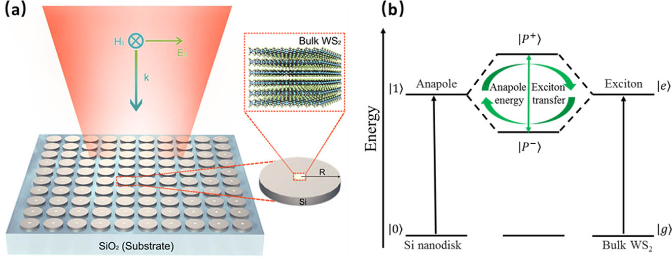
Figure 1.(a) Schematic illustration of the Si nanodisk-bulk
The coupling between anapole modes in the Si nanodisk array and excitons in the bulk can be understood using a simple physical model shown in Fig. 1(b). Generally, when planar incident light impinges on the structure, the ED moment is illustrated as a separation of positive and negative electrical charges, and the TD moment corresponds to currents flowing on the surface of a torus in the Si nanodisk array. Then the destructive interference between the enhanced TD resonance and the ED resonance happens while they have same amplitude but opposite phase, and consequently, the anapole state in the electromagnetic spectrum is realized. The unexcited state and resonant anapole state of Si nanodisks are noted as and , respectively. At the same time, the filled exciton will undergo a transition from the ground state to the excited state with a resonance energy of 1.9 eV under normal illumination. Generally, changing the radius of the Si nanodisk is an efficient optimization way to achieve the spectral overlap. Therefore, it is found that Si nanodisk-bulk heterostructures in the confined electromagnetic environment can reach the strong coupling regime when the anapole mode in the Si nanodisks overlaps the absorption peak of the bulk exciton by adjusting the radius of the Si nanodisk, enabling new hybrid energy states with upper branches (UB) and lower branches (LB) and coherent exchange of energy between the anapole mode and exciton in a reversible way. The energy exchange between light and matter will be periodical temporally, and when the exciton and anapole resonate, two new resonance frequencies can be observed from the transmittance spectrum [41].
3. RESULTS AND DISCUSSION
First, the optical responses of the Si nanodisk array under normal illumination with different structural parameters are studied. In Fig. 2(a), we plot the transmission contour map with respect to radii of Si nanodisks and wavelength of incident light, where the height of the Si nanodisk is . It is noted that one strong resonance mode (transmission dip) can be clearly seen in Fig. 2(a), which displays a prominent redshift with increasing of the nanodisk radius. We have also calculated a transmission contour map as a function of height of the Si nanodisk, with , as shown in Fig. 2(b), and one transmission minimum in the spectra is also found, which only displays a slight redshift with increasing of the height of the Si nanodisk. Considering the position of the bulk exciton peak, we choose the Si nanodisk with a radius of 130 nm and a height of 70 nm, of which the resonance position is labeled as D1. In Fig. 2(c), we show the transmission spectrum of a Si nanodisk array without holes (blue solid curve), a Si nanodisk array with holes (red solid curve), and a Si nanodisk array with bulk () inside holes (black solid curve), with , , and . It is found that the D1 mode of the Si nanodisk array with nanoholes shows a more pronounced blueshift than that of the Si nanodisk array since the refractive index of air is significantly smaller than that of silicon, and the transmission spectrum of the Si nanodisk-bulk () heterostructure array remains almost unchanged compared to that of the Si nanodisk array due to their similar refractive index (see Fig. 5 in Appendix A). From Figs. 2(a)–2(c), it can be summarized that the spectroscopic behavior of D1 mode can be changed by varying structural parameters.
![]()
Figure 2.Analyses of the nonradiating anapole mode in the heterostructures. (a) Simulated transmission contour map as a function of radius of the Si nanodisk array (
In Figs. 2(d)–2(f), we calculate near-field distributions and displacement vector maps under D1 mode. It is found that the displacement vector at the center cross section of the plane forms two circles of opposite directions, which in turn generates a highly curved magnetic field and results in a state whose energy is confined inside the nanodisk, which closely matches those of anapole states from previous works [27,34,42–44]. More importantly, the maximum electric field of these systems is concentrated in the middle of the nanodisk, and the introduction of nanoholes and bulk can result in more enhancement inside the structure than that of the Si nanodisk array as shown in Figs. 2(e) and 2(f). Consequently, the Si nanodisk-bulk heterostructure array is chosen in this coupling study due to the larger electric field enhancement in the position of the bulk .
In addition, to reveal the effect of the periodicity on the D1 mode, optical properties for the different numbers of unit cells of the ()-Si nanodisk heterostructure are also explored with , , and . In Fig. 6(a) (in Appendix B), we plot the scattering intensity of the isolated, -unit cell and -unit cell for the ()-Si nanodisk heterostructure, and it is noted that the lowest total scattering spectrum is located at about 650 nm, and the full width at half-maximum (FWHM) decreases significantly with the increase of the number of the unit cell. Figures 6(b)–6(e) show the -plane electric field distributions at the resonance wavelength, which all have characteristic features of an anapole state. It is found that the FWHM of D1 mode of the heterostructure array decreases significantly, and the electromagnetic enhancement of the heterostructure array is improved considerably compared to that of the isolated heterostructure. Therefore, the periodicity of the structure can boost the near-field properties of the D1 mode. In Fig. 7 (in Appendix B), we plot the transmission spectrum and the near-field distribution of the ()-Si nanodisk heterostructure array with different periodicity size. It is noted that the transmission dip displays a prominent redshift with increasing of the periodicity. Moreover, the heterostructure array with a periodicity of 500 nm exhibits maximum electromagnetic field enhancement inside the bulk , and its resonance wavelength of D1 mode is located near the position of the exciton absorption peak. Therefore, the periodicity of 500 nm is selected in the main text.
![]()
Figure 3.(a) Normalized Cartesian multipole decomposition results for the Si nanodisk-bulk
![]()
Figure 4.Analyses of the resonance coupling in the heterostructures, where the excitonic effect of bulk
To investigate the physical origin of the D1 mode, we calculate the scattered power of ED, magnetic dipole (MD), and TD moments of the heterostructure array with , utilizing the Cartesian multipole decomposition based on the induced current density. In this procedure, the oscillating charge current distribution inside the nanostructure, induced by an incident linearly polarized plane wave, is expanded into a series of electric, magnetic, and toroidal multipole moments. The Cartesian ED (P), MD (M), and TD (T) moments are performed by the following formula in the long-wavelength approximation [45]:
It can be found that the scattered power of ED and TD intersects at about 656 nm, as shown in Fig. 3(a), while the phase difference between them equals approximately , in Fig. 3(b), indicating that the anapole mode is located at 656 nm. From Fig. 8 (in Appendix C), we can see that the transmission dip (D1) has a certain redshift compared to the intersection position of the ED and TD due to the array effect [49–52]. Therefore, strictly speaking, the anapole mode should be located at 656 nm of the transmission spectrum, but since the near-field distribution of D1 mode still satisfies the characteristics of the anapole mode, the D1 mode can be referred to as the weak anapole mode synergetic with the array effect (see Appendix C).
The realization of strong coupling requires the simultaneous spatial and spectral overlap, where the spatial coincidence has been accomplished by putting the bulk into the maximum near-field region of the weak anapole mode in the Si nanodisk array. The spectral coincidence can be achieved by continuously redshifting the optical resonance mode across the excitonic transition by adjusting the radius of the Si nanodisk. In Fig. 9 of Appendix D, we first plot the transmission contour map of the Si nanodisk-bulk () heterostructure array with respect to the radii of the Si nanodisks and wavelength of incident light. It is found that the optical resonance mode redshifts from 580 to 825 nm as radius of the Si nanodisk increases from 100 to 200 nm. Therefore, changing the radius of the Si nanodisk is an efficient way to achieve the spectral overlap between the optical resonance mode and exciton. In Fig. 4(a), we present the simulated radius-dependent transmission spectra of the hybrid nanostructure array with , , and . It is noted that clear evidence of strong coupling spectral splitting is manifested in the transmission spectra as the weak anapole resonance energy shifts across the exciton. In order to obtain the coupling strength, we extract two dips of multiple transmission spectra in Fig. 4(a), as marked in Fig. 4(b) (blue and red spheres), and we use the classic coupled oscillator model to provide an accurate physical analyzer to reveal coupling behaviors in the hybrid nanostructure. In this model, the response of excitons can be viewed as an oscillator, and then the system can be modeled as two coupled harmonic oscillators:
Next, the resonance coupling for the heterostructure system with different radius r of is demonstrated in Appendix E. For , the weak anapole mode in the transmission spectra displays a weak redshift with increasing r as shown in Fig. 10(a) (in Appendix E). For , we can see that the splitting between the LB and UB hybrid modes is broadening with the increase of r [see Fig. 10(b) in Appendix E]. When r is in the range from 60 to 100 nm, the middle transmission dip is attributed to the Mie resonance mode of bulk due to its high refractive index. This observation can be understood by investigating the electromagnetic field enhancement of the heterostructure array with different radius of 20, 50, and 100 nm, respectively, which is shown in Figs. 10(c)–10(e) (in Appendix E). It is found that the electromagnetic field enhancement inside the bulk is much larger for than for the other two. Moreover, a Rabi splitting of 260 meV can be acquired with from Fig. 10, which is far greater than the previous work [33], revealing that the heterostructure array can enhance the interaction between bulk excitons and the anapole mode compared with a single nanodisk. In Fig. 11 (in Appendix E), we plot the transmission contour map with respect to oscillator strength and wavelength of incident light for the heterostructure array. It is found that the splitting between the LB and UB hybrid anapole modes is broadening with the increasing of . The refractive index is proportional to , and a stronger dipole moment would be generated for the bulk with a larger [34]. Therefore, a stronger polarized electromagnetic field generated by bulk can be felt by the Si nanodisk when is enlarged, which will lead to a stronger resonance coupling between the exciton and the anapole mode.
In Appendix F, the coupling behavior is studied when the bulk is put outside the Si nanodisk. There exists no dip splitting in the transmission spectra while the is placed on top of the Si nanodisk surface as shown in Fig. 12(a) (in Appendix F). A strong coupling regime with a smaller Rabi splitting can be achieved when the is put on the side of the Si nanodisk as shown in Fig. 12(b) (in Appendix F). We can reasonably deduce that the very weak coupling strength between excitons and anapole modes is due to the fact that electromagnetic field enhancement caused by the weak anapole mode is away from the . Moreover, in Fig. 13 (in Appendix G), we studied the coupling characteristic of the Si nanodisk-J-Aggregate heterostructure array, where the radii of the J-Aggregate and the Si nanodisk are 40 nm and 150 nm, respectively. We found that the anapole mode supported by perforated Si nanodisks can be strongly coupled to the J-Aggregate with a Rabi splitting of 200 meV, which is far greater than in previous works [34]. It is noted that the Rabi splitting in our strategy can be largely amplified, compared with systems where the J-Aggregates are placed outside the Si nanodisk directly.
4. CONCLUSIONS
In summary, we have studied the coupling characteristics of excitons and anapole modes in a Si nanodisk-bulk heterostructure array using FDTD. By opening up a dedicated nanohole at the center of the Si nanodisk, the inside electrical field generated by the anapole modes reaches its maximum, i.e., the near-field enhancement can be significantly amplified. At the same time, the nanohole structure makes it feasible to realize spatial overlap between excitons in bulk and the confined electromagnetic energy. Strong coupling with a large Rabi splitting of 151 meV is obtained. The present work may provide theoretical contributions to potential applications in optoelectronic devices, light harvesting, and photocatalysis.
Acknowledgment
Acknowledgment. The authors thank Dr. Shaoxin Shen and Dr. Yan Chen for helpful discussions.
APPENDIX A: REFRACTIVE INDEX OF BULK WS2
To compare the refractive index of the Si and bulk WS2, we give the specific refractive index of bulk WS2 including the case of = 0 and = 0.4 in Fig.
![]()
Figure 5.Wavelength dependence of the (a), (b) real and (c), (d) imaginary parts of the in-plane complex index of refraction for a Lorentz model dielectric of bulk
APPENDIX B: ADVANTAGES OF THE PERIODICITY
In Fig.
![]()
Figure 6.(a) Simulated scattering spectrum of isolated,
![]()
Figure 7.(a) Simulated transmission spectrum for Si nanodisk-bulk
APPENDIX C: MULTIPOLES AND TOTAL SCATTERING POWER
In Fig.
![]()
Figure 8.(a) Normalized corresponding transmission spectra and contributions from different multipoles for the Si nanodisk-bulk
APPENDIX D: RADIUS-DEPENDENT TRANSMISSION SPECTRA
In Fig.
![]()
Figure 9.Simulated transmission contour map as a function of radius of the Si nanodisk (
APPENDIX E: RADIUS-DEPENDENT AND f-DEPENDENT OF THE WS2 TRANSMISSION SPECTRA AND NEAR-FIELD DISTRIBUTION
In Fig.
![]()
Figure 10.(a) Simulated transmission contour map as a function of radius of the
![]()
Figure 11.(a) Simulated transmission contour map as a function of
APPENDIX F: RADIUS-DEPENDENT TRANSMISSION SPECTRA OF DIFFERENT POSITIONS OF WS2
In Fig.
![]()
Figure 12.(a) Simulated transmission contour map as a function of radius of the Si nanodisk (
APPENDIX G: TRANSMISSION SPECTRA OF THE Si NANODISK-J-AGGREGATE HETEROSTRUCTURE ARRAY
In Fig.
![]()
Figure 13.(a) Simulated transmission spectrum of the Si nanodisk array, where the radius of the Si nanodisk is
References
[1] C. Li, S. Duan, B. Wen, S. B. Li, M. Kathiresan, L. Q. Xie, S. Chen, J. R. Anema, B. W. Mao, Y. Luo, Z. Q. Tian, J. F. Li. Observation of inhomogeneous plasmonic field distribution in a nanocavity. Nat. Nanotechnol., 15, 922-926(2020).
[2] Y. He, W. Yang, T. M. Shih, J. Wang, D. Zhang, M. Gao, F. Jiao, Y. Zeng, J. L. Yang, J. Pang, R. Gao, G. Sun, M. D. Li, J. F. Li, Z. Yang. Manipulation of ultrafast nonlinear optical response based on surface plasmon resonance. Adv. Opt. Mater., 9, 2100847(2021).
[3] J. Park, S. Hong, Y. S. Lee, H. Lee, S. Kim, K. Dholakia, K. Oh. Optical manipulation of a dielectric particle along polygonal closed-loop geometries within a single water droplet. Sci. Rep., 11, 12690(2021).
[4] W.-J. Chen, M. Xiao, C. T. Chan. Photonic crystals possessing multiple Weyl points and the experimental observation of robust surface states. Nat. Commun., 7, 13038(2016).
[5] S. Yu, C.-W. Qiu, Y. Chong, S. Torquato, N. Park. Engineered disorder in photonics. Nat. Rev. Mater., 6, 226-243(2021).
[6] D. Brunner, M. C. Soriano, C. R. Mirasso, I. Fischer. Parallel photonic information processing at gigabyte per second data rates using transient states. Nat. Commun., 4, 1364(2013).
[7] S. H. Huang, X. Jiang, B. Peng, C. Janisch, A. Cocking, Ş. K. Özdemir, Z. Liu, L. Yang. Surface-enhanced Raman scattering on dielectric microspheres with whispering gallery mode resonance. Photon. Res., 6, 346-356(2018).
[8] Z. Shen, Y.-L. Zhang, C.-L. Zou, G.-C. Guo, C.-H. Dong. Dissipatively controlled optomechanical interaction via cascaded photon-phonon coupling. Phys. Rev. Lett., 126, 163604(2021).
[9] N. Muhammad, Y. Chen, C. W. Qiu, G. P. Wang. Optical bound states in continuum in MoS2-based metasurface for directional light emission. Nano Lett., 21, 967-972(2021).
[10] J. J. Baumberg, J. Aizpurua, M. H. Mikkelsen, D. R. Smith. Extreme nanophotonics from ultrathin metallic gaps. Nat. Mater., 18, 668-678(2019).
[11] L. Sun, Z. Li, J. He, P. Wang. Strong coupling with directional absorption features of Ag@Au hollow nanoshell/J-aggregate heterostructures. Nanophotonics, 8, 1835-1845(2019).
[12] J. Sun, H. Hu, D. Zheng, D. X. Zhang, Q. Deng, S. P. Zhang, H. X. Xu. Light-emitting plexciton: exploiting plasmon-exciton interaction in the intermediate coupling regime. ACS Nano, 12, 10393-10402(2018).
[13] H. Shan, Y. Yu, X. L. Wang, Y. Luo, S. Zu, B. W. Du, T. Y. Han, B. W. Li, Y. Li, J. R. Wu, F. Lin, K. B. Shi, B. K. Tay, Z. Liu, X. Zhu, Z. Y. Fang. Direct observation of ultrafast plasmonic hot electron transfer in the strong coupling regime. Light Sci. Appl., 8, 9(2019).
[14] J. Wang, W. Lin, X. Xu, F. Ma, M. Sun. Plasmon-exciton coupling interaction for surface catalytic reactions. Chem. Rec., 18, 481-490(2018).
[15] J. Wang, W. Yang, P. M. Radjenovic, Y. He, Z. Yang, J. F. Li. Strong coupling between magnetic resonance and propagating surface plasmons at visible light frequencies. J. Chem. Phys., 152, 014702(2020).
[16] T. Qu, F. Liu, Y. Lin, K. Cui, X. Feng, W. Zhang, Y. Huang. Cherenkov radiation generated in hexagonal boron nitride using extremely low-energy electrons. Nanophotonics, 9, 1491-1499(2020).
[17] L. Meng, R. Yu, M. Qiu, F. J. García de Abajo. Plasmonic nano-oven by concatenation of multishell photothermal enhancement. ACS Nano, 11, 7915-7924(2017).
[18] M. Moskovits. Surface-enhanced spectroscopy. Rev. Mod. Phys., 57, 783-826(1985).
[19] S. A. Maier, H. A. Atwater. Plasmonics: localization and guiding of electromagnetic energy in metal/dielectric structures. J. Appl. Phys., 98, 011101(2005).
[20] H. Wang, Y. Ke, N. Xu, R. Zhan, Z. Zheng, J. Wen, J. Yan, P. Liu, J. Chen, J. She, Y. Zhang, F. Liu, H. Chen, S. Deng. Resonance coupling in silicon nanosphere-J-aggregate heterostructures. Nano Lett., 16, 6886-6895(2016).
[21] M. V. Rybin, K. L. Koshelev, Z. F. Sadrieva, K. B. Samusev, A. A. Bogdanov, M. F. Limonov, Y. S. Kivshar. High-
[22] O. Yavas, M. Svedendahl, R. Quidant. Unravelling the role of electric and magnetic dipoles in biosensing with Si nanoresonators. ACS Nano, 13, 4582-4588(2019).
[23] A. I. Kuznetsov, A. E. Miroshnichenko, M. L. Brongersma, Y. S. Kivshar, B. Luk’yanchuk. Optically resonant dielectric nanostructures. Science, 354, aag2472(2016).
[24] K. Koshelev, G. Favraud, A. Bogdanov, Y. Kivshar, A. Fratalocchi. Nonradiating photonics with resonant dielectric nanostructures. Nanophotonics, 8, 725-745(2019).
[25] G.-M. Pan, F.-Z. Shu, L. Wang, L. Shi, A. B. Evlyukhin. Plasmonic anapole states of active metamolecules. Photon. Res., 9, 822-828(2021).
[26] X. Li, J. Yin, J. Liu, F. Shu, T. Lang, X. Jing, Z. Hong. Resonant transparency of a planar anapole metamaterial at terahertz frequencies. Photon. Res., 9, 125-130(2021).
[27] A. E. Miroshnichenko, A. B. Evlyukhin, Y. F. Yu, R. M. Bakker, A. Chipouline, A. I. Kuznetsov, B. Luk’yanchuk, B. N. Chichkov, Y. S. Kivshar. Nonradiating anapole modes in dielectric nanoparticles. Nat. Commun., 6, 8069(2015).
[28] Y. Yang, V. A. Zenin, S. I. Bozhevolnyi. Anapole-assisted strong field enhancement in individual all-dielectric nanostructures. ACS Photon., 5, 1960-1966(2018).
[29] J. S. Totero Gongora, A. E. Miroshnichenko, Y. S. Kivshar, A. Fratalocchi. Anapole nanolasers for mode-locking and ultrafast pulse generation. Nat. Commun., 8, 15535(2017).
[30] D. G. Baranov, R. Verre, P. Karpinski, M. Käll. Anapole-enhanced intrinsic Raman scattering from silicon nanodisks. ACS Photon., 5, 2730-2736(2018).
[31] G. Grinblat, Y. Li, M. P. Nielsen, R. F. Oulton, S. A. Maier. Enhanced third harmonic generation in single germanium nanodisks excited at the anapole mode. Nano Lett., 16, 4635-4640(2016).
[32] J. J. Hernandez-Sarria, O. N. Oliveira, J. R. Mejia-Salazar. Toward lossless infrared optical trapping of small nanoparticles using nonradiative anapole modes. Phys. Rev. Lett., 127, 186803(2021).
[33] R. Verre, D. G. Baranov, B. Munkhbat, J. Cuadra, M. Kall, T. Shegai. Transition metal dichalcogenide nanodisks as high-index dielectric Mie nanoresonators. Nat. Nanotechnol., 14, 679-683(2019).
[34] S.-D. Liu, J.-L. Fan, W.-J. Wang, J.-D. Chen, Z.-H. Chen. Resonance coupling between molecular excitons and nonradiating anapole modes in silicon nanodisk-J-aggregate heterostructures. ACS Photon., 5, 1628-1639(2018).
[35] K. As’ham, I. Al-Ani, L. Huang, A. E. Miroshnichenko, H. T. Hattori. Boosting strong coupling in a hybrid WSe2 monolayer–anapole–plasmon system. ACS Photon., 8, 489-496(2021).
[36] K. Du, P. Li, K. Gao, H. Wang, Z. Yang, W. Zhang, F. Xiao, S. J. Chua, T. Mei. Strong coupling between dark plasmon and anapole modes. J. Phys. Chem. Lett., 10, 4699-4705(2019).
[37] K. V. Baryshnikova, D. A. Smirnova, B. S. Luk’yanchuk, Y. S. Kivshar. Optical anapoles: concepts and applications. Adv. Opt. Mater., 7, 1801350(2019).
[38] Z. Fenghua, C. Zhizhang, Z. Jiazong. Toward the development of a three-dimensional unconditionally stable finite-difference time-domain method. IEEE Trans. Microw. Theory, 48, 1550-1558(2000).
[39] E. D. Palik. Handbook of Optical Constants of Solids(1998).
[40] S. Wang, Q. Le-Van, F. Vaianella, B. Maes, S. Eizagirre Barker, R. H. Godiksen, A. G. Curto, J. G. Rivas. Limits to strong coupling of excitons in multilayer WS2 with collective plasmonic resonances. ACS Photon., 6, 286-293(2019).
[41] E. Cao, W. H. Lin, M. T. Sun, W. J. Liang, Y. Z. Song. Exciton-plasmon coupling interactions: from principle to applications. Nanophotonics, 7, 145-167(2018).
[42] B. Luk’yanchuk, R. Paniagua-Domínguez, A. I. Kuznetsov, A. E. Miroshnichenko, Y. S. Kivshar. Hybrid anapole modes of high-index dielectric nanoparticles. Phys. Rev. A, 95, 063820(2017).
[43] S.-Q. Li, K. B. Crozier. Origin of the anapole condition as revealed by a simple expansion beyond the toroidal multipole. Phys. Rev. B, 97, 245423(2018).
[44] E. A. Gurvitz, K. S. Ladutenko, P. A. Dergachev, A. B. Evlyukhin, A. E. Miroshnichenko, A. S. Shalin. The high-order toroidal moments and anapole states in all-dielectric photonics. Laser Photon. Rev., 13, 1800266(2019).
[45] E. E. Radescu, G. Vaman. Exact calculation of the angular momentum loss, recoil force, and radiation intensity for an arbitrary source in terms of electric, magnetic, and toroid multipoles. Phys. Rev. E, 65, 046609(2002).
[46] R. Wang, L. Dal Negro. Engineering non-radiative anapole modes for broadband absorption enhancement of light. Opt. Express, 24, 19048-19062(2016).
[47] C. Zhou, S. Li, M. Fan, X. Wang, Y. Xu, W. Xu, S. Xiao, M. Hu, J. Liu. Optical radiation manipulation of Si-Ge2Sb2Te5 hybrid metasurfaces. Opt. Express, 28, 9690-9701(2020).
[48] S. Li, C. Zhou, T. Liu, S. Xiao. Symmetry-protected bound states in the continuum supported by all-dielectric metasurfaces. Phys. Rev. A, 100, 063803(2019).
[49] P. C. Wu, C. Y. Liao, V. Savinov, T. L. Chung, W. T. Chen, Y. W. Huang, P. R. Wu, Y. H. Chen, A. Q. Liu, N. I. Zheludev, D. P. Tsai. Optical anapole metamaterial. ACS Nano, 12, 1920-1927(2018).
[50] V. A. Fedotov, N. Papasimakis, E. Plum, A. Bitzer, M. Walther, P. Kuo, D. P. Tsai, N. I. Zheludev. Spectral collapse in ensembles of metamolecules. Phys. Rev. Lett., 104, 223901(2010).
[51] S. Campione, S. Liu, L. I. Basilio, L. K. Warne, W. L. Langston, T. S. Luk, J. R. Wendt, J. L. Reno, G. A. Keeler, I. Brener, M. B. Sinclair. Broken symmetry dielectric resonators for high quality factor Fano metasurfaces. ACS Photon., 3, 2362-2367(2016).
[52] A. V. Kuznetsov, A. C. Valero, M. Tarkhov, V. Bobrovs, D. Redka, A. S. Shalin. Transparent hybrid anapole metasurfaces with negligible electromagnetic coupling for phase engineering. Nanophotonics, 10, 4385-4398(2021).

Set citation alerts for the article
Please enter your email address
© Copyright 2018-2021 | Chinese Laser Press. All Rights Reserved 沪ICP备15018463号-20