• Photonics Research
  • Vol. 10, Issue 7, 1731 (2022)
Shoujun Zhang1, Xieyu Chen1, Kuan Liu2, Haiyang Li2, Yuehong Xu1, Xiaohan Jiang1, Yihan Xu1, Qingwei Wang1, Tun Cao2、4、*, and Zhen Tian1、3、5、*
Author Affiliations
  • 1Center for Terahertz Waves and College of Precision Instrument and Optoelectronics Engineering, Key Laboratory of Optoelectronic Information Technology (Ministry of Education of China), Tianjin University, Tianjin 300072, China
  • 2School of Optoelectronic Engineering and Instrumentation Science, Dalian University of Technology, Dalian 116024, China
  • 3Georgia Tech Shenzhen Institute (GTSI), Tianjin University, Shenzhen 518067, China
  • 4e-mail: caotun1806@dlut.edu.cn
  • 5e-mail: tianzhen@tju.edu.cn
  • show less
    DOI: 10.1364/PRJ.456161 Cite this Article Set citation alerts
    Shoujun Zhang, Xieyu Chen, Kuan Liu, Haiyang Li, Yuehong Xu, Xiaohan Jiang, Yihan Xu, Qingwei Wang, Tun Cao, Zhen Tian. Nonvolatile reconfigurable dynamic Janus metasurfaces in the terahertz regime[J]. Photonics Research, 2022, 10(7): 1731 Copy Citation Text show less

    Abstract

    Metasurfaces, especially tunable ones, have played a major role in controlling the amplitude, phase, and polarization of electromagnetic waves and attracted growing interest, with a view toward a new generation of miniaturized devices. However, to date, most existing reconfigurable devices are bounded in volatile nature with sustained external energy to maintain and single functionality, which restrict their further applications. Here, we demonstrate for the first time, to our knowledge, nonvolatile, reconfigurable, and dynamic Janus metasurfaces by incorporating phase-change material Ge2Se2Te5 (GST) in the terahertz (THz) regime. First, we experimentally show the reversible switching characteristic of GST on large areas by applying a single nanosecond laser pulse, which exhibits excellent contrast of THz properties in both states. Then, we present a multiplex metasurface scheme. In each metasurface, three sets of structures are adopted, in which two sets integrate GST. The effective structures can be reversely modulated by the amorphization and crystallization of GST. As a proof of concept, the dynamic beam splitter, bifocal metalens, dual-mode focusing optical vortex generators, and switchable metalens/focusing optical vortex generators are designed, fabricated, and experimentally characterized, and can be switched reversibly and repeatedly with the help of optical and thermal stimuli. Our scheme will pave the way toward the development of multifunctional and compact THz devices and may find use for applications in THz imaging, sensing, and communications.

    1. INTRODUCTION

    Metasurfaces, as 2D metamaterials consisting of an array of function-driven artificial meta-atoms, have attracted tremendous attention due to their unprecedented abilities in manipulating the phase, polarization, and amplitude of electromagnetic (EM) waves [1]. In the terahertz (THz) frequency band, metasurfaces have resulted in numerous applications, including absorbers [2], metalenses [3], beam steering [4], holography [5,6], vector beams [7], topological waveguides [8], bound states in the continuum [9,10], etc. Despite metasurfaces having exhibited clear advantages over classical optical components, their performances are fixed upon fabrication, which limits their further applications. So actively tuning the properties of EM waves is highly desirable for integrated photonic systems [11,12]. Currently, various active modulation methods have been proposed, such as liquid crystals (LCs) [1315], semiconductors [1618], microelectromechanical system (MEMS) [1921], graphene [2224], and phase-change material (PCM) [2529]. These mechanisms of active modulation have led to a diverse range of tunable THz metasurfaces [13,16,17,20,2224,2629]. However, a constant stimulus is needed to preserve the working states of devices, and there has yet to be developed an energy-efficient solution for maintaining the desired function with zero static power consumption in the THz regime. Moreover, most of these approaches are limited to a single functionality, which hinders their further applications.

    Ge2Se2Te5 (GST), as one of the most popular chalcogenide PCMs, has been widely used in the field of data storage due to its unique phase-change characteristics [30,31]. It exhibits dramatic differences in optical properties between its amorphous and crystalline states and can be repeatedly switched between these states through thermal, electrical, and optical stimuli. Crystallization of GST can be induced by applying long and relatively moderate-intensity pulses (optical or electrical) to locally heat amorphous GST (A-GST) to its crystallization temperature or by heating the whole sample up (i.e., thermal) and holding for a short time. By contrast, amorphization can be achieved by applying high-intensity pulses with a short duration to heat crystalline GST (C-GST) above the melting point and then rapidly quenching it to prevent any recrystallization [32]. Once the crystallization or reamorphization has been realized, the state of GST is stable for years with zero hold power at room temperature (compared with another PCM, VO2, which is volatile) [31,33]. In view of these excellent properties, GST has been used in the development of integrated all-optical memory devices [3436], photonic neuromorphic devices [3739], color displays [40], thermal emitters [41], and plasmonic and dielectric metasurfaces [42,43] in the visible and infrared domains. In addition, Janus metasurfaces, inspired by the two-faced god Janus in Roman mythology, have shown tremendous potential in controlling EM waves by integrating different functionalities in a single structural layer [4447]. However, in the THz regime, researches on the reversible phase transition in large-scale areas and applications of GST are still under exploration [2729], and nonvolatile dynamic Janus metasurfaces that can realize switchable functions in both states of GST have not been reported.

    In this work, we demonstrate a novel class of nonvolatile, reconfigurable, and dynamic Janus metasurfaces by incorporating PCM GST in the THz regime, which can offer a wealth of switchable functionalities. The metasurfaces comprise three sets of functional structures arranged using multiplex methods: two active sets composed of GST integrated C-shaped slit resonators (G-CRs) and a passive set composed of CRs. In the amorphous state of GST, the function of the device depends on the contribution of three sets of structures; however, the function is governed by the passive set in the crystalline state. Here, we experimentally show the reversible switching characteristic of GST on large areas by applying a single ns-laser pulse with a diameter of 1 cm to achieve amorphization of GST and heating the entire sample on a hot plate to induce crystallization. Based on this scheme, several important bifunctional metasurfaces are designed, fabricated, and experimentally characterized, including dynamic beam splitter, bifocal metalens, dual-mode focusing optical vortex (FOV) generators, and switchable metalens/FOV generators. Experimental results show that the proposed metasurfaces can realize two independent functionalities in both states and can be switched reversibly and repeatedly. Moreover, the function in a certain phase is stable with zero hold power at room temperature. The proposed nonvolatile, reconfigurable, and dynamic Janus metasurfaces combined with GST provide a novel way to realize multifunctional and compact THz devices and may have essential applications in THz integrated devices, imaging, and communications.

    2. RESULTS

    A. Design Principles

    A schematic diagram of the proposed nonvolatile, reconfigurable Janus metasurface is shown in Fig. 1(a), which demonstrates the reversible switching between the mth-order FOV and metalens. To realize the modulation of phase and amplitude of transmitted THz waves, we select the Babinet-inverted, complementary C-shaped split-ring resonators–CRs as basic meta-atoms due to their strong response to THz radiation [25]. The geometrical parameters of CRs are schematically illustrated in Fig. 1(b). Px=Py=80  μm is the period, r is the outer ring radius, w is the line width, α is the opening angle, and β is the orientation angle. By changing the geometrical parameters of CRs, the amplitude and phase of cross-polarization can be simultaneously controlled. To enable an abrupt phase shift covering a 2π range and a nearly constant transmission amplitude, numerical simulations are carried out to select resonators by tuning w, r, and α of CRs using commercial software computer simulation technology (CST) Microwave Studio. The CRs are made of a 200-nm-thick aluminum (Al) film on a 2-mm-thick silicon (Si) substrate, and the β are fixed at ±45°. A normally incident plane wave with y polarization is used to excite the structure, and scattered cross-polarization is detected. Eight CRs with nearly the same transmission amplitude and a π/4 phase-change interval are selected at 0.8 THz, as shown in Fig. 1(c). To realize the proposed nonvolatile, reconfigurable Janus metasurface, we incorporate GST, which exhibits a drastic contrast in THz transmission between amorphous and crystalline states and good repeatability (see Appendix A for more details).

    Operation principle of dynamic Janus metasurface. (a) Schematic demonstration of a nonvolatile reconfigurable Janus metasurface consisting of three sets of structures, U1, U2, and U3. Green, lilac, and gray structures are metallic CRs, amorphous G-CRs, and crystalline G-CRs, respectively. Incident THz waves are y-polarization, and cross-polarization transmitted waves are detected. Any two functionalities can be switched reversibly by recrystallization and reamorphization. Inset shows enlarged views of U1, U2, and U3. In active structures U1 and U2, there is an additional layer of GST between the Al CRs and the silicon substrate. (b) Schematic view of a single CR: Px=Py=80 μm is the period, r is the outer ring radius, w is the line width, α is the opening angle, and β is the orientation angle. (c) Simulated amplitude and phase shift of eight CRs at 0.8 THz. Geometrical parameters of the former four CRs are r=37,37,38,38 μm, w=8,15,9,5 μm, and α=120°,40°,30°,12°, respectively, with the same rotation angle β=45°. Another four structures can be obtained by mirroring along the y axis.

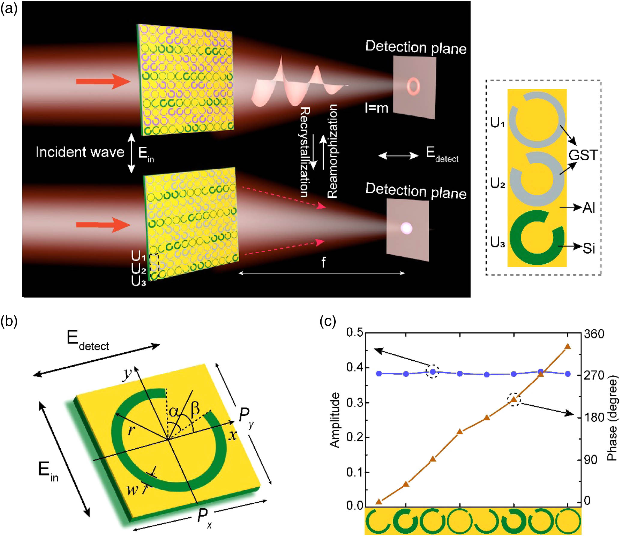
    Figure 1.Operation principle of dynamic Janus metasurface. (a) Schematic demonstration of a nonvolatile reconfigurable Janus metasurface consisting of three sets of structures, U1, U2, and U3. Green, lilac, and gray structures are metallic CRs, amorphous G-CRs, and crystalline G-CRs, respectively. Incident THz waves are y-polarization, and cross-polarization transmitted waves are detected. Any two functionalities can be switched reversibly by recrystallization and reamorphization. Inset shows enlarged views of U1, U2, and U3. In active structures U1 and U2, there is an additional layer of GST between the Al CRs and the silicon substrate. (b) Schematic view of a single CR: Px=Py=80  μm is the period, r is the outer ring radius, w is the line width, α is the opening angle, and β is the orientation angle. (c) Simulated amplitude and phase shift of eight CRs at 0.8 THz. Geometrical parameters of the former four CRs are r=37,37,38,38  μm, w=8,15,9,5  μm, and α=120°,40°,30°,12°, respectively, with the same rotation angle β=45°. Another four structures can be obtained by mirroring along the y axis.

    The working principle is presented in Fig. 1(a). The metasurface consists of three sets of functional structures arranged using multiplex methods, as shown in the black rectangular box: two active sets (U1 and U2) composed of G-CRs, which can be reversibly switched between amorphous and crystalline states by optical and thermal stimuli, and a passive set (U3) composed of CRs, which exhibits a fixed response. The inset shows enlarged views of U1, U2, and U3. In active structures U1 and U2, there is an additional layer of GST between the Al CRs and the Si substrate. In the amorphous state of GST, we enable the far-field diffraction patterns of U2 and U3 to exhibit nearly constant amplitude and phase delay of π in the detection plane. The effective structures are U1 due to destructive interference. However, in the crystalline state of GST, the transmission amplitudes of G-CRs nearly approach zero (see Appendix B for more details); thus, the effective structures are U3. In other words, in the amorphous state of GST, the metasurface functionality is determined by the effective set U1; after crystallization, the amorphous G-CRs transition into crystalline G-CRs, and the function of the multiplex structures is governed by the passive set U3. By reamorphization, the function can be switched back. Here, we apply 1064-nm wavelength nanosecond laser pulses to reamorphize GST and heat the entire sample on a hot plate to induce crystallization. The following explains why the heating procedure is chosen over the short laser pulse irradiation process. When A-GST is heated to about 300°C, it transforms into a hexagonal-centered cubic phase (HCP), and when the sample is irradiated with short laser pulses, it transforms into a face-centered cubic phase (FCC) [48,49]; the THz wave transmission change through the sample during the amorphous-to-HCP process is more dramatic than during the amorphous-to-FCC process [28]. It should be noted that our device is nonvolatile without a constant stimulus to maintain (compared with the alternative PCM VO2, which is volatile). Therefore, by designing and arranging three sets of structures properly, any two functionalities can be realized in both states of GST and can be reversibly switched, without changing any optical elements in the optical path during the entire process.

    B. Nonvolatile Dynamic Reversible Switching of Bifunctional Metasurfaces

    First, a dynamic beam splitter is demonstrated using our Janus metasurface, as shown in Fig. 2(a). The anomalous refraction of cross-polarization THz waves propagates along two opposite directions in crystalline and amorphous states of GST at normal incidence of y-polarization THz waves. To experimentally prove the reliability of the designed dynamic beam splitter, we fabricated a metasurface on a 2-mm-thick Si substrate by conventional multistep lithography. The microscope optical image of part of the fabricated sample and enlarged views of basic units comprising three sets of functional structures are shown in Fig. 2(b). The metasurfaces consist of two active sets (U1 and U2) composed of G-CRs and a passive set (U3), which are designed and arranged to obtain the desired phase profiles. The phase distribution of structure set U1 is designed to steer the transmitted waves to the right, whereas U3 is designed to steer beams to the left; U2 is arranged to exhibit a phase delay of π compared to U3, which results in destructive interference. Fiber-based angle-resolved THz time-domain spectroscopy (FAT-TDS) [4,25] is used to characterize the device; y-polarized THz waves are normally incident on the sample from the substrate side, and cross-polarized radiations are detected at different angles from 80° to 80° with a 1° step. Figure 2(c) shows the measured normalized far-field intensity distributions as a function of the deflection angle and frequency. Nearly all output waves are steered to the left around the broadband frequency range from 0.5 to 0.9 THz in the crystalline state of GST, whereas, after applying a single 120  mJ/cm2 laser pulse with 1064 nm wavelength, 7 ns pulse width, and 1 cm spot diameter, the deflected beam is steered to the right and also exhibits a broadband feature. Figure 2(d) shows the corresponding normalized intensity profiles at 0.8 THz extracted from Fig. 2(c). The deflection angles are 36° and 37°, respectively, in both states, which agree well with the theoretically calculated values by the generalized Snell’s law θ=±arcsin[λ/(8P)]=±35.87°, where λ is the wavelength, and P is the period. To further demonstrate the repeatability of the designed Janus device, another switching cycle is performed, and the normalized intensity distributions and corresponding profiles at 0.8 THz are shown in Figs. 2(e) and 2(f), respectively. Here, recrystallization of GST is realized by thermally annealing the sample at 300°C for 2 min on a hot plate. In both states, the deflection angles are 35° and 36°, respectively. The slight deviation in results between the two cycles is primarily due to system measurement. Figure 2(g) shows the calculated and measured dependence of the deflection angle on frequency. The results reveal that the measured dispersive components deflected at different angles obey the generalized Snell’s law, which also validates the measured results. Except for a slight deviation at lower frequencies, due primarily to the large deflection angle and low signal strength, the experimental results are in good agreement with the theoretical calculations. The beam splitting ratios are calculated, which show a broadband feature in both states of GST and are switched from 6.91 to 6.3  dB at 0.7 THz for the crystalline and amorphous states, respectively (see Appendix D for more details).

    Dynamic beam steering. (a) Schematic principle of the proposed dynamic beam splitter, which can steer cross-polarization THz waves toward two opposite directions in crystalline and amorphous states. (b) Optical microscope image of part of the fabricated metasurface and enlarged views of basic elements. The sample is composed of three sets of structures: U1, U2, and U3. The area of the fabricated metasurface is 5120 μm×5120 μm. (c), (e) Measured normalized intensity distribution as a function of deflection angle and frequency. By applying a single pulse with 120 mJ/cm2, the GST is transited from crystalline to amorphous state, and recrystallization of GST is realized by thermally annealing the sample at 300°C for 2 min on a hot plate. (d), (f) Corresponding normalized intensity profiles at 0.8 THz extracted from (c) and (e). (g) Experimentally measured and theoretically calculated deflection angles at various frequencies.

    Figure 2.Dynamic beam steering. (a) Schematic principle of the proposed dynamic beam splitter, which can steer cross-polarization THz waves toward two opposite directions in crystalline and amorphous states. (b) Optical microscope image of part of the fabricated metasurface and enlarged views of basic elements. The sample is composed of three sets of structures: U1, U2, and U3. The area of the fabricated metasurface is 5120  μm×5120  μm. (c), (e) Measured normalized intensity distribution as a function of deflection angle and frequency. By applying a single pulse with 120  mJ/cm2, the GST is transited from crystalline to amorphous state, and recrystallization of GST is realized by thermally annealing the sample at 300°C for 2 min on a hot plate. (d), (f) Corresponding normalized intensity profiles at 0.8 THz extracted from (c) and (e). (g) Experimentally measured and theoretically calculated deflection angles at various frequencies.

    Second, a dynamic bifocal metalens is proposed that exhibits switchable focal lengths in amorphous and crystalline states of GST, as depicted in Fig. 3(a). Structure sets U1 and U3 are designed to obtain the acquired phase profiles for realizing two distinct focal lengths with f1=7  mm and f2=10  mm, respectively, at 0.8 THz. U2 is arranged to exhibit a phase shift of π compared to U3 in the focal plane, which results in destructive interference. The phase profiles are obtained as follows: ϕ11(x,y)=2πλ(x2+y2+f12f1),ϕ12(x,y)=2πλ(x2+y2+f22f2)+π,ϕ13(x,y)=2πλ(x2+y2+f22f2),where λ is the wavelength, and f1 and f2 are the designed focal lengths. For ϕnm, index n is the metasurface functionality number, and m is the sub-surface particle design criteria in Eqs. (1)–(3). To experimentally verify the performance of the device, we fabricate the sample by conventional multistep lithography. The optical microscope image of part of the fabricated sample and enlarged views of three structure sets are shown in Fig. 3(b). Near-field scanning THz microscopy (NSTM) [7] is applied to characterize the device. Y-polarization THz waves normally illuminate on the sample from the side of the substrate and x-polarization THz electric field is detected. Figures 3(c) and 3(d) show the normalized xz and xy plane electric field distributions, respectively, in the amorphous state of GST. By thermal annealing at 300°C for 2 min on a hot plate, GST is switched from the amorphous to crystalline state, and by applying a single 120  mJ/cm2 laser pulse with 1064 nm wavelength, 7 ns pulse width, and 1 cm spot diameter, reamorphization of GST is realized. The measured results are shown in Figs. 3(e)–3(h), respectively. As we can see, in both states of GST, the designed metalenses exhibit different focal lengths, and nearly all of the energy is converged to the focal point. To further characterize the performance of bifocal metalenses, we extract the THz intensity distributions along the propagation direction and the y direction, as illustrated in Figs. 3(i) and 3(j). It can be seen that the measured focal lengths are 6.6 mm, 8.8 mm, and 6.6 mm in amorphous, crystalline, and reamorphization states, respectively, which are smaller than the designed results. This experimental error in focal length is caused by the incident THz beam being slightly focused instead of a perfectly collimated plane wave. The measured full width at half maximum (FWHM) values are around 0.29 μm, 0.37 μm, and 0.27 μm, respectively, which indicates the subwavelength focusing performance. The proposed bifocal metalens exhibits excellent nonvolatile dynamic switchable characteristics in amorphous and crystalline states of GST with the help of optical and thermal stimuli. The calculated amplitude ratios are 14.15 dB and 6  dB at z=6.6  mm and 8.8 mm, respectively (see Appendix D for more details).

    Dynamic bifocal metalens. (a) Schematic principle of the proposed dynamic bifocal metalens, which exhibits switchable focal lengths in amorphous and crystalline states of GST. (b) Optical microscope image of part of the fabricated metasurface and enlarged views of basic elements. The sample is composed of three sets of structures: U1, U2, and U3. The radius of the fabricated metasurface is 5120 μm. Measured normalized (c), (e), (g) x−z and (d), (f), (h) x−y plane electric field distributions in amorphous, crystalline, and reamorphization states of GST, respectively. Extracted THz intensity distributions along the (i) propagation direction and (j) y direction from (c), (e), (g) and (d), (f), (h).

    Figure 3.Dynamic bifocal metalens. (a) Schematic principle of the proposed dynamic bifocal metalens, which exhibits switchable focal lengths in amorphous and crystalline states of GST. (b) Optical microscope image of part of the fabricated metasurface and enlarged views of basic elements. The sample is composed of three sets of structures: U1, U2, and U3. The radius of the fabricated metasurface is 5120 μm. Measured normalized (c), (e), (g) xz and (d), (f), (h) xy plane electric field distributions in amorphous, crystalline, and reamorphization states of GST, respectively. Extracted THz intensity distributions along the (i) propagation direction and (j) y direction from (c), (e), (g) and (d), (f), (h).

    Next, an FOV generator with dual-mode functionality is proposed, which exhibits switchable FOV modes in amorphous and crystalline states of GST, as illustrated in Fig. 4(a). As mentioned above, the metasurface is composed of three sets of structures, in which U1 and U3 are designed to acquire the desired phase distribution to achieve different values of topological charges l=1 and l=+1 with a focal length of f=10  mm, and U2 is engineered to have a phase delay of π compared to U3 on the detection plane, which results in destructive interference. The phase profiles are obtained as follows: ϕ21(x,y)=2πλ(x2+y2+f2f)+l1·arctan(yx),ϕ22(x,y)=2πλ(x2+y2+f2f)+l2·arctan(yx)+π,ϕ23(x,y)=2πλ(x2+y2+f2f)+l2·arctan(yx),where λ is the wavelength, f is the focal length, and li  (i=1,2) is the topological charge of FOV mode. The optical microscope image of part of the fabricated sample and enlarged views of the three sets of basic structures U1, U2, and U3 are shown in Fig. 4(b). The FOV generator is also experimentally characterized by the use of the above-mentioned NSTM system. The normalized intensity distributions of xz (from 1 to 14 mm with 0.2 mm step in the z direction and from 3 to 3 mm with 0.1 mm step in the x direction) and xy (from 3 to 3 mm with 0.1 mm step at a height of 8.8 mm above the sample) planes in amorphous, crystalline, and reamorphization states are shown in Figs. 4(c)–4(h), respectively. Here, the transition from the amorphous to crystalline state of GST is realized by thermal annealing at 300°C for 2 min on a hot plate, and the reamorphization process is induced by a single ns-laser pulse with 120  mJ/cm2. The intensity distributions exhibit hollow and convergent characteristics along the propagation direction and appear doughnut shaped in the xy focal plane. Due to the focusing characteristic, almost all the energy is concentrated on the focal point. The reason why the experimentally measured focal length is smaller than the designed one is the same as mentioned above. The corresponding phase profiles are illustrated in the black dotted lines of Figs. 4(i)–4(k), which exhibit helical twists patterns with a 2π phase shift around a closed loop and show the opposite values of topological charge in amorphous and crystalline states. Outside the focal point, since there is nearly no energy, the phase appears to be random. Apart from the switchable FOV mode from l=1 to l=+1, any two modes with various topological charges can be reversibly switched in both states of GST (see Appendix C for more details). To demonstrate the switching performance of the FOV generator, the purity of the generated vortex beams is calculated, as shown in Fig. 10 (see Appendix D for more details).

    Dual-mode FOV generator. (a) Schematic principle of dual-mode FOV generator, which exhibits different values of topological charge in amorphous and crystalline states of GST. (b) Optical microscope image of part of the fabricated metasurface and enlarged views of basic elements. The radius of the fabricated metasurface is 5120 μm. Measured normalized intensity distribution of (c)–(e) x−z and (f)–(h) x−y planes in amorphous, crystalline, and reamorphization states of GST, respectively. (i)–(k) Corresponding phase profiles are shown in black dotted lines.

    Figure 4.Dual-mode FOV generator. (a) Schematic principle of dual-mode FOV generator, which exhibits different values of topological charge in amorphous and crystalline states of GST. (b) Optical microscope image of part of the fabricated metasurface and enlarged views of basic elements. The radius of the fabricated metasurface is 5120 μm. Measured normalized intensity distribution of (c)–(e) xz and (f)–(h) xy planes in amorphous, crystalline, and reamorphization states of GST, respectively. (i)–(k) Corresponding phase profiles are shown in black dotted lines.

    The above devices are all switching between the same functions. To verify the versatility of the designed device, as a proof of concept, beam switching between different functionalities depending on the state of GST is proposed, as illustrated in Fig. 5(a). The metasurface acts as an FOV generator in the amorphous state and as a metalens in the crystalline state. Structures U1 and U3 are designed to construct an FOV generator with topological charge l=2 and a metalens with a focal length of f=10  mm, respectively. U2 is arranged to exhibit a phase shift of π relative to U3 on the focal plane. The phase profiles are calculated as follows: ϕ31(x,y)=2πλ(x2+y2+f2f)+l3·arctan(yx),ϕ32(x,y)=2πλ(x2+y2+f2f)+π,ϕ33(x,y)=2πλ(x2+y2+f2f),where λ is the wavelength, f is the focal length, and l3 is the topological charge of FOV mode. To experimentally characterize the performance of the device, we fabricated the sample by conventional multistep lithography. The optical microscope image of part of the fabricated metasurface and enlarged views of basic structures are shown in Fig. 5(b). The normalized intensity distribution is detected in 0.1 mm steps in the x and y directions from 3 to +3  mm on the focal plane at a height of 8.8 mm above the sample using the NSTM system, as shown in Figs. 5(c)–5(e), and the corresponding phase profiles are demonstrated in Figs. 5(f)–5(h). An FOV with l=2 is generated in the amorphous state of GST, which features a clear doughnut-shaped energy ring and a helical phase distribution with a 4π phase shift. By thermal annealing at 300°C for 2 min, a metalens with f=8.8  mm is produced in the crystalline state of GST, which exhibits a uniform phase profile in the center. Subsequently, by applying a single ns-laser pulse with 120  mJ/cm2, the device is switched back to the FOV generator. The designed device exhibits satisfactory reconfigurability with the help of thermal and optical stimuli. In our measured phase distributions of the FOV generator, two phase singularities are observed, which can also be found in some previous reports [7,50,51]. The reason is that the polarization conversion of the designed device is incomplete. In our experiments, y-polarization THz waves are incident on the sample, and x-polarization radiation is detected. Thus, there are still interference effects in the measured results due to the existence of a co-propagating Gaussian beam. Our proposed methods can also be efficiently extended to realize reconfigurable dynamic switching between other desired functions.

    Dual-functionality metasurface. (a) Schematic principle of dual-functionality metasurface, which functions as an FOV generator in the amorphous state and as a metalens in the crystalline state of GST. (b) Optical microscope image of part of the fabricated metasurface and enlarged views of basic elements. The radius of the fabricated metasurface is 5120 μm. (c)–(e) Measured normalized intensity distributions of x−y planes at a height of 8.8 mm above the sample in amorphous, crystalline, and reamorphization states, respectively. (f)–(h) Corresponding phase profiles.

    Figure 5.Dual-functionality metasurface. (a) Schematic principle of dual-functionality metasurface, which functions as an FOV generator in the amorphous state and as a metalens in the crystalline state of GST. (b) Optical microscope image of part of the fabricated metasurface and enlarged views of basic elements. The radius of the fabricated metasurface is 5120 μm. (c)–(e) Measured normalized intensity distributions of xy planes at a height of 8.8 mm above the sample in amorphous, crystalline, and reamorphization states, respectively. (f)–(h) Corresponding phase profiles.

    3. METHODS

    A. Sample Fabrication

    High-resistivity Si wafers with a thickness of 2 mm were used as substrates. Before deposition, the substrates were cleaned ultrasonically in acetone, isopropanol, and deionized water in sequence. A 100-nm-thick GST film was first sputter-deposited on the Si substrate. Conventional photolithography was used to attain desired GST patterns. The second photolithography was carried out and a 200-nm-thick Al was subsequently deposited on top of the GST film. Finally, the lift-off procedure was adopted to attain desired CR patterns.

    B. Experimental Characterization

    The dynamic beam splitter is characterized using FAT-TDS. The THz waves are transmitted and detected by a pair of commercially available photoconductive antennas. The generated THz radiation is collimated and normally illuminated on the sample, which is fixed at the center of a rotation stage. Additionally, three metallic-grid-based THz linear polarizers are employed to attain the desired polarization. Two are placed before the sample and used to allow 45°-polarized and y-polarized transmission in sequence, and the third is after the sample to allow x-polarized transmission. The receiver and third polarizer are installed on the rotation stage to collect the output THz radiation. The diffraction wave is detected every 1° by rotating the rotation stage from 80° to +80°.

    The bifocal metalens, dual-mode FOV generators, and switchable metalens/FOV generators are characterized by an NSTM system. The THz waves are generated by a homemade photoconductive antenna and detected by a commercially available THz near-field probe. To enable a 3D scan of the THz electric field, the probe is mounted on a 2D translation stage, and the sample is on a 3D translation stage. Same as the FAT-TDS system, three polarizers are used to allow only y-polarized THz waves to illuminate on the sample and only x-polarized THz waves to be detected. The 3D electric fields of devices are detected in 0.1 mm steps in x and y directions from 3 to +3  mm and 0.2 mm steps in the z direction from 1 to 14 mm.

    4. CONCLUSION

    In conclusion, we have proposed dynamic Janus metasurfaces based on a multiplex scheme comprising two sets of active structures and a passive set. With the help of optical and thermal stimuli, G-CRs can be reversibly switched between amorphous and crystalline states, which contributes to switching between different functions. As a proof of concept, dynamic beam splitter, bifocal metalens, dual-mode FOV generator, and switchable beam between an FOV beam and a converging beam are successfully designed, fabricated, and experimentally characterized. Our devices exhibit great reconfigurability, which features repeatable switching between two different functions, and nonvolatility without constant stimuli to maintain compared with other PCMs (e.g., VO2). Our work provides a novel scheme for realizing a nonvolatile, reconfigurable, dynamic Janus metasurface in the THz regime and can also be extended to other wavelength regions. Furthermore, the proposed metasurfaces are easy to fabricate and compatible with semiconductor technologies, making them very promising in developing next-generation ultra-compact and multifunctional THz devices.

    Acknowledgment

    Acknowledgment. Z. Tian conceived the idea. S. Zhang conducted the design. H. Li and K. Liu deposited the GST films. Y. Xu and Q. Wang helped with the sample preparation. S. Zhang, X. Chen, Y. Xu, and X. Jiang performed the measurements. S. Zhang wrote the manuscript. Z. Tian and T. Cao revised the manuscript and supervised the project. All authors discussed the results and commented on the paper.

    APPENDIX A: TRANSMISSION AND CONDUCTIVITY OF GST DURING MULTIPLE SWITCHING CYCLES

    We experimentally characterized the THz transmission of GST film in amorphous and crystalline states. A 100-nm-thick GST thin film is deposited on a 2-mm-thick high-resistivity Si substrate. Here, the crystalline-to-amorphous transition of GST is induced by a single 120  mJ/cm2 nanosecond laser pulse with 1064-nm wavelength, 7-ns pulse width, and beam diameter of 1 cm, and the recrystallization process is achieved by heating the sample on a hot plate at 300°C for 2 min. THz-TDS is used to characterize the transmission response of the GST thin film. As we can see from Fig. 6(a), at 0.8 THz, a transmission higher than 0.95 is achieved in the amorphous state of GST, whereas it is lower than 0.3 in the crystalline state. To demonstrate the repeatability of switching, 20 switching cycles between the two states of GST are performed in the same area, as shown in Fig. 6(a). It can be seen that the transmission is almost constant during all cycles. The fluctuation is mainly caused by the instability of the laser fluence, measurement system, and small variation in measurement position. More cycles are feasible since the endurance characteristic of GST film has been proved to reach 1015 cycles in previous reports [5256]. Moreover, the corresponding THz conductivity real part σ of GST is extracted using the film transmission formula [23] |t˜(ω)|=1+nsi1+nsi+Z0σd,where Z0=377  Ω is the wave impedance of vacuum, nsi=3.42 is the refractive index of the Si substrate, and d=100  nm is the thickness of GST film. As shown in Fig. 6(b), the conductivity of GST is close to zero in the amorphous state, which results in high THz transmission, whereas it is higher than 300,000 S/m in the crystalline state, which exhibits low THz transmission.

    (a) Transmission at 0.8 THz of the same GST sample during multiple switching cycles. Inset: atom distribution diagrams of the two phases of GST. (b) Calculated conductivities in amorphous and crystalline states of GST.

    Figure 6.(a) Transmission at 0.8 THz of the same GST sample during multiple switching cycles. Inset: atom distribution diagrams of the two phases of GST. (b) Calculated conductivities in amorphous and crystalline states of GST.

    APPENDIX B: SIMULATED AMPLITUDE AND PHASE SHIFT OF BASIC CELLS

    Figure 7(a) shows the simulated amplitude and phase shift of eight G-CRs in the amorphous and crystalline states of GST at 0.8 THz using commercial software CST Microwave Studio. In the amorphous state, G-CRs exhibit nearly the same transmission amplitude and phase shift covering 2π with a π/4 phase-change interval; however, the transmission amplitude is close to zero in the crystalline state of GST. It is noted that the corresponding phase values become useless when the amplitude is zero. Thus, two active sets composed of G-CRs will contribute to the metasurface functionality in the amorphous state of GST, and they will be closed in the crystalline state. We achieve function switching by introducing destructive interference of passive set U3 and active set U2 in the amorphous state. However, as can be seen from Figs. 1(c) and 7(a), the transmission amplitudes of CRs are slightly higher than those of G-CRs. In this design, to enable good switching between the two functions before and after GST phase transition, optimization is applied by adjusting the transmission amplitudes of CRs. As we can see from Fig. 7(b), CRs exhibit similar amplitudes to the amorphous G-CRs and nearly constant phase shifts, while the orientation angle β=30°.

    (a) Simulated amplitude and phase shift of eight G-CRs in the amorphous state and amplitude in the crystalline state of GST at 0.8 THz. (b) Simulated amplitude and phase shift of eight CRs. The orientation angles of the former four CRs, β=30°, and another four structures are obtained by rotating 90° widdershins.

    Figure 7.(a) Simulated amplitude and phase shift of eight G-CRs in the amorphous state and amplitude in the crystalline state of GST at 0.8 THz. (b) Simulated amplitude and phase shift of eight CRs. The orientation angles of the former four CRs, β=30°, and another four structures are obtained by rotating 90° widdershins.

    APPENDIX C: DUAL-MODE FOV GENERATOR WITH DIFFERENT VALUES OF TOPOLOGICAL CHARGE

    An FOV generator with modes of l=+3 in the amorphous state and l=+2 in the crystalline state is designed and fabricated, as illustrated in Fig. 8(a). NSTM is applied to characterize the device. Figures 8(b)–8(g) show the normalized intensity distribution and corresponding phase distribution in the amorphous, crystalline, and reamorphization states, respectively. Here, crystallization is achieved by heating the sample at 300°C for 2 min, and reamorphization is induced by applying a single 130  mJ/cm2 laser pulse with 1064-nm wavelength, 7-ns pulse width, and 1-cm spot diameter. The clear doughnut-shaped intensity distributions and 6π [Figs. 8(e) and 8(g)] or 4π [Fig. 8(f)] phase loop indicate the generation of FOV with modes l=+3 and l=+2. Moreover, an FOV generator with modes l=3 in the amorphous state and l=2 in the crystalline state is also designed and fabricated, as shown in Fig. 8(h). Experimentally measured normalized intensity distributions and corresponding phase distributions in the amorphous, crystalline, and reamorphization states are demonstrated in Figs. 8(i)–8(n), respectively. In the amorphous state, the FOV beam with mode l=3 is generated, then thermal annealing is adopted, and the mode is switched from l=3 to l=2. Subsequently, by applying a single 130  mJ/cm2 laser pulse, the FOV is switched back. Thus, based on our proposed devices, any two modes with various topological charges can be reversibly switched in both states of GST.

    (a), (h) Optical microscope image of part of the fabricated metasurface and enlarged views of basic elements. The radius of the fabricated metasurface is 5120 μm. (b)–(d), (i)–(k) Measured normalized intensity distributions of x−y planes in amorphous, crystalline, and reamorphization states of GST, respectively. (e)–(g), (l)–(n) Corresponding phase profiles are shown in black dotted lines.

    Figure 8.(a), (h) Optical microscope image of part of the fabricated metasurface and enlarged views of basic elements. The radius of the fabricated metasurface is 5120 μm. (b)–(d), (i)–(k) Measured normalized intensity distributions of xy planes in amorphous, crystalline, and reamorphization states of GST, respectively. (e)–(g), (l)–(n) Corresponding phase profiles are shown in black dotted lines.

    APPENDIX D: SWITCHING PERFORMANCE OF THE DEVICE

    To demonstrate the splitting ratios of the beam splitter in both states of GST, the splitting ratios are calculated by the following equation: Rs=10log(Eleft/Eright),where Eleft is the amplitude of the deflection beam to the left, and Eright is the amplitude of the deflection beam to the right. As shown in Fig. 9, the beam splitting ratios show a broadband feature in both states of GST and are switched from 6.91 to 6.3  dB at 0.7 THz for the crystalline and amorphous states.

    Broadband splitting ratios in both states of GST.

    Figure 9.Broadband splitting ratios in both states of GST.

    Calculated purity of different vortex beams.

    Figure 10.Calculated purity of different vortex beams.

    We also calculate and extract the purity of generated vortex beams and normalized intensity profiles of the horizontal and vertical cross sections from Fig. 10(l) in the amorphous state and crystalline state of the dual-functionality metasurface, respectively, as shown in Figs. 10(o) and 10(p). The device is successfully switched from a focusing vortex generator to a metalens.

    References

    [1] C.-W. Qiu, T. Zhang, G. Hu, Y. Kivshar. Quo vadis, metasurfaces?. Nano Lett., 21, 5461-5474(2021).

    [2] X. Chen, Z. Tian, Y. Lu, Y. Xu, X. Zhang, C. Ouyang, J. Gu, J. Han, W. Zhang. Electrically tunable perfect terahertz absorber based on a graphene Salisbury screen hybrid metasurface. Adv. Opt. Mater., 8, 1900660(2020).

    [3] F. Zhao, Z. Li, X. Dai, X. Liao, S. Li, J. Cao, Z. Shang, Z. Zhang, G. Liang, G. Chen. Broadband achromatic sub-diffraction focusing by an amplitude-modulated terahertz metalens. Adv. Opt. Mater., 8, 2000842(2020).

    [4] L. Cong, Y. K. Srivastava, H. Zhang, X. Zhang, J. Han, R. Singh. All-optical active THz metasurfaces for ultrafast polarization switching and dynamic beam splitting. Light Sci. Appl., 7, 28(2018).

    [5] S. Venkatesh, X. Lu, H. Saeidi, K. Sengupta. A high-speed programmable and scalable terahertz holographic metasurface based on tiled CMOS chips. Nat. Electron., 3, 785-793(2020).

    [6] Q. Wang, E. Plum, Q. Yang, X. Zhang, Q. Xu, Y. Xu, J. Han, W. Zhang. Reflective chiral meta-holography: multiplexing holograms for circularly polarized waves. Light Sci. Appl., 7, 25(2018).

    [7] Y. Xu, H. Zhang, Q. Li, X. Zhang, Q. Xu, W. Zhang, C. Hu, X. Zhang, J. Han, W. Zhang. Generation of terahertz vector beams using dielectric metasurfaces via spin-decoupled phase control. Nanophotonics, 9, 3393-3402(2020).

    [8] Y. Yang, Y. Yamagami, X. Yu, P. Pitchappa, J. Webber, B. Zhang, M. Fujita, T. Nagatsuma, R. Singh. Terahertz topological photonics for on-chip communication. Nat. Photonics, 14, 446-451(2020).

    [9] X. Zhao, C. Chen, K. Kaj, I. Hammock, Y. Huang, R. D. Averitt, X. Zhang. Terahertz investigation of bound states in the continuum of metallic metasurfaces. Optica, 7, 1548-1554(2020).

    [10] S. Han, L. Cong, Y. K. Srivastava, B. Qiang, M. V. Rybin, A. Kumar, R. Jain, W. X. Lim, V. G. Achanta, S. S. Prabhu. All-dielectric active terahertz photonics driven by bound states in the continuum. Adv. Mater., 31, 1901921(2019).

    [11] A. Nemati, Q. Wang, M. Hong, J. Teng. Tunable and reconfigurable metasurfaces and metadevices. Opto-Electron. Adv., 1, 18000901(2018).

    [12] Z. Gong, F. Yang, L. Wang, R. Chen, J. Wu, C. P. Grigoropoulos, J. Yao. Phase change materials in photonic devices. J. Appl. Phys., 129, 030902(2021).

    [13] L. Wang, X.-W. Lin, W. Hu, G.-H. Shao, P. Chen, L.-J. Liang, B.-B. Jin, P.-H. Wu, H. Qian, Y.-N. Lu. Broadband tunable liquid crystal terahertz waveplates driven with porous graphene electrodes. Light Sci. Appl., 4, e253(2015).

    [14] F. Hu, Y. Deng, W. Saad, M. Bennis, A. H. Aghvami. Cellular-connected wireless virtual reality: requirements, challenges, and solutions. IEEE Commun. Mag., 58, 105-111(2020).

    [15] I. Kim, M. A. Ansari, M. Q. Mehmood, W. S. Kim, J. Jang, M. Zubair, Y. K. Kim, J. Rho. Stimuli-responsive dynamic metaholographic displays with designer liquid crystal modulators. Adv. Mater., 32, 2004664(2020).

    [16] H.-T. Chen, W. J. Padilla, J. M. Zide, A. C. Gossard, A. J. Taylor, R. D. Averitt. Active terahertz metamaterial devices. Nature, 444, 597-600(2006).

    [17] J. Zhou, D. R. Chowdhury, R. Zhao, A. K. Azad, H.-T. Chen, C. M. Soukoulis, A. J. Taylor, J. F. O’Hara. Terahertz chiral metamaterials with giant and dynamically tunable optical activity. Phys. Rev. B, 86, 035448(2012).

    [18] L. Wang, M. Eliceiri, Y. Deng, Y. Rho, W. Shou, H. Pan, J. Yao, C. P. Grigoropoulos. Fast reversible phase change silicon for visible active photonics. Adv. Funct. Mater., 30, 1910784(2020).

    [19] E. Arbabi, A. Arbabi, S. M. Kamali, Y. Horie, M. Faraji-Dana, A. Faraon. MEMS-tunable dielectric metasurface lens. Nat. Commun., 9, 812(2018).

    [20] M. Manjappa, P. Pitchappa, N. Singh, N. Wang, N. I. Zheludev, C. Lee, R. Singh. Reconfigurable MEMS Fano metasurfaces with multiple-input–output states for logic operations at terahertz frequencies. Nat. Commun., 9, 4056(2018).

    [21] C. Meng, P. C. Thrane, F. Ding, J. Gjessing, M. Thomaschewski, C. Wu, C. Dirdal, S. I. Bozhevolnyi. Dynamic piezoelectric MEMS-based optical metasurfaces. Sci. Adv., 7, eabg5639(2021).

    [22] S. H. Lee, M. Choi, T.-T. Kim, S. Lee, M. Liu, X. Yin, H. K. Choi, S. S. Lee, C.-G. Choi, S.-Y. Choi. Switching terahertz waves with gate-controlled active graphene metamaterials. Nat. Mater., 11, 936-941(2012).

    [23] Q. Li, Z. Tian, X. Zhang, R. Singh, L. Du, J. Gu, J. Han, W. Zhang. Active graphene–silicon hybrid diode for terahertz waves. Nat. Commun., 6, 7082(2015).

    [24] X. Chen, Z. Tian, J. Wang, Y. Yuan, X. Zhang, C. Ouyang, J. Gu, J. Han, W. Zhang. Hysteretic behavior in ion gel-graphene hybrid terahertz modulator. Carbon, 155, 514-520(2019).

    [25] L. Liu, X. Zhang, M. Kenney, X. Su, N. Xu, C. Ouyang, Y. Shi, J. Han, W. Zhang, S. Zhang. Broadband metasurfaces with simultaneous control of phase and amplitude. Adv. Mater., 26, 5031-5036(2014).

    [26] M. Liu, E. Plum, H. Li, S. Duan, S. Li, Q. Xu, X. Zhang, C. Zhang, C. Zou, B. Jin. Switchable chiral mirrors. Adv. Opt. Mater., 8, 2000247(2020).

    [27] P. Pitchappa, A. Kumar, S. Prakash, H. Jani, T. Venkatesan, R. Singh. Chalcogenide phase change material for active terahertz photonics. Adv. Mater., 31, 1808157(2019).

    [28] K. Makino, K. Kato, Y. Saito, P. Fons, A. V. Kolobov, J. Tominaga, T. Nakano, M. Nakajima. Terahertz spectroscopic characterization of Ge2Sb2Te5 phase change materials for photonics applications. J. Mater. Chem. C, 7, 8209-8215(2019).

    [29] P. Pitchappa, A. Kumar, S. Prakash, H. Jani, R. Medwal, M. Mishra, R. S. Rawat, T. Venkatesan, N. Wang, R. Singh. Volatile ultrafast switching at multilevel nonvolatile states of phase change material for active flexible terahertz metadevices. Adv. Funct. Mater., 31, 2100200(2021).

    [30] M. Wuttig, N. Yamada. Phase-change materials for rewriteable data storage. Nat. Mater., 6, 824-832(2007).

    [31] A. V. Kolobov, P. Fons, A. I. Frenkel, A. L. Ankudinov, J. Tominaga, T. Uruga. Understanding the phase-change mechanism of rewritable optical media. Nat. Mater., 3, 703-708(2004).

    [32] S. Abdollahramezani, O. Hemmatyar, H. Taghinejad, A. Krasnok, Y. Kiarashinejad, M. Zandehshahvar, A. Alù, A. Adibi. Tunable nanophotonics enabled by chalcogenide phase-change materials. Nanophotonics, 9, 1189-1241(2020).

    [33] M. Wuttig, H. Bhaskaran, T. Taubner. Phase-change materials for non-volatile photonic applications. Nat. Photonics, 11, 465-476(2017).

    [34] C. Ríos, M. Stegmaier, P. Hosseini, D. Wang, T. Scherer, C. D. Wright, H. Bhaskaran, W. H. Pernice. Integrated all-photonic non-volatile multi-level memory. Nat. Photonics, 9, 725-732(2015).

    [35] Z. Cheng, C. Ríos, N. Youngblood, C. D. Wright, W. H. Pernice, H. Bhaskaran. Device-level photonic memories and logic applications using phase-change materials. Adv. Mater., 30, 1802435(2018).

    [36] N. Farmakidis, N. Youngblood, X. Li, J. Tan, J. L. Swett, Z. Cheng, C. D. Wright, W. H. Pernice, H. Bhaskaran. Plasmonic nanogap enhanced phase-change devices with dual electrical-optical functionality. Sci. Adv., 5, eaaw2687(2019).

    [37] T. Tuma, A. Pantazi, M. Le Gallo, A. Sebastian, E. Eleftheriou. Stochastic phase-change neurons. Nat. Nanotechnol., 11, 693-699(2016).

    [38] J. Feldmann, M. Stegmaier, N. Gruhler, C. Ríos, H. Bhaskaran, C. Wright, W. Pernice. Calculating with light using a chip-scale all-optical abacus. Nat. Commun., 8, 1256(2017).

    [39] Z. Cheng, C. Ríos, W. H. Pernice, C. D. Wright, H. Bhaskaran. On-chip photonic synapse. Sci. Adv., 3, e1700160(2017).

    [40] P. Hosseini, C. D. Wright, H. Bhaskaran. An optoelectronic framework enabled by low-dimensional phase-change films. Nature, 511, 206-211(2014).

    [41] K.-K. Du, Q. Li, Y.-B. Lyu, J.-C. Ding, Y. Lu, Z.-Y. Cheng, M. Qiu. Control over emissivity of zero-static-power thermal emitters based on phase-changing material GST. Light Sci. Appl., 6, e16194(2017).

    [42] C. R. de Galarreta, I. Sinev, A. M. Alexeev, P. Trofimov, K. Ladutenko, S. G.-C. Carrillo, E. Gemo, A. Baldycheva, J. Bertolotti, C. D. Wright. Reconfigurable multilevel control of hybrid all-dielectric phase-change metasurfaces. Optica, 7, 476-484(2020).

    [43] L. Mao, Y. Li, G. Li, S. Zhang, T. Cao. Reversible switching of electromagnetically induced transparency in phase change metasurfaces. Adv. Photon., 2, 056004(2020).

    [44] P. Yu, J. Li, S. Zhang, Z. Jin, G. Schütz, C.-W. Qiu, M. Hirscher, N. J. Liu. Dynamic Janus metasurfaces in the visible spectral region. Nano Lett., 18, 4584-4589(2018).

    [45] Y. Chen, X. Yang, J. Gao. 3D Janus plasmonic helical nanoapertures for polarization-encrypted data storage. Light Sci. Appl., 8, 45(2019).

    [46] K. Chen, G. Ding, G. Hu, Z. Jin, J. Zhao, Y. Feng, T. Jiang, A. Alù, C. W. Qiu. Directional Janus metasurface. Adv. Mater., 32, 1906352(2020).

    [47] Y. Su, Y. Li, T. Yang, T. Han, Y. Sun, J. Xiong, L. Wu, C. W. Qiu. Path-dependent thermal metadevice beyond Janus functionalities. Adv. Mater., 33, 2003084(2021).

    [48] H. Lu, E. Thelander, J. W. Gerlach, U. Decker, B. Zhu, B. Rauschenbach. Single pulse laser-induced phase transitions of PLD-deposited Ge2Sb2Te5 films. Adv. Funct. Mater., 23, 3621-3627(2013).

    [49] D. Chiang, T.-R. Jeng, D.-R. Huang, Y.-Y. Chang, C.-P. Liu. Kinetic crystallization behavior of phase-change medium. Jpn. J. Appl. Phys., 38, 1649-1651(1999).

    [50] S. Yu, L. Li, G. Shi, C. Zhu, Y. Shi. Generating multiple orbital angular momentum vortex beams using a metasurface in radio frequency domain. Appl. Phys. Lett., 108, 241901(2016).

    [51] S. Tang, T. Cai, G.-M. Wang, J.-G. Liang, X. Li, J. Yu. High-efficiency dual-modes vortex beam generator with polarization-dependent transmission and reflection properties. Sci. Rep., 8, 6422(2018).

    [52] S. Raoux, F. Xiong, M. Wuttig, E. Pop. Phase change materials and phase change memory. MRS Bull., 39, 703-710(2014).

    [53] A. Pirovano, A. Redaelli, F. Pellizzer, F. Ottogalli, M. Tosi, D. Ielmini, A. L. Lacaita, R. Bez. Reliability study of phase-change nonvolatile memories. IEEE Trans. Device Mater. Reliab., 4, 422-427(2004).

    [54] R. E. Simpson, P. Fons, A. V. Kolobov, T. Fukaya, M. Krbal, T. Yagi, J. Tominaga. Interfacial phase-change memory. Nat. Nanotechnol., 6, 501-505(2011).

    [55] S.-H. Lee, Y. Jung, R. Agarwal. Highly scalable non-volatile and ultra-low-power phase-change nanowire memory. Nat. Nanotechnol., 2, 626-630(2007).

    [56] I. Kim, S. Cho, D. Im, E. Cho, D. Kim, G. Oh, D. Ahn, S. Park, S. Nam, J. Moon. High performance PRAM cell scalable to sub-20 nm technology with below 4F2 cell size, extendable to DRAM applications. Symposium on VLSI Technology, 203-204(2010).

    Shoujun Zhang, Xieyu Chen, Kuan Liu, Haiyang Li, Yuehong Xu, Xiaohan Jiang, Yihan Xu, Qingwei Wang, Tun Cao, Zhen Tian. Nonvolatile reconfigurable dynamic Janus metasurfaces in the terahertz regime[J]. Photonics Research, 2022, 10(7): 1731
    Download Citation