
Xiangquan Liu, Jun Zheng, Chaoqun Niu, Taoran Liu, Qinxing Huang, Mingming Li, Diandian Zhang, Yaqing Pang, Zhi Liu, Yuhua Zuo, Buwen Cheng, "Sn content gradient GeSn with strain controlled for high performance GeSn mid-infrared photodetectors," Photonics Res. 10, 1567 (2022)
- Photonics Research
- Vol. 10, Issue 7, 1567 (2022)
Abstract
1. INTRODUCTION
Mid-infrared (MIR) has important applications in medicine, gas detection, and pollution monitoring, due to the strong absorption in this wavelength range. At present, the materials used for fabricating MIR detectors are expensive semiconductors, such as HgCdTe, PbS, and antimonide-based type II superlattice [1–4]. The high manufacturing cost and difficulty in integrating photons and electrons on a single wafer hinder the wide application of MIR photonics. Combining the features of mass production and compatibility of complementary metal oxide semiconductor (CMOS) technology with optoelectronic technology, Si photonics has achieved great success in the near-infrared (NIR) field and is also considered to be a promising solution for MIR photonics [5–8]. Recently, Si-based passive photonic components operated at MIR, such as couplers, waveguides, and filters, have been designed and fabricated [9–11]. As group IV material,
However, GeSn alloys with high Sn composition and high crystal quality are difficult to grow because of the large lattice mismatch between Ge and
In this work, an effective method of gradually increasing Sn composition for growing high-Sn-content GeSn alloys is proposed. Fully relaxed
Sign up for Photonics Research TOC. Get the latest issue of Photonics Research delivered right to you!Sign up now
2. EXPERIMENT
A. Material Growth and Characterization
GeSn samples were grown by MBE on 4-inch n-type Ge (100) substrates. After transferring into a growth chamber with a base pressure of less than
Summary of Growth Temperature (Tgrowth), Sn Crucible Temperature (TSn), Measured Sn Content (
| Samples | RMS (nm) | |||
|---|---|---|---|---|
| A | 170 | 760–820 | 2.2–8.6 (I)8.6–11.2 (II) | 1.60 |
| B | 150 | 760–835 | 2.0–7.0 (I)7.0–8.9 (II) 8.9–14.2 (III) | 0.90 |
| C | 150 | 760–850 | 2.0–7.3 (I) 7.3–8.7 (II) 8.7–20.3 (III) | 1.32 |
| D | 150 | 760–835 | 2.0–7.1 (I) 7.1–8.7 (II) 8.7–16.3 (III) | 2.04 |
I is the Sn composition range with
B. Device Fabrication and Characterization
GeSn photodetectors with an interdigital electrode structure were fabricated by CMOS compatible technology. First, the rectangular mesa of GeSn was defined and etched by photolithography and inductively coupled plasma (ICP) equipment. Subsequently, 300 nm thick
3. RESULTS AND DISCUSSION
A. Materials Research
A schematic diagram of epitaxial structure of GeSn alloys with gradually increasing Sn composition is shown in the inset of Fig. 1(a). To explore the Sn composition and strain state of GeSn samples, RSM measurements were carried out, and the results are shown in Fig. 1. Moreover, the Sn composition is also obtained by SIMS, shown later in Fig. 4. The in-plane and out-of-plane lattice parameters (
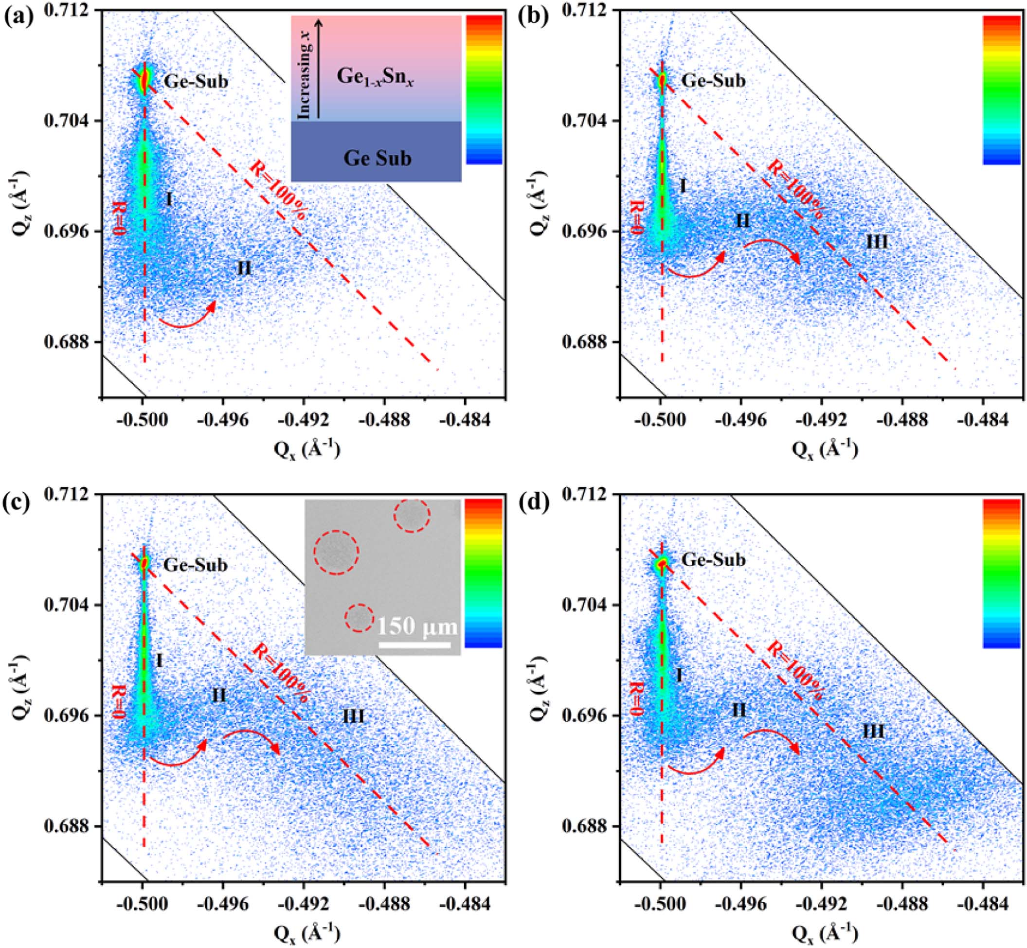
Figure 1.RSM around the asymmetric (
To prove the assumption that the thick GeSn film can still be grown on the relaxed GeSn layer, sample D was prepared with the top GeSn layer thickness of about 200 nm on the same Sn composition gradient layer as sample B. As shown in Fig. 1(d), the top GeSn layer of sample D is fully relaxed, and its Sn composition reaches 16.3%. Sn segregation does not happen in sample D. This indicates that a thick and high-Sn-content GeSn layer can be grown on the relaxed buffer layer.
To confirm the Sn composition and strain state of GeSn samples obtained from RSM, Raman scattering measurements were also performed using a 488 nm incident laser (penetration depth is less than 20 nm in GeSn alloys). For fully relaxed GeSn alloys, the Raman shift of the Ge-Ge longitudinal optical (LO) peak (
![]()
Figure 2.Raman scattering spectra of GeSn samples and a Ge wafer for reference, and the position of the ball corresponds to the calculated Ge-Ge Raman shift.
XTEM tests were conducted to reveal the strain relaxation mechanism in the film. Figure 3(a) shows XTEM images of sample D. No obvious threading defects are observed, and stress fringes appear at the low-Sn-content layer (about 200 nm). The inset of Fig. 3(a) shows energy dispersive X-ray spectroscopy (EDX) Ge and Sn element mapping. The closer to the surface, the more obvious the red color, which directly indicates the increase in Sn composition in GeSn alloys. The top GeSn alloy has uniform Sn composition, and the Sn content is about 16.5% from EDX. Figure 3(b) shows a high-resolution XTEM image of GeSn alloys at the bottom and its fast Fourier transform (FFT) pattern. The clear lattice fringes and typical diffraction pattern evidence the single crystalline layer. It is worth noting that there are some point defects in the GeSn alloys, which can be spotted in the inverse FFT images of Figs. 3(c) and 3(d). The existence of defects makes the lattice arrangement discontinuous and can release the stress caused by the large lattice mismatch.
![]()
Figure 3.(a) Full view of XTEM image of sample D; inset: EDX Ge and Sn element mapping. (b) High-resolution XTEM image and FFT pattern of area “b” in (a). (c), (d) Inverse FFT images of the rectangular area in (b).
Figure 4 demonstrates the SIMS and bandgap calculations of four samples. As expected, the Sn composition is increased gradually along the thickness, which is consistent with the RSM results discussed above. The three region colors are used to represent fully strained, partially relaxed, and fully relaxed states, according to the RSM measurements. From Fig. 4, the rate of Sn composition increase can be divided into the three parts. At the initial growth, the slope of Sn composition increase is about 3.4%/100 nm and changes to about 1.1%/100 nm in the fully strained state. After the sample becomes fully relaxed, the slope of Sn composition increase is enhanced to about 2.5%/100 nm. This indicates that relaxing the strain in the GeSn film can help to incorporate more Sn atoms into the film, which is also observed in GeSn film grown by CVD. As shown in Fig. 4, the thickness of region II (partially relaxed state) for sample A is
![]()
Figure 4.SIMS profile of Sn composition and bandgap calculations at different depths of (a) sample A; (b) sample B; (c) sample C; (d) sample D. Regions marked with different colors correspond to different strain states of the RSM in Fig.
The direct bandgap (
For GeSn films with high Sn content, Sn segregation may easily happen during growth. To investigate the Sn segregation phenomenon in the as-grown Sn gradient GeSn samples, AFM and SEM measurements were performed. The root mean square (RMS) roughness of the GeSn samples is listed in Table 1. The RMS results show that high growth temperature and high Sn composition can cause surface undulations. Moreover, the GeSn layer can maintain its crystal quality by increasing the layer thickness if the GeSn layer is relaxed without Sn segregation. From the SEM results, it is found that only sample C has Sn segregation in some areas [inset of Fig. 1(c)] due to the relatively high Sn content. By decreasing the growth temperature, Sn segregation can also be avoided. Compared with other PVD-grown GeSn work [15,23], the direct growth of GeSn alloys with high Sn composition will generate a large number of threading dislocations, and the Sn surface segregation is severe. The Sn composition graded structure can effectively avoid these problems, which is helpful in growing GeSn alloys with high Sn composition.
So far, relaxed GeSn alloys with high Sn composition were mainly achieved by CVD. The characterization of GeSn materials in this work shows that it is feasible to grow high-Sn-content GeSn films by MBE through applying GeSn buffer layers with gradually increasing Sn content. The thickness of relaxed GeSn alloys with high Sn content can also be further increased on the Sn gradient GeSn structure, which lays the foundation for the preparation of high-performance MIR GeSn devices.
B. Photodetector Analysis
To study the photoelectric performance of the Sn content gradient GeSn film, sample D was used to fabricate a GeSn photodetector. The photodetector has an interdigital electrode structure, and a three-dimensional schematic and top view are shown in Fig. 5(a). As shown in Fig. 5(b), the anode and cathode electrodes are distributed at intervals, forming the electric field points from the anode to cathode when applying voltage. Under light incident conditions, photo-generated carriers are formed in the VB and CB, which are collected by the nearby anode and cathode electrodes. Figure 5(c) shows the symmetrical dark
![]()
Figure 5.(a) Three-dimensional schematic of GeSn photodetector with interdigital electrode structure. The inset shows the top view of the device. (b) Working mechanism of GeSn photodetector under light incident conditions. (c) Dark
Figure 5(d) shows the photocurrent spectra of the GeSn photodetector at 0.2 V for different temperatures. With the increase in temperature, the defects acting as a non-radiative center can be activated, which would lead to a decrease in optical response. Moreover, the intrinsic carrier concentration is also increased as the temperature increases. These can lead to a decrease in the signal-to-noise ratio, and GeSn photodetectors work better in cooling conditions. The signal distortion from 2.58 to 2.77 μm, sudden decrease near 3.36 μm, and jitter around 4.2–4.3 μm are attributed to the absorption of carbon dioxide and water. At 77 K, the cutoff wavelength of the photodetector can reach about 4.2 μm, which is defined based on the intensity decay to 10%. Using a blackbody light source, the intensity value of the photocurrent was tested, and the responsivity of the detector was calibrated. Figure 6(a) shows the wavelength-dependent optical responsivity of the GeSn photodetector under a bias voltage of 1 V at 77 K. The peak wavelength is near 2.53 μm, and its responsivity is about 0.35 A/W. In addition, as the bias voltage increases, the responsivity increases linearly, as shown in the inset of Fig. 6(a). Under a bias voltage of 1 V, the responsivity at 3 μm is up to 226 mA/W.
![]()
Figure 6.(a) Wavelength-dependent optical responsivity of GeSn photodetector under a bias voltage of 1 V at 77 K. Inset: responsivity at 3 μm as a function of voltage at 77 K. (b) Comparison of cutoff wavelength of GeSn photodetectors in different works.
Specific detectivity (
Summary of the Performance of GeSn Photodetectors
| Reference | Sn | Structure | Epitaxial | Peak Specific | Responsivity (A/W) | Cutoff |
|---|---|---|---|---|---|---|
| [ | 3% | PIN | MBE | – | 0.12 at 1.64 μm at −1 V at RT | 1.8 μm |
| [ | 9% | QW/PC | CVD | – | 0.1 at 2.2 μm at 5 V at RT | 2.4 μm |
| [ | 10% | PC | CVD | 1.63 at 1.55 μm at 50 V at 77 K | 2.4 μm | |
| [ | 10% | PIN | CVD | 0.19 at 1.55 μm at − 0.1 V at RT | 2.6 μm | |
| [ | 11% | PC | CVD | 28.5 at 1.55 μm at 2 V at 77 K | 3.0 μm | |
| [ | 20% | PC | CVD | 0.8 at 2.0 μm at 5 V at 77 K | 3.65 μm | |
| [ | 17% | PC | CVD | – | 0.004 at 2.4 μm at | 4.6 μm |
PC is the photoconductor of MSM structure, and PIN is the photodiode of p-i-n structure.
Figure 6(b) shows a comparison of cutoff wavelength of GeSn photodetectors in different works. The detailed performance parameters of GeSn photodetectors are also listed in Table 2. With the development of GeSn material epitaxy technology, the Sn composition in GeSn photodetectors increases, and the cutoff wavelength extends to the MIR (
4. CONCLUSION
Strain-controlled GeSn films were proposed using the method of gradually increasing Sn content along the growth thickness. The Sn composition, strain state, and crystal quality were investigated in detail by RSM, SIMS, and XTEM. At the initial growth, the GeSn alloys were fully strained, and then relaxed rapidly as the Sn composition increased. After the full relaxation process, the Sn content and thickness of GeSn alloys can be further increased without Sn segregation. The
References
[1] A. Rogalski. HgCdTe infrared detector material: history, status and outlook. Rep. Prog. Phys., 68, 2267-2336(2005).
[2] J. P. Clifford, G. Konstantatos, K. W. Johnston, S. Hoogland, L. Levina, E. H. Sargent. Fast, sensitive and spectrally tuneable colloidal-quantum-dot photodetectors. Nat. Nanotechnol., 4, 40-44(2009).
[3] H. S. Kim. Dark current analysis of an InAs/GaSb type II superlattice infrared photodiode with SiO2 passivation. J. Korean Phys. Soc., 78, 1141-1146(2021).
[4] Y. Liu, C. Zhang, X. Wang, J. Wu, L. Huang. Interface investigation of InAs/GaSb type II superlattice for long wavelength infrared photodetectors. Infrared Phys. Technol., 113, 103573(2021).
[5] N. Wang, C. Xue, F. Wan, Y. Zhao, G. Xu, Z. Liu, J. Zheng, Y. Zuo, B. Cheng, Q. Wang. High-performance GeSn photodetector covering all telecommunication bands. IEEE Photon. J., 13, 6800809(2021).
[6] F. Yang, K. Yu, H. Cong, C. Xue, B. Cheng, N. Wang, L. Zhou, Z. Liu, Q. Wang. Highly enhanced SWIR image sensors based on Ge1-
[7] H. Cong, C. L. Xue, J. Zheng, F. Yang, K. Yu, Z. Liu, X. Zhang, B. W. Cheng, Q. M. Wang. Silicon based GeSn p-i-n photodetector for SWIR detection. IEEE Photon. J., 8, 6804706(2016).
[8] X. Li, L. Peng, Z. Liu, Z. Zhou, J. Zheng, C. Xue, Y. Zuo, B. Chen, B. Cheng. 30 GHz GeSn photodetector on SOI substrate for 2 μm wavelength application. Photon. Res., 9, 494-500(2021).
[9] M. Nedeljkovic, J. S. Penades, C. J. Mitchell, A. Z. Khokhar, S. Stankovic, T. D. Bucio, C. G. Littlejohns, F. Y. Gardes, G. Z. Mashanovich. Surface-grating-coupled low-loss Ge-on-Si rib waveguides and multimode interferometers. IEEE Photon. Technol. Lett., 27, 1040-1043(2015).
[10] L. Shen, N. Healy, C. J. Mitchell, J. S. Penades, M. Nedeljkovic, G. Z. Mashanovich, A. C. Peacock. Mid-infrared all-optical modulation in low-loss germanium-on-silicon waveguides. Opt. Lett., 40, 268-271(2015).
[11] T. Hu, B. Dong, X. Luo, T.-Y. Liow, J. Song, C. Lee, G.-Q. Lo. Silicon photonic platforms for mid-infrared applications. Photon. Res., 5, 417-430(2017).
[12] S. Assali, J. Nicolas, O. Moutanabbir. Enhanced Sn incorporation in GeSn epitaxial semiconductors via strain relaxation. J. Appl. Phys., 125, 025304(2019).
[13] W. Dou, M. Benamara, A. Mosleh, J. Margetis, P. Grant, Y. Zhou, S. Al-Kabi, W. Du, J. Tolle, B. Li, M. Mortazavi, S. Q. Yu. Investigation of GeSn strain relaxation and spontaneous composition gradient for low-defect and high-Sn Alloy growth. Sci. Rep., 8, 5640(2018).
[14] F. Wan, C. Xu, X. Wang, G. Xu, B. Cheng, C. Xue. Study of strain evolution mechanism in Ge1-
[15] N. Wang, C. Xue, F. Wan, Y. Zhao, G. Xu, Z. Liu, J. Zheng, Y. Zuo, B. Cheng, Q. Wang. Spontaneously conversion from film to high crystalline quality stripe during molecular beam epitaxy for high Sn content GeSn. Sci. Rep., 10, 6161(2020).
[16] S. Su, B. Cheng, C. Xue, W. Wang, Q. Cao, H. Xue, W. Hu, G. Zhang, Y. Zuo, Q. Wang. GeSn p-i-n photodetector for all telecommunication bands detection. Opt. Express, 19, 6400-6405(2011).
[17] A. Gassenq, F. Gencarelli, J. Van Campenhout, Y. Shimura, R. Loo, G. Narcy, B. Vincent, G. Roelkens. GeSn/Ge heterostructure short-wave infrared photodetectors on silicon. Opt. Express, 20, 27297-27303(2012).
[18] W. Du, T. Pham, J. Margetis, H. Tran, S. A. Ghetmiri, A. Mosleh, G. Sun, R. A. Soref, J. Tolle, H. A. Naseem, B. Li, S.-Q. Yu. Si based mid-infrared GeSn photodetectors and light emitters. Proc. SPIE, 9555, 95550E(2015).
[19] T. Pham, W. Du, H. Tran, J. Margetis, J. Tolle, G. Sun, R. A. Soref, H. A. Naseem, B. Li, S. Q. Yu. Systematic study of Si-based GeSn photodiodes with 2.6 μm detector cutoff for short-wave infrared detection. Opt. Express, 24, 4519-4531(2016).
[20] W. Du, S. Ghetmiri, S. Al-Kabi, A. Mosleh, P. Thach, Y. Zhou, H. Tran, G. Sun, R. Soref, J. Margetis, J. Tolle, B. Li, M. Mortazavi, H. Naseem, S.-Q. Yu. Silicon-based Ge0.89Sn0.11 photodetector and light emitter towards mid-infrared applications. Proc. SPIE, 10108, 1010813(2017).
[21] H. Tran, T. Pham, J. Margetis, Y. Zhou, W. Dou, P. C. Grant, J. M. Grant, S. Al-Kabi, G. Sun, R. A. Soref, J. Tolle, Y.-H. Zhang, W. Du, B. Li, M. Mortazavi, S.-Q. Yu. Si-based GeSn photodetectors toward mid-infrared imaging applications. ACS Photon., 6, 2807-2815(2019).
[22] M. R. M. Atalla, S. Assali, A. Attiaoui, C. Lemieux-Leduc, A. Kumar, S. Abdi, O. Moutanabbir. All-group IV transferable membrane mid-infrared photodetectors. Adv. Funct. Mater., 31, 2006329(2020).
[23] J. Rathore, A. Nanwani, S. Mukherjee, S. Das, O. Moutanabbir, S. Mahapatra. Composition uniformity and large degree of strain relaxation in MBE-grown thick GeSn epitaxial layers, containing 16% Sn. J. Phys. D, 54, 185105(2021).
[24] J. Zheng, W. Huang, Z. Liu, C. Xue, C. Li, Y. Zuo, B. Cheng, Q. Wang. Influence of H2 on strain evolution of high-Sn-content Ge1-
[25] J. Zheng, Z. Liu, Y. Zhang, Y. Zuo, C. Li, C. Xue, B. Cheng, Q. Wang. Growth of high-Sn content (28%) GeSn alloy films by sputtering epitaxy. J. Cryst. Growth, 492, 29-34(2018).
[26] I. Dascalescu, N. C. Zoita, A. Slav, E. Matei, S. Iftimie, F. Comanescu, A. M. Lepadatu, C. Palade, S. Lazanu, D. Buca, V. S. Teodorescu, M. L. Ciurea, M. Braic, T. Stoica. Epitaxial GeSn obtained by high power impulse magnetron sputtering and the heterojunction with embedded GeSn nanocrystals for shortwave infrared detection. ACS Appl. Mater. Interfaces, 12, 33879-33886(2020).
[27] W. Dou, Y. Zhou, J. Margetis, S. A. Ghetmiri, S. Al-Kabi, W. Du, J. Liu, G. Sun, R. A. Soref, J. Tolle, B. Li, M. Mortazavi, S. Q. Yu. Optically pumped lasing at 3 μm from compositionally graded GeSn with tin up to 22.3. Opt. Lett., 43, 4558-4561(2018).
[28] Y. Zhou, W. Dou, W. Du, S. Ojo, H. Tran, S. A. Ghetmiri, J. Liu, G. Sun, R. Soref, J. Margetis, J. Tolle, B. Li, Z. Chen, M. Mortazavi, S.-Q. Yu. Optically pumped GeSn lasers operating at 270 K with broad waveguide structures on Si. ACS Photon., 6, 1434-1441(2019).
[29] Y. Zhou, Y. Miao, S. Ojo, H. Tran, G. Abernathy, J. M. Grant, S. Amoah, G. Salamo, W. Du, J. Liu, J. Margetis, J. Tolle, Y.-H. Zhang, G. Sun, R. A. Soref, B. Li, S.-Q. Yu. Electrically injected GeSn lasers on Si operating up to 100 K. Optica, 7, 924-928(2020).
[30] X. Liu, J. Zheng, M. Li, F. Wan, C. Niu, Z. Liu, Y. Zuo, C. Xue, B. Cheng. Growth of relaxed GeSn film with high Sn content via Sn component-grade buffer layer structure. J. Phys. D, 54, 435101(2021).
[31] C. Xu, P. M. Wallace, D. A. Ringwala, S. L. Y. Chang, C. D. Poweleit, J. Kouvetakis, J. Menéndez. Mid-infrared (3–8 μm) Ge1-
[32] H. H. Tseng, K. Y. Wu, H. Li, V. Mashanov, H. H. Cheng, G. Sun, R. A. Soref. Mid-infrared electroluminescence from a Ge/Ge0.922Sn0.078/Ge double heterostructure p-i-n diode on a Si substrate. Appl. Phys. Lett., 102, 182106(2013).
[33] W. Yu, S. Li, Y. Zhang, W. Ma, T. Sun, J. Yuan, K. Fu, Q. Bao. Near-infrared photodetectors based on MoTe2 /graphene heterostructure with high responsivity and flexibility. Small, 13, 1700268(2017).


Set citation alerts for the article
Please enter your email address

© Copyright 2018-2021 | Chinese Laser Press. All Rights Reserved 沪ICP备15018463号-20