
Moshe Katzman, Maayan Priel, Inbar Shafir, Saawan Kumar Bag, Dvir Munk, Naor Inbar, Moshe Feldberg, Tali Sharabani, Leroy Dokhanian, Matan Slook, Avi Zadok, "Surface acoustic wave photonic filters with a single narrow radio-frequency passband in standard silicon on insulator," Photonics Res. 10, 1723 (2022)
- Photonics Research
- Vol. 10, Issue 7, 1723 (2022)
Abstract
1. INTRODUCTION
Microwave photonics (MWP) research and development address the generation, distribution, and processing of analog radio-frequency signals using optical means [1–3]. Compared with their electronic counterparts, MWP devices and systems may offer broader bandwidths, longer distribution reaches, comparative immunity to electromagnetic interference, and direct incorporation within fiber communication links [1–3]. Applications within advanced wireless and cellular networks demand the production of MWP systems in larger volumes, smaller size, lower cost, and reduced power consumption [4]. These requirements call for the integration of MWP modules at the chip level [5,6]. Silicon photonics is often the medium of choice for MWP devices, due to the promise of co-integration alongside electronic circuits [7,8].
One of the most important functions of MWP processing is the selection of narrowband channels out of broad optical bandwidths [9,10]. A common filter architecture relies on the splitting of signals among multiple paths, referred to as filter taps, and the weighted summation of their delayed replicas [11]. Narrow spectral passbands require long delays in the time-domain. Arbitrarily long delays can be realized over fiber paths; however, their coherent addition is prone to environmental drifting [12]. Chip-level delay-and-sum filters provide stable response; however, integrated-photonic waveguides can only support limited delays due to footprint and loss restrictions. MWP filters have been realized in silicon photonic circuits using ring resonators, Mach–Zehnder interferometers, photonic crystals, and cavities [13–15] (for a review, see Ref. [16]). The transmission bandwidths of silicon-photonic MWP filters range between hundreds of MHz and several GHz [16].
Hypersonic acoustic waves are characterized by wavelengths on the optical scale and frequencies that match the rates of information. Acoustic waves, therefore, represent an excellent candidate platform for MWP signal processing. Highly selective, integrated MWP filters have been realized using acoustic waves. Examples include backward stimulated Brillouin scattering in chalcogenide glass waveguides as part of larger silicon-photonic circuits [17,18], forward Brillouin scattering in suspended silicon membrane waveguides [19,20], and electrical actuation in piezoelectric substrates [21]. Reports include sub-MHz-wide passbands, broad tunability, wide dynamic ranges, and low radio-frequency losses [17–21]. However, these opto-mechanical demonstrations required the supplementing of standard silicon photonics by hybrid material integration or the suspension of structures.
Sign up for Photonics Research TOC. Get the latest issue of Photonics Research delivered right to you!Sign up now
Over the last three years, our group has proposed and demonstrated delay-and-sum MWP filters in standard silicon-on-insulator (SOI) integrated circuits [22–24]. Incoming microwave rate information is converted from the modulation of a first optical carrier to the form of surface acoustic waves (SAWs) through absorption in metallic grating patterns and thermoelastic actuation [25–27]. Information is recovered in the optical domain via photoelastic modulation of a second input optical carrier in a resonator waveguide [22–24]. Slow moving SAWs cross the resonator paths multiple times, imprinting delayed replicas of the input waveform on the output optical carrier. Due to the slow SAWs velocity, delays as long as 175 ns were realized on chip [23,24]. The filter response included up to 12 delayed taps, and the magnitude and radio-frequency phase of each tap could be chosen arbitrarily and independent of those of all others [23]. However, the frequency-domain response of the discrete-time filters consisted of multiple periodic passbands separated by a free spectral range of 65 MHz [23]. In many MWP applications, the selection of a single passband is essential.
In this work, we demonstrate SAW-photonic, discrete-time MWP filters with a single passband of 14 and 7 MHz widths. The number of filter taps is increased to 16 and even 32. The passband frequency can be designed arbitrarily. The experimental results represent a first realization of single-passband, narrow MWP filters in standard SOI, and they further substantiate the SAW-photonic approach for integrated MWP filters with arbitrary transfer functions.
2. PRINCIPLE OF OPERATION
A SAW-photonic, discrete-time integrated MWP filter in SOI is illustrated in Fig. 1. A grating of
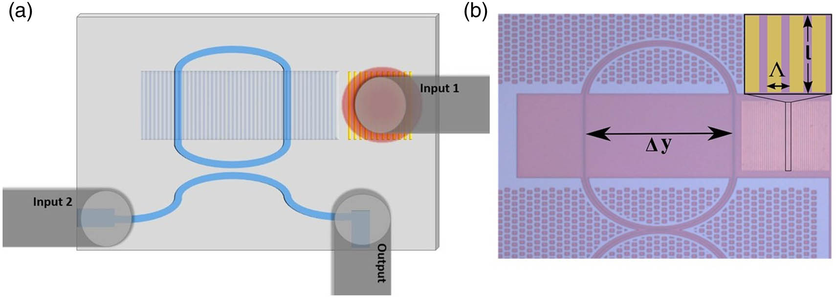
Figure 1.(a) Schematic illustration of a SAW-photonic, discrete-time microwave filter device in SOI. An optical beam (red) from input fiber 1, modulated by microwave-frequency information, illuminates a grating of metallic stripes (yellow). Thermoelastic expansion and contraction of the grating elements lead to the launch of SAWs, which pass across a resonator waveguide layout. Generation of SAWs is the most effective when the grating period and modulation frequency match those of a surface acoustic mode. Continuous-wave light from input fiber 2 is coupled into the resonator waveguide. The propagating SAWs imprint a replica of the input information onto the guided optical wave in each of
SAW actuation is the most efficient for radio-frequency
A resonator waveguide is patterned in proximity to the metallic grating (see Fig. 1). The resonator layout consists of
A second, continuous optical input field is coupled into the resonator waveguide. The exact wavelength of the second input field is locked to a maximal slope of the resonator transfer function [22]. With that alignment, photoelastic modulation along the resonator waveguide is converted to intensity modulation of the guided optical wave at the device output. The normalized time-domain impulse response of the output intensity modulation to SAWs perturbation, in units of
In Eq. (1),
The frequency-domain response
The unitless constant
In Eq. (3),
The constant
The frequency response
The design of a filter device would begin with choosing the grating period
3. EXPERIMENTAL RESULTS
Devices were fabricated in 8 in. (1 in. = 2.54 cm) SOI wafers with a 220-nm-thick silicon device layer and a 2-μm-thick buried oxide layer. Optical waveguides were patterned using UV stepper photolithography and inductively coupled plasma reactive ion etching at the Tower Semiconductor commercial silicon foundry. A ridge waveguide cross section was used, with a partial etching depth of 70 nm and core width of 700 nm. Grating couplers were defined at the edges of bus waveguides leading to the resonators. Metallic gratings were subsequently deposited at Bar-Ilan University facilities, using electron-beam lithography, sputtering, and lift-off processes. The grating stripes comprised a 5-nm-thick chromium adhesion layer followed by a 20-nm-thick gold layer. The metallic grating periods
Figure 2 shows the top-view optical microscope images of 16-tap, 32-tap, and two-tap SAW-photonic devices. The resonators layouts of the 16 (32) tap devices consist of 16 (32) parallel sections with separation
![]()
Figure 2.(a)–(c) Top-view optical microscope images of a 16-tap SAW-photonic MWP filter device. Scale bars correspond to 200 μm, 100 μm, and 50 μm in the three panels, respectively. A square grating of gold stripes is deposited to the right of a long resonator waveguide. The resonator layout consists of 16 straight sections that run parallel to the grating stripes. (d), (e) Top-view optical microscope images of a 32-tap SAW-photonic MWP filter device. Scale bars correspond to 400 μm and 100 μm, respectively. A grating coupler for optical input can be seen at the end of a bus waveguide in the lower left corner of panel (d). A two-tap device to the right of the metallic grating is seen in panel (e).
The transfer functions of optical power through the resonator waveguides of devices under test were characterized using an optical vector network analyzer (VNA), with a spectral resolution of 3 pm. Light was coupled between standard single-mode optical fibers and the bus waveguides of the resonator devices using the grating couplers. The coupling losses were 10 dB per interface. Figure 3(a) shows the measured optical power transfer function of the resonator waveguide in a 32-tap device. The free spectral range of the transfer function is 55 pm. The extinction ratio
![]()
Figure 3.(a) Measured normalized transfer function of optical power through the resonator waveguide of a 32-tap, SAW-photonic microwave filter device. The free spectral range of the transfer function is 55 pm, and its extinction ratio is 15 dB. (b) Experimental setup used in the measurement of MWP filter device transfer functions. EDFA, erbium-doped fiber amplifier; PC, polarization controller; EOM, electro-optic amplitude modulator; CW, continuous-wave. (c) Solid red, measured normalized transfer function
The experimental setup for the characterization of MWP transfer functions of SAW-photonic devices is illustrated in Fig. 3(b). Light from a first laser diode of 1540 nm wavelength passed through an electro-optic Mach–Zehnder intensity modulator (
Continuous-wave light from a second laser diode at 1544 nm wavelength was coupled into the bus waveguide as the second input of the device under test. The exact wavelength of the source was adjusted to a spectral slope of the optical power transfer function of the device [see Fig. 3(a)], using current and temperature tuning. Due to the sharp slope of the transfer function, the input wavelength was actively locked to the slope using a feedback loop (see Appendix A). The second input wave was modulated along the resonator waveguide by SAWs propagating away from the metallic grating. The optical waveform at the device output was amplified by a second EDFA to an average power
The solid red line in Fig. 3(c) shows the measured
Figure 4(a) shows measured transfer functions of two 16-tap devices with different grating periods
![]()
Figure 4.(a) Solid red, measured normalized transfer function
The solid blue trace of Fig. 4(a) presents the measured
The radio-frequency power losses through the devices are large: 95 dB and 100 dB for the 16-tap and 32-tap filters, respectively. Large losses are due to the relative inefficiency of thermoelastic actuation [22,23] and the long lengths
4. SUMMARY AND DISCUSSION
Integrated discrete-time MWP filters with single passbands of 14 and 7 MHz bandwidths were demonstrated in standard SOI photonic circuits. The devices are based on the conversion of radio-frequency modulation information from one optical carrier to another, via SAWs. Due to the slow acoustic velocity, long temporal delays are accumulated over path lengths of few hundreds of micrometers. The current study presents several improvements with respect to our earlier work [23]: the number of taps was increased from a maximum of 12 to 32; the free spectral range of the periodic photoelastic modulation response was extended from 65 to 260 MHz; the probe resonator layout was designed for close spacing between parallel waveguide sections while keeping bending losses at a minimum; and the exact locations of waveguide segments were adjusted to account for optical propagation delays in long resonator sections. Most importantly, these modifications have led to single-passband operation with arbitrary transmission frequency, whereas the response of the previously reported filters consisted of multiple, periodic passbands. Single-passband filters are far more suitable for signal processing applications. The filter bandwidths are comparable with those of Brillouin scattering-based integrated MWP devices [17–20]. The bandwidths are much narrower than those of previous demonstrations of single-passband MWP filters in SOI [13–16].
The main drawback of the proposed devices remains the large losses of radio-frequency electrical power between input and output, measured between 95 and 100 dB. The losses are due to the inherent comparative inefficiency of thermoelastic actuation and increase further by the long lengths
Another drawback of the SAW-photonic devices is that their acoustic frequency of operation
The results of this and previous studies establish SAW-photonics as a potential candidate platform for MWP filters and signal processing. Discrete-time filters with up to 32 coefficients and a single passband have been realized in standard SOI. Furthermore, the complex weight of each filter tap may be chosen arbitrarily and independent of those of all others [23]. In addition to MWP, the devices also serve in the analysis of elastic properties of thin layers and interfaces [24]. Future work will be dedicated to the performance enhancement of the devices, toward achieving lower losses and higher signal-to-noise ratios.
APPENDIX A: ACTIVE LOCKING OF THE INPUT WAVELENGTH TO A SPECTRAL SLOPE OF THE RESONATOR TRANSFER FUNCTION
The conversion of photoelastic phase modulation in the resonator devices into an intensity reading at the output requires that the input wavelength should be aligned with a spectral slope of the optical transfer function. The open-loop adjustment of wavelength to a sharp spectral slope of the resonator response is difficult; hence, active locking was employed instead. A signal at frequency
References
[1] J. Capmany, D. Novak. Microwave photonics combines two worlds. Nat. Photonics, 1, 319-330(2007).
[2] A. Seeds. Microwave photonics. IEEE Trans. Microw. Theory Tech., 50, 877-887(2002).
[3] J. Yao. Microwave photonics. J. Lightwave Technol., 27, 314-335(2009).
[4] R. Waterhouse, D. Novack. Realizing 5G: microwave photonics for 5G mobile wireless systems. IEEE Microw. Mag., 16, 84-92(2015).
[5] D. Marpaung, C. Roeloffzen, R. Heideman, A. Leinse, S. Sales, J. Capmany. Integrated microwave photonics. Laser Photon. Rev., 7, 506-538(2013).
[6] D. Marpaung, J. Yao, J. Capmany. Integrated microwave photonics. Nat. Photonics, 13, 80-90(2019).
[7] L. Pavesi, D. J. Lockwood. Silicon photonics III. Topics in Applied Physics, 119, 1-50(2016).
[8] K. Giewont, K. Nummy, F. A. Anderson, J. Ayala, T. Barwicz, Y. Bian, K. K. Dezfulian, D. M. Gill, T. Houghton, S. Hu, B. Peng, M. Rakowski, S. Rauch, J. C. Rosenberg, A. Sahin, I. Sobert, A. Stricker. 300-mm monolithic silicon photonics foundry technology. IEEE J. Sel. Top. Quantum Electron., 25, 8200611(2019).
[9] J. Capmany, B. Ortega, D. Pastor. A tutorial on microwave photonic filters. J. Lightwave Technol., 24, 201-229(2006).
[10] R. Minasian, E. H. W. Chan, X. Yi. Microwave photonic signal processing. Opt. Express, 21, 22918-22936(2013).
[11] J. Capmany, B. Ortega, D. Pastor, S. Sales. Discrete-time optical processing of microwave signals. J. Lightwave Technol., 23, 702-723(2005).
[12] K. P. Jackson, S. A. Newton, B. Moslehi, M. Tur, C. C. Cutler, J. W. Goodman, H. J. Shaw. Optical fiber delay-line signal processing. IEEE Trans. Microw. Theory Tech., 33, 193-210(1985).
[13] N. Ehteshami, W. Zhang, J. Yao. Optically tunable single passband microwave photonic filter based on phase-modulation to intensity-modulation conversion in a silicon-on-insulator microring resonator. International Topical Meeting on Microwave Photonics (MWP), 1-4(2015).
[14] S. Song, S. X. Chew, X. Yi, L. Nguyen, R. A. Minasian. Tunable single-passband microwave photonic filter based on integrated optical double notch filter. J. Lightwave Technol., 36, 4557-4564(2018).
[15] H. Qiu, F. Zhou, J. Qie, Y. Yao, X. Hu, Y. Zhang, X. Xiao, Y. Yu, J. Dong, X. Zhang. A continuously tunable sub-gigahertz microwave photonic bandpass filter based on an ultra-high-
[16] R. Maram, S. Kaushal, J. Azaña, L. R. Chen. Recent trends and advances of silicon-based integrated microwave photonics. Photonics, 6, 13(2019).
[17] B. J. Eggleton, C. G. Poulton, P. T. Rakich, M. J. Steel, G. Bahl. Brillouin integrated photonics. Nat. Photonics, 13, 664-677(2019).
[18] A. Choudhary, I. Aryanfar, S. Shahnia, B. Morrison, K. Vu, S. Madden, B. Luther-Davies, D. Marpaung, B. J. Eggleton. Tailoring of the Brillouin gain for on-chip widely tunable and reconfigurable broadband microwave photonic filters. Opt. Lett., 41, 436-439(2016).
[19] S. Gertler, E. A. Kittlaus, N. T. Otterstrom, P. T. Rakich. Tunable microwave-photonic filtering with high out-of-band rejection in silicon. APL Photon., 5, 096103(2020).
[20] S. Gertler, E. A. Kittlaus, N. T. Otterstrom, P. Kharel, P. T. Rakich. Microwave filtering using forward Brillouin scattering in photonic-phononic emit-receive devices. J. Lightwave Technol., 38, 5248-5261(2020).
[21] Z. Yu, X. Sun. Acousto-optic modulation of photonic bound state in the continuum. Light Sci. Appl., 9, 1(2020).
[22] D. Munk, M. Katzman, M. Hen, M. Priel, M. Feldberg, T. Sharabani, S. Levy, A. Bergman, A. Zadok. Surface acoustic wave photonic devices in silicon on insulator. Nat. Commun., 10, 4214(2019).
[23] M. Katzman, D. Munk, M. Priel, E. Grunwald, M. Hen, N. Inbar, M. Feldberg, T. Sharabani, R. Zektzer, G. Bashan, M. Vofsi, U. Levy, A. Zadok. Surface acoustic microwave photonic filters in standard silicon-on-insulator. Optica, 8, 697-707(2021).
[24] M. Hen, L. Dokhanian, E. Grunwald, M. Slook, M. Katzman, M. Priel, O. Girshevitz, A. Zadok. Analysis of thin layers using surface acoustic wave-photonic devices in silicon-on-insulator. Opt. Express, 30, 6949-6959(2022).
[25] C. Giannetti, B. Revaz, F. Banfi, M. Montagnese, G. Ferrini, F. Cilento, S. Maccalli, P. Vavassori, G. Oliviero, E. Bontempi, L. E. Depero, V. Metlushko, F. Parmigiani. Thermomechanical behavior of surface acoustic waves in ordered arrays of nanodisks studied by near-infrared pump-probe diffraction experiments. Phys. Rev. B, 76, 125413(2007).
[26] D. Nardi, M. Travagliati, M. E. Siemens, Q. Li, M. M. Murnane, H. C. Kapteyn, G. Ferrini, F. Parimgiani, F. Banfi. Probing thermomechanics at the nanoscale: impulsively excited pseudosurface acoustic waves in hypersonic phononic crystals. Nano Lett., 11, 4126-4133(2011).
[27] M. Schubert, M. Grossman, O. Ristow, M. Hettich, A. Bruchhausen, E. S. C. Barretto, E. Scheer, V. Gusev, T. Dekorsy. Spatial-temporally resolved high-frequency surface acoustic waves on silicon investigated by femtosecond spectroscopy. Appl. Phys. Lett., 101, 013108(2012).
[28] T. Erdogan. Fiber grating spectra. J. Lightwave Technol., 15, 1277-1294(1997).
[29] C. K. Madsen, J. H. Zhao. Optical Filter Design and Analysis(1999).
[30] A. Naiman, B. Desiatov, L. Stern, N. Mazurski, J. Shappir, U. Levy. Ultrahigh-
[31] M. M. de Lima, W. Seidel, H. Kostial, P. V. Santos. Embedded interdigital transducers of high-frequency surface acoustic waves on GaAs. J. Appl. Phys., 96, 3494-3500(2004).
[32] Y. Liu, A. Choudhary, D. Marpaung, B. J. Eggleton. Integrated microwave photonic filters. Adv. Opt. Photon., 12, 485-555(2020).
[33] L. Zhang, L. Jie, M. Zhang, Y. Wang, Y. Xie, Y. Shi, D. Dai. Ultrahigh-
[34] R. Li, L. Zhou, J. Xie, A. Xie, J. Chen. Optimization of adiabatic microring resonators with few-mode and high-
[35] M. M. de Lima, F. Alsina, W. Seidel, P. V. Santos. Focusing of surface acoustic-wave fields on (100) GaAs surfaces. J. Appl. Phys., 94, 7848-7855(2003).
[36] M. M. de Lima, M. Beck, Y. Hey, P. V. Santos. Compact Mach-Zehnder acousto-optic modulator. Appl. Phys. Lett., 89, 121104(2006).
[37] H. Li, S. A. Tadesse, Q. Liu, M. Li. Nanophotonic cavity optomechanics with propagating acoustic waves at frequencies up to 12 GHz. Optica, 2, 826-831(2015).
[38] D. B. Sohn, S. Kim, G. Bahl. Time-reversal symmetry breaking with acoustic pumping of nanophotonic circuits. Nat. Photonics, 12, 91-97(2018).
[39] L. Shao, M. Yu, S. Maity, N. Sinclair, L. Zheng, C. Chia, A. Shams-Ansari, C. Wang, M. Zhang, K. Lai, M. Lončar. Microwave-to-optical conversion using lithium niobate thin-film acoustic resonators. Optica, 6, 1498-1505(2019).


Set citation alerts for the article
Please enter your email address

© Copyright 2018-2021 | Chinese Laser Press. All Rights Reserved 沪ICP备15018463号-20