
Chandraman Patil, Chaobo Dong, Hao Wang, Behrouz Movahhed Nouri, Sergiy Krylyuk, Huairuo Zhang, Albert V. Davydov, Hamed Dalir, Volker J. Sorger. Self-driven highly responsive p-n junction InSe heterostructure near-infrared light detector[J]. Photonics Research, 2022, 10(7): A97
- Photonics Research
- Vol. 10, Issue 7, A97 (2022)
Abstract
1. INTRODUCTION
Two-dimensional (2D) semiconducting materials due to their bandgap have been studied as promising photodetector materials, by changing the layer numbers or forming van der Waals (vdW) heterostructures, owing to their high responsivity, fast response time, broadband photodetection, photodetectivity, and low dark current noise [1–7]. The operation of these high-performance devices demands high bias voltage leading to large power consumption due to the Schottky barrier potential and poor photogenerated carrier collection. This limits technological applications for remote operation conditions under extreme environments, biomedical sensing, and portable devices [8–11]. However, self-driven photodetectors are promising devices to solve energy consumption issues where the photon energy is higher than the bandgap of the material for a better signal-to-noise ratio. Recently, few self-driven 2D material-based photodetectors were demonstrated in Refs. [9,12–14]. III–VI group 2D materials (InSe, GaSe, and GaTe) have been recently studied for light–matter interaction properties for optoelectronic applications [15–17]. 2D InSe, with its direct bandgap () [18], has recently been investigated, showing higher ultrasensitive photodetection characteristics than other 2D semiconducting materials such as and [19–22]. p- and n-doped materials used in heterostructure devices form atomically sharp p-n junctions [23–25].
A thorough study has been performed on InSe-based photodetectors in the visible spectrum but is yet to be explored in detail for near-infrared (NIR) applications [26,27]. Optoelectronic devices for detection, modulation, and sensing applications in the mid-infrared spectrum are also limited by the lack of on-chip sources and the high cost of production [28–30]. Optoelectronic devices based on InSe are usually designed in transistor configuration that requires high electrical bias gating and bias voltage [19,27,31]. Furthermore, the NIR wavelength at 980 nm is widely used for optical humidity sensing fields such as indoor air quality, industrial production process control, and agricultural instrumentation [32,33]. Also, with the technological advancement in building autonomous vehicles, LiDAR-based devices usually are designed at 940–980 nm wavelengths for short to medium range positioning and mapping [34,35]. Due to a direct bandgap (1.25 eV) [18], InSe is an attractive material for manufacturing optoelectronic devices in this range.
Here, we demonstrate a self-driven p-InSe/n-InSe heterostructure photodetector for NIR applications. The p- and n-doped 2D InSe flakes form the vertical heterostructure stack showing a times improvement in responsivity and times lower response time as compared to p- or n-type InSe photodetectors, thus demonstrating a novel fast and sensitive InSe heterojunction-based NIR photodetector suitable for low power optical sensors or detector devices.
Sign up for Photonics Research TOC. Get the latest issue of Photonics Research delivered right to you!Sign up now
2. RESULTS AND DISCUSSION
Enhancing light–matter interaction by building heterostructures using 2D materials paves the way toward building high-performance and energy-efficient compact photodetectors [36]. The 2D material-based photodetectors are often limited by the high bias voltage required for photon-generated carrier collection due to high resistance and the Schottky barrier [37]. Here, we demonstrate a p-n junction-based photodetector using InSe for NIR detection or sensing applications as seen in Fig. 1(a). The 2D InSe flakes are mechanically exfoliated from bulk crystals grown by the vertical Bridgman method and transferred precisely on prefabricated Au/Ti metal contacts using the novel 2D material transfer system discussed in Ref. [38]. The optical microscope image of the device is shown in Fig. 1(b). The p-n InSe heterojunction is formed by the physical contact between Sn-doped InSe (n-type) and Zn-doped InSe (p-type) materials. The band diagram for the device structure can be seen in Fig. 1(c) where the built-in heterojunction potentially helps in collecting the photogenerated carriers in the absence of external electrical bias potential. The material quality was assured after transfer using Raman spectroscopy by monitoring the relative intensities of Raman active modes at , , and [18].
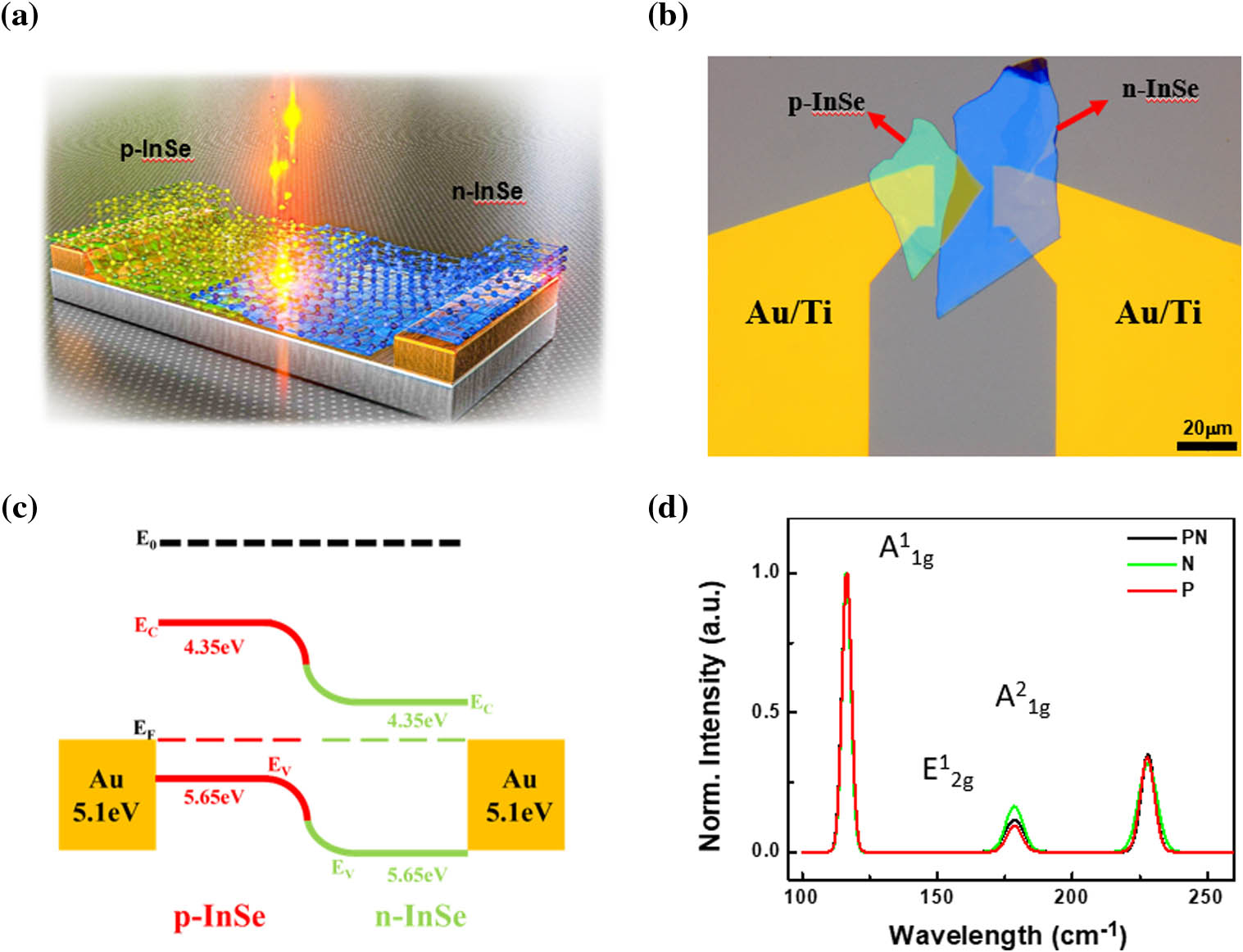
Figure 1.p-n heterojunction n-InSe/p-InSe photodetector. (a) Schematic representation of the n-InSe/p-InSe van der Waals p-n junction photodetector. (b) Optical micrograph image of the device (top view), where n-InSe was stacked on the top of the p-InSe flake, transferred on Au/Ti electrodes using the 2D printer technique. (c) Band diagram for p-InSe (red), n-InSe (green), and Au contact (yellow). (d) Raman spectra of the p-InSe, n-InSe, and the junction regions. All material-associated Raman peaks of p-InSe, n-InSe, and p-n InSe junction are observed to show peak positions and relative intensity associated with out-of-plane vibrational modes (
The photovoltaic properties of the p-InSe/n-InSe heterojunction-based, p-InSe-based, and n-InSe-based photodetector devices are studied at 980 nm under vertical illumination using a free-space optical setup. Figure 2(a) shows the current-voltage (I–V) characteristics for photocurrent measurement of the p-n-InSe junction, p-InSe, and n-InSe, where the illumination power is 111.6 μW. The p-n junction device exhibits an order of magnitude higher photocurrent as compared to the p- and n-InSe devices, thus indicating a higher photo-absorption at 980 nm for the vdW heterojunction characteristics. Figure 2(b) shows the power-dependent photocurrent response of the p-n junction device. It can be observed that the photocurrent saturates after reaching high optical incident power intensity. The photovoltaic effect is attributed to the built-in electric field in the heterojunction depletion region. Figure 2(c) shows the dark current mapped at different voltages for the device. This shows a very small change in the dark current with an increase in the bias voltage leading to low electrical energy loss. As a result of the built-in potential of the junction, the device can be operated under no external bias for collecting photogenerated carriers. Figure 2(d) shows the relationship between the photocurrent and the input optical power for p-n-InSe heterojunction, p-InSe, and n-InSe devices under zero-bias voltage at 980 nm light illumination. It can be seen that the built-in potential in the p-n junction device shows higher photocurrent generation as compared to the non-junction (p- and n-) type devices.
![]()
Figure 2.Photovoltaic characteristics of p-n-InSe heterojunction. (a) Typical
Further, the photodetector devices were tested for responsivity as a function of wavelength from 800 nm to 900 nm (supercontinuum source) and at 980 nm (diode laser) for NIR photodetection. Figure 3(a) shows the responsivity [] of p-n heterojunction, p-, and n-InSe at the zero-bias voltage for the p-n device and at 2 V for p- and n-devices. The p-n junction device shows enhanced responsivity along the NIR wavelength as compared to n- and p-devices by 3.03 times. It can be found that the maximum responsivity of p-InSe/n-InSe heterojunction is about at 980 nm under zero bias. The photoluminescence (PL) spectra of the p-InSe, n-InSe, and p-n-InSe heterojunction from 800 nm to 1000 nm were recorded using a 532 nm laser for excitation. The exciton recombination peak at 980 nm (1.265 eV) in the PL spectrum shows the intensity of p-n-InSe heterojunction higher than that of p-InSe and n-InSe by times at 980 nm as seen in Fig. 3(b). It is known that the exciton PL is very sensitive to the presence of defects and surface contaminants. The enhanced PL intensity at the p-n junction, which is due to the increased photoexcitation volume, provides evidence of a clean interface between the p- and n-InSe flakes. The Raman spectroscopy mapping of the p-n junction stack also confirmed the clean heterojunction formed between the two flakes [Fig. 3(c)]. No additional peaks were observed due to contaminants or defects produced in the material during device fabrication [39].
![]()
Figure 3.Spectral characterization of p-n-InSe heterojunction. (a) Experimental spectra of responsivity of p-InSe, n-InSe, and p-n-InSe heterojunction at 0 V under 800–900 nm and 980 nm light illumination. (b) Photoluminescence spectra of p-InSe, n-InSe, and p-n-InSe heterojunction show strong agreement with the responsivity spectra. An enhancement of 4.5 times and 5.9 times in intensity is observed at 900 nm and 980 nm, respectively. (c) The quality of the heterojunction created was assessed at the
The photoresponse of the p-n-InSe photodetector is expected to be higher than that of the p- and n-InSe due to the built-in potential inside the heterojunction. The on/off switching response for p-n-InSe (0 V), p- (), and n- (2 V) photodetector under 980 nm (111.6 μW) illumination was measured by modulating the optical source power supply. With an increase in the external electric field, the charge density in the InSe is high, leading to a decrease in mobility of photogenerated carriers because of the decrease in carrier drift velocity. The rise and fall time constants of the p-n junction device show a faster response as compared to the p- and n-only InSe photodetectors (Fig. 4). Due to the absence of junction for p- and n-InSe devices, the photocarrier collection is possible only after applying an electrical bias. Therefore, both the devices were tested at 2 V bias for the response time measurement; unlike the built-in electric field of the p-n junction, light-excited electron–hole pairs can be more effectively separated due to the photovoltaic effect versus relying on photoconductivity for the n- and p-only junction devices. The response time of the p-n-InSe device shows a rise time/fall time () response of 8.3 ms/9.6 ms [Fig. 4(a)], which is reduced as compared to n- and p-InSe devices by 18 ms/40 ms [Fig. 4(b)] and 22 ms/29 ms [Fig. 4(c)], respectively. This is an interesting result since it shows the engineerability for designing fast response photodetectors by stacking the 2D materials and enhancing the optoelectronic properties of the material for various applications.
![]()
Figure 4.Time dependent photoresponse of (a) p-n-InSe photodetector at 0 V with rise time/fall time (
The response time of this device is limited by trap states generated in-between material to the substrate and 2D-2D interlayer boundaries. Such trap states help achieve signal detection effectively due to the accumulation of charges but adversely affect the speed response of the device. The trap states generated between the substrate and 2D material majorly contribute to the slow response. This can be improved further by building the device on a 2D substrate material like hBN for preserving the mobility of the material and achieving a faster response time. The low dark current of the device provides a stable noise floor owing to the presence of built-in potential. As seen in Fig. 2(c), the minute change in dark current with an increase in voltage shows that the device can be operated over a varying range of bias voltage without increasing the noise floor of the device. Such device engineering would provide better solutions to lower power sensing and wearable electronics applications.
![]()
Figure 5.Photoresponse mapping under external bias. (a) Photoresponse at different bias voltage (
3. CONCLUSION
A self-driven photodetector was realized for NIR applications at 980 nm, and an extremely low dark current in the range of a few picoamps was achieved. The photoresponse of the 2D InSe was enhanced by building a p-n vdW heterojunction using p- and n-doped InSe showing an increase of times in responsivity as compared to the control n-InSe and p-InSe photodetector devices. The p-n device also exhibits a faster response which is times lower than that of a p- or n-type InSe photodetector, thus demonstrating a novel fast and sensitive InSe heterojunction-based NIR photodetector suitable for low power optical sensors or detector devices. Such performance of this device shows a high potential for realizing an NIR photodetector for sensing and optical applications. Furthermore, by engineering the interlayer stacking to match closely with the lattice structure and improving the metal contact Schottky barrier, it is expected that the device performance in the NIR region will be further improved. Further investigations are required to determine the chemical and mechanical material stability of the InSe heterojunction structure under various environmental effects for applications like remote sensing and biological sensing.
Acknowledgment
Acknowledgment. A. V. D. and S. K. acknowledge support through the Material Genome Initiative funding allocated to the National Institute of Standards and Technology. H. Z. acknowledges support from the U.S. Department of Commerce, National Institute of Standards and Technology under the financial assistance. Disclaimer: Certain commercial equipment, instruments, or materials are identified in this paper to specify the experimental procedure adequately. Such identification is not intended to imply recommendation or endorsement by the National Institute of Standards and Technology, nor is it intended to imply that the materials or equipment identified are necessarily the best available for the purpose.
APPENDIX A: METHODS
InSe single crystals were grown by the vertical Bridgman–Stockbarger method from non-stoichiometric polycrystalline powders. Tin (2% atomic fraction) and Zn (as ZnSe, 0.3% atomic fraction) were added during the powder synthesis to obtain n- and p-typed doped crystals, respectively. The InSe melt in a graphitized quartz ampoule was equilibrated at 720°C for several hours, and then the ampoule was translated across a temperature gradient at a rate of 0.5 mm/h. A representative picture of an InSe ingot is shown in Fig.
![]()
Figure 6.Photograph of a p-InSe ingot cleaved parallel to the
![]()
Figure 7.Atomic resolution annular dark-field scanning transmission electron microscopy (ADF-STEM) image of InSe showing a good match with the overlapped atomic model of
![]()
Figure 8.2D printer transfer setup used for building the p-n heterojunction photodetector.
![]()
Figure 9.Cross-sectional ADF-STEM image of the p-n-InSe photodetector fabricated using the 2D printer transfer setup.
The experimental setup for measuring the 2D InSe p-n junction heterostructure devices comprises a tunable (NKT SUPERCONTINUUM Compact) source and a fixed wavelength laser diode module (CPS980 Thorlabs) at 980 nm wavelength. The light beam was focused on the device using an objective lens. A source meter (Keithley 2600B) was used for electrical response measurements. The response time of the device was measured by modulating the electrical power supply to the laser. The Raman spectrum and PL measurements were performed at room temperature using a 532 nm laser. InSe crystal structure and interface quality of the p-n photodetectors were examined using an FEI Titan 80-300 probe-corrected STEM operating at 300 keV.
References
[1] M. Buscema, D. J. Groenendijk, G. A. Steele, H. S. J. van der Zant, A. Castellanos-Gomez. Photovoltaic effect in few-layer black phosphorus PN junctions defined by local electrostatic gating. Nat. Commun., 5, 4651(2014).
[2] Y. Chen, X. L. Shi, Z. H. Zheng, F. Li, W. D. Liu, W. Y. Chen, X. R. Li, G. X. Liang, J. T. Luo, P. Fan, Z. G. Chen. Two-dimensional WSe2/SnSe p-n junctions secure ultrahigh thermoelectric performance in n-type Pb/I co-doped polycrystalline SnSe. Mater. Today Phys., 16, 100306(2021).
[3] S. Kang, D. Lee, J. Kim, A. Capasso, H. S. Kang, J. W. Park, C. H. Lee, G. H. Lee. 2D semiconducting materials for electronic and optoelectronic applications: potential and challenge. 2D Mater., 7, 022003(2020).
[4] L. Lv, J. Yu, M. Hu, S. Yin, F. Zhuge, Y. Ma, T. Zhai. Design and tailoring of two-dimensional Schottky, PN and tunnelling junctions for electronics and optoelectronics. Nanoscale, 13, 6713-6751(2021).
[5] R. Maiti, C. Patil, M. A. S. R. Saadi, T. Xie, J. G. Azadani, B. Uluutku, R. Amin, A. F. Briggs, M. Miscuglio, D. Van Thourhout, S. D. Solares. Strain-engineered high-responsivity MoTe2 photodetector for silicon photonic integrated circuits. Nat. Photonics, 14, 578-584(2020).
[6] X. Yuan, L. Tang, P. Wang, Z. Chen, Y. Zou, X. Su, C. Zhang, Y. Liu, W. Wang, C. Liu, F. Chen. Wafer-scale arrayed p-n junctions based on few-layer epitaxial GaTe. Nano Res., 8, 3332-3341(2015).
[7] T. Zheng, Z. T. Wu, H. Y. Nan, Y. F. Yu, A. Zafar, Z. Z. Yan, J. P. Lu, Z. H. Ni. Layer-number dependent and structural defect related optical properties of InSe. RSC Adv., 7, 54964-54968(2017).
[8] Y. Wang, J. Pang, Q. Cheng, L. Han, Y. Li, X. Meng, B. Ibarlucea, H. Zhao, F. Yang, H. Liu, H. Liu. Applications of 2D-layered palladium diselenide and its van der Waals heterostructures in electronics and optoelectronics. Nano-Micro Lett., 13, 1(2021).
[9] X. Zhang, J. Shao, C. Yan, X. Wang, Y. Wang, Z. Lu, R. Qin, X. Huang, J. Tian, L. Zeng. High performance broadband self-driven photodetector based on MXene (Ti3C2T
[10] Q. Han, X. Zhao, N. Na, J. Ouyang. Integrating near-infrared visual fluorescence with a photoelectrochemical sensing system for dual readout detection of biomolecules. Anal. Chem., 93, 3486-3492(2021).
[11] Q. Wu, G. Cen, Y. Liu, Z. Ji, W. Mai. A simple-structured silicon photodetector possessing asymmetric Schottky junction for NIR imaging. Phys. Lett. A, 412, 127586(2021).
[12] H. Shang, H. Chen, M. Dai, Y. Hu, F. Gao, H. Yang, B. Xu, S. Zhang, B. Tan, X. Zhang, P. Hu. A mixed-dimensional 1D Se–2D InSe van der Waals heterojunction for high responsivity self-powered photodetectors. Nanoscale Horiz., 5, 564-572(2020).
[13] J. Wu, Z. Yang, C. Qiu, Y. Zhang, Z. Wu, J. Yang, Y. Lu, J. Li, D. Yang, R. Hao, E. Li. Enhanced performance of a graphene/GaAs self-driven near-infrared photodetector with upconversion nanoparticles. Nanoscale, 10, 8023-8030(2018).
[14] Y. Liu, X. Wu, W. Guo, M. Li, X. Niu, J. Yao, Y. Yu, B. Xing, X. Yan, S. Zhang, J. Sha. Self-powered and high responsivity photodetector based on a n-Si/p-GaTe heterojunction. Nanotechnology, 32, 225204(2021).
[15] H. Zhong, Z. Bai, B. Zou. Tuning the luminescence properties of colloidal I–III–VI semiconductor nanocrystals for optoelectronics and biotechnology applications. J. Phys. Chem. Lett., 3, 3167-3175(2012).
[16] Z. Yang, J. Hao. Recent progress in 2D layered III–VI semiconductors and their heterostructures for optoelectronic device applications. Adv. Mater. Technol., 4, 1900108(2019).
[17] C. Ho. Thickness-dependent carrier transport and optically enhanced transconductance gain in III-VI multilayer InSe. 2D Mater., 3, 025019(2016).
[18] M. R. Molas, A. V. Tyurnina, V. Zólyomi, A. K. Ott, D. J. Terry, M. J. Hamer, C. Yelgel, A. Babiński, A. G. Nasibulin, A. C. Ferrari, V. I. Fal’ko. Raman spectroscopy of GaSe and InSe post-transition metal chalcogenides layers. Faraday Discuss., 227, 163-170(2021).
[19] Z. Chen, J. Biscaras, A. Shukla. A high performance graphene/few-layer InSe photo-detector. Nanoscale, 7, 5981-5986(2015).
[20] W. Feng, J. B. Wu, X. Li, W. Zheng, X. Zhou, K. Xiao, W. Cao, B. Yang, J. C. Idrobo, L. Basile, W. Tian. Ultrahigh photo-responsivity and detectivity in multilayer InSe nanosheets phototransistors with broadband response. J. Mater. Chem. C, 3, 7022-7028(2015).
[21] O. Lopez-Sanchez, D. Lembke, M. Kayci, A. Radenovic, A. Kis. Ultrasensitive photodetectors based on monolayer MoS2. Nat. Nanotechnol., 8, 497-501(2013).
[22] D. A. Nguyen, H. M. Oh, N. T. Duong, S. Bang, S. J. Yoon, M. S. Jeong. Highly enhanced photoresponsivity of a monolayer WSe2 photodetector with nitrogen-doped graphene quantum dots. ACS Appl. Mater. Interfaces, 10, 10322-10329(2018).
[23] R. Cheng, D. Li, H. Zhou, C. Wang, A. Yin, S. Jiang, Y. Liu, Y. Chen, Y. Huang, X. Duan. Electroluminescence and photocurrent generation from atomically sharp WSe2/MoS2 heterojunction p–n diodes. Nano Lett., 14, 5590-5597(2014).
[24] S. R. Tamalampudi, Y. Y. Lu, U. R. Kumar, R. Sankar, C. D. Liao, C. H. Cheng, F. C. Chou, Y. T. Chen. High performance and bendable few-layered InSe photodetectors with broad spectral response. Nano Lett., 14, 2800-2806(2014).
[25] F. Wang, Z. Wang, K. Xu, F. Wang, Q. Wang, Y. Huang, L. Yin, J. He. Tunable GaTe-MoS2 van der Waals p–n junctions with novel optoelectronic performance. Nano Lett., 15, 7558-7566(2015).
[26] M. Dai, H. Chen, R. Feng, W. Feng, Y. Hu, H. Yang, G. Liu, X. Chen, J. Zhang, C. Y. Xu, P. Hu. A dual-band multilayer InSe self-powered photodetector with high performance induced by surface plasmon resonance and asymmetric Schottky junction. ACS Nano, 12, 8739-8747(2018).
[27] H. Jang, Y. Seok, Y. Choi, S. H. Cho, K. Watanabe, T. Taniguchi, K. Lee. High-performance near-infrared photodetectors based on surface-doped InSe. Adv. Funct. Mater., 31, 2006788(2021).
[28] E. Heidari, X. Xu, C. J. Chung, R. T. Chen. On-chip Fourier transform spectrometer on silicon-on-sapphire. Opt. Lett., 44, 2883-2886(2019).
[29] E. Heidari, H. Dalir, M. Ahmed, V. J. Sorger, R. T. Chen. Hexagonal transverse-coupled-cavity VCSEL redefining the high-speed lasers. Nanophotonics, 9, 4743-4748(2020).
[30] A. Rostamian, E. Madadi-Kandjani, H. Dalir, V. J. Sorger, R. T. Chen. Towards lab-on-chip ultrasensitive ethanol detection using photonic crystal waveguide operating in the mid-infrared. Nanophotonics, 10, 1675-1682(2021).
[31] L. Liu, L. Wu, A. Wang, H. Liu, R. Ma, K. Wu, J. Chen, Z. Zhou, Y. Tian, H. Yang, C. Shen. Ferroelectric-gated InSe photodetectors with high on/off ratios and photoresponsivity. Nano Lett., 20, 6666-6673(2020).
[32] H. Li, B. Meng, H. Jia, D. Wang, Z. Wei, R. Li, R. Chen. Optical humidity sensor based on ZnO nanomaterials. IEEE 5th Optoelectronics Global Conference (OGC), 169-172(2020).
[33] S. Sikarwar, B. C. Yadav, S. Singh, G. I. Dzhardimalieva, S. I. Pomogailo, N. D. Golubeva, A. D. Pomogailo. Fabrication of nanostructured yttria stabilized zirconia multilayered films and their optical humidity sensing capabilities based on transmission. Sens. Actuators B, 232, 283-291(2016).
[34] H. J. Lee, K. Y. Jung, Y. Kim. Nanostructured Fe2O3/TiO2 composite particles with enhanced NIR reflectance for application to LiDAR detectable cool pigments. RSC Adv., 11, 16834-16840(2021).
[35] A. Jha. A review of visible, near-IR, and mid-IR transitions in rare-earth doped glass waveguides for remote sensing and LIDAR. Proc. SPIE, 6409, 640918(2006).
[36] R. Maiti, C. Patil, R. A. Hemnani, M. Miscuglio, R. Amin, Z. Ma, R. Chaudhary, A. C. Johnson, L. Bartels, R. Agarwal, V. J. Sorger. Loss and coupling tuning via heterogeneous integration of MoS2 layers in silicon photonics. Opt. Mater. Express, 9, 751-759(2019).
[37] C. Patil, R. Maiti, V. J. Sorger. WS2 monolayer integrated photodetector. CLEO: QELS_Fundamental Science, JTh2B.21(2020).
[38] R. A. Hemnani, J. P. Tischler, C. Carfano, R. Maiti, M. H. Tahersima, L. Bartels, R. Agarwal, V. J. Sorger. 2D material printer: a deterministic cross contamination-free transfer method for atomically layered materials. 2D Mater., 6, 015006(2018).
[39] S. Gupta, E. Heintzman, J. Jasinski. Multiphonon Raman spectroscopy properties and Raman mapping of 2D van der Waals solids: graphene and beyond. J. Raman Spectrosc., 46, 217-230(2015).
[40] S. Zhao, J. Wu, K. Jin, H. Ding, T. Li, C. Wu, N. Pan, X. Wang. Highly polarized and fast photoresponse of black phosphorus-InSe vertical p–n heterojunctions. Adv. Funct. Mater., 28, 1802011(2018).
[41] L. Ye, H. Li, Z. Chen, J. Xu. Near-infrared photodetector based on MoS2/black phosphorus heterojunction. ACS Photon., 3, 692-699(2016).
[42] F. Wang, L. Li, W. Huang, L. Li, B. Jin, H. Li, T. Zhai. Submillimeter 2D Bi2Se3 flakes toward high-performance infrared photodetection at optical communication wavelength. Adv. Funct. Mater., 28, 1802707(2018).
[43] D. Kufer, I. Nikitskiy, T. Lasanta, G. Navickaite, F. H. Koppens, G. Konstantatos. Hybrid 2D–0D MoS2–PbS quantum dot photodetectors. Adv. Mater., 27, 176-180(2015).
[44] H. J. Jin, C. Park, K. J. Lee, G. H. Shin, S. Y. Choi. Ultrasensitive WSe2/α-In2Se3 NIR photodetector based on ferroelectric gating effect. Adv. Mater. Technol., 6, 2100494(2021).
[45] M. Hafeez, L. Gan, H. Li, Y. Ma, T. Zhai. Chemical vapor deposition synthesis of ultrathin hexagonal ReSe2 flakes for anisotropic raman property and optoelectronic application. Adv. Mater., 28, 8296-8301(2016).
[46] H. Fu, Z. Li, H. Xie, Z. Sun, B. Wang, H. Huang, G. Han, H. Wang, P. K. Chu, X. F. Yu. Different-sized black phosphorus nanosheets with good cytocompatibility and high photothermal performance. RSC Adv., 7, 14618-14624(2017).
[47] B. Chitara, T. B. Limbu, J. D. Orlando, Y. Tang, F. Yan. Ultrathin Bi2O2S nanosheet near-infrared photodetectors. Nanoscale, 12, 16285-16291(2020).
[48] B. Zheng, Z. Wu, F. Guo, R. Ding, J. Mao, M. Xie, S. P. Lau, J. Hao. Large-area tellurium/germanium heterojunction grown by molecular beam epitaxy for high-performance self-powered photodetector. Adv. Opt. Mater., 9, 2101052(2021).
[49] C. Hsin, S. M. Wang, G. Y. Chen, M. H. Wu, C. W. Huang, S. C. Hsu, S. C. Lo. Si/Ge/Si photodetector by rapid-melting-growth technique. IEEE Trans. Nanotechnol., 17, 607-610(2018).
[50] Z. Huang, T. Zhang, J. Liu, L. Zhang, Y. Jin, J. Wang, K. Jiang, S. Fan, Q. Li. Amorphous MoS2 photodetector with ultra-broadband response. ACS Appl. Electron. Mater., 1, 1314-1321(2019).
[51] H. Tan, C. Fan, L. Ma, X. Zhang, P. Fan, Y. Yang, W. Hu, H. Zhou, X. Zhuang, X. Zhu, A. Pan. Single-crystalline InGaAs nanowires for room-temperature high-performance near-infrared photodetectors. Nano-Micro Lett., 8, 29-35(2016).
[52] C. Patil, H. Dalir, J. H. Kang, A. Davydov, C. W. Wong, V. J. Sorger. Highly accurate, reliable, and non-contaminating two-dimensional material transfer system. Appl. Phys. Rev., 9, 011419(2022).

Set citation alerts for the article
Please enter your email address
© Copyright 2018-2021 | Chinese Laser Press. All Rights Reserved 沪ICP备15018463号-20