
Guowu Zhang, Dan-Xia Xu, Yuri Grinberg, Odile Liboiron-Ladouceur, "Experimental demonstration of robust nanophotonic devices optimized by topological inverse design with energy constraint," Photonics Res. 10, 1787 (2022)
- Photonics Research
- Vol. 10, Issue 7, 1787 (2022)
Abstract
1. INTRODUCTION
Nanophotonic computational design methods have been investigated intensively over the past decades [1–15]. Heuristic methods, such as the genetic algorithm (GA) and particle swarm optimization (PSO) were first investigated and demonstrated in nanophotonic design [16–18]. Later, the adjoint method, which enables efficient gradient calculation with only two optical simulations, was introduced into computational methods for nanophotonic design [19–21]. At the same time, the introduction of level-set [22–26] and density topology [27–30] provided a systematic way to represent design possibilities and, thus, enabled the gradient-based algorithm to further explore the design parameter space. In the level-set method, only the boundary of the design is allowed to be optimized, while in the density topology-based optimization, the permittivity values of the design can be changed continuously providing an enormous design parameter space for the optimization to explore. With such a large possible design space to explore, density topology-based optimization typically converges to a local minimum quickly with remarkable device performance. However, allowing a continuous permittivity poses another problem as intermediate permittivity values do not usually correspond to real materials. To address this problem, several methods are proposed such as adding a binarization process during which the intermediate permittivity values are gradually removed [31], neighbor-biasing [32], and adding an explicit objective function for measuring the binarization of the design [33].
Topologically optimized designs typically include minimum size features that violate the lithography limitations of current nanofabrication technologies. To ensure the optimized designs meet the minimum feature size requirement for a given foundry, several techniques have been proposed. For example, pixel-by-pixel optimization has been proposed and demonstrated where the dimension of a pixel is set to be larger than the predefined minimum feature size [34–36]. Besides, adding minimum length scale control during the optimization process has also been proposed to guarantee the final design’s minimum feature size larger than the predefined value [25,37,38].
Another shortcoming is that the robustness toward fabrication error of the topologically optimized designs is difficult to explicitly optimize. Indeed, the performance of the fabricated devices often deviates from the optimized results. One existing solution is to take into account possible fabrication errors during the optimization process so that the optimized designs still operate well over a certain range of their realizations [39]. However, this inevitably increases the required computational resources.
Sign up for Photonics Research TOC. Get the latest issue of Photonics Research delivered right to you!Sign up now
In our previous work [40], we proposed a novel approach of applying an energy constraint in the optimization process that maximizes the optical energy residing in the silicon regions, or equivalently minimizes the energy inside the surrounding silicon dioxide cladding. By applying energy constraint, the optimization is naturally guided to a nearly binarized device. As most of the energy is confined inside the silicon, less energy will interact with the boundaries. Thus, robustness toward fabrication errors of the final optimized designs is improved. In addition, this constraint inhibits the generation of small features during optimization. Our previously published theoretical work was based on a 2D simulation to illustrate the principle, while in this paper the energy constraint is applied to 3D optimization for experimental device implementation. We demonstrate the benefits of applying energy constraint to the topological optimization of three types of devices: a mode converter (MC), an O-band/C-band duplexer, and a C-band three-channel wavelength division multiplexing (WDM) demultiplexer with 50 nm channel spacing. Specifically, we show how applying energy constraint benefits the binarization of the design during the optimization process, reducing the presence of small features and improving the robustness toward fabrication error. The results of a collection of 15 designs from different inverse design initialization for an O-band/C-band duplexer demonstrate the statistical generality of these improvements. Then, the optimized designs with our proposed energy constraint are fabricated using a commercial electron beam lithography (EBL), and the experimental characterization of the device performance is presented to validate the improvement.
2. OPTIMIZATION RESULTS AND COMPARISON
The proposed devices are designed for fabrication on a silicon-on-insulator (SOI) chip with an optical waveguide thickness of 220 nm. The theoretical basis and 2D algorithm implementation are presented in Ref. [40]. The 3D implementation details are discussed in Appendix A so that we can focus on the optimization and experimental results in the main text. Three different functional devices are optimized in this work, that is an MC, a 1310 nm/1550 nm wavelength duplexer, and a three-channel coarse wavelength division multiplexing (CWDM) demultiplexer with 50 nm channel spacing.
A. Mode Converter
1. Optimization Results for Mode Converter
MCs offer essential optical functions in mode division multiplexing (MDM) systems and are widely used as design prototypical examples for inverse design in the literature [15,30]. In this section, we design an MC between the fundamental transverse electric field (TE0) and the second-order transverse electrical field (TE1). We show how applying energy constraint benefits the binarization of the design during the optimization process, thereby reducing the computation cost.
In our optimization configuration, the fundamental mode (TE0) is excited at the input waveguide, with the goal of generating the next high-order mode (TE1) at the output waveguide. The dimensions of the input and output waveguides, the design region, the cross section of the waveguides, and the position of the monitor (marked by the green dashed line) are shown in Fig. 1. To benchmark our method, the dimension of the design region is selected to be
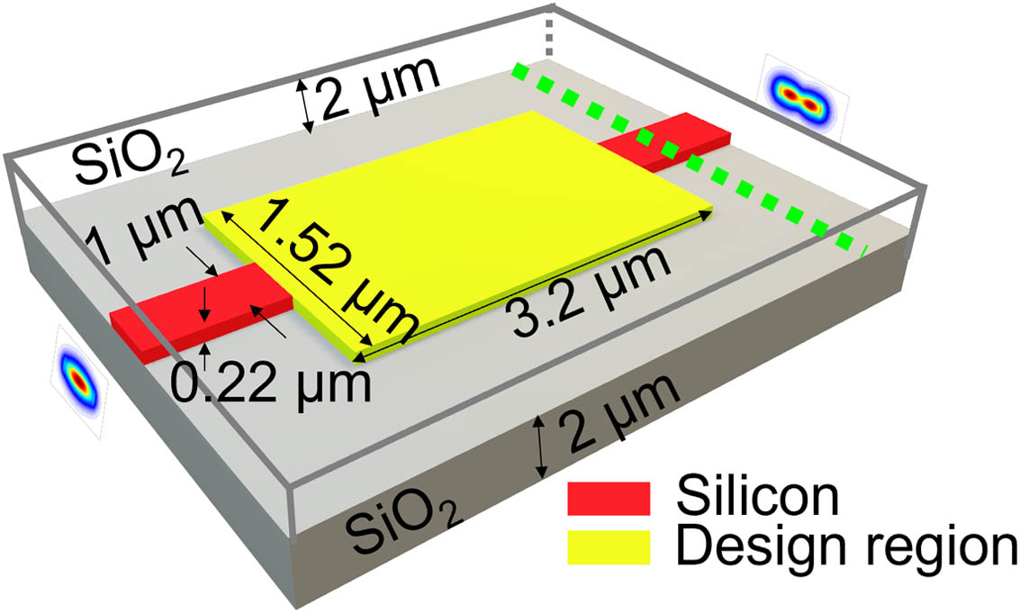
Figure 1.Illustration of the dimensions of the input and output waveguides (in red) and the design region (in yellow) for the TE0 to TE1 mode converter.
For comparison purposes, we investigate three different optimization strategies: gray scale only, baseline, and energy constraint. Each of these optimization strategies is detailed in Appendix A. Fixed computational resources (in this work, it refers to the number of quasi-Newton algorithm iterations, which is 300 for this device) are used for all three optimization strategies. For baseline optimization, the continuous stage and binarization stage take 200 and
The optimization results for the three optimization strategies are shown in Fig. 2. Compared with the gray scale only optimization, applying the energy constraint improves the design binarization. This is observed from the reduction of the intermediate permittivity distribution in the final designs shown in Fig. 2(a). Indeed, the binarization level
![]()
Figure 2.(a) Initial and optimized mode converters for gray scale optimization strategies (note that
Designs from the baseline and energy constraint
2. Experimental Results for Mode Converter
The devices are fabricated using 100 keV EBL at Applied Nanotools (ANT) [44]. The silicon device layer patterning is followed by an inductively coupled plasma-induced reactive ion etching (ICP-RIE) process. A 2.2 μm cladding oxide layer is deposited onto the device using a plasma-enhanced chemical vapor deposition (PECVD) process to protect the silicon layer. The recommended minimum features are specified as 60 nm. The mean and standard width variations for a 500 nm waveguide are found to be 6.295 nm and 1.132 nm, respectively [45]. The correlation length for this variation is found to be 12.23 mm.
The IL and cross talk performance for the fabricated MCs are characterized first. Figures 3(a) and 3(b) show the optical image of the fabricated MC test structures. Figure 3(c) shows the SEM images of the fabricated MC for baseline and energy constraint scenarios. To investigate the IL performance, two, four, six, and eight MCs are cascaded to accumulate enough loss. The IL performance is then calculated from these measurement results using the least squares (LS) regression. The cross talk performance of the MCs is measured using an adiabatic directional coupler (ADC)-based mode multiplexer and demultiplexer to generate the required TE1 modes, a device we previously demonstrated [41]. The measurements are conducted with a testbed comprising a C-band tunable laser (Keysight 8164B), a polarization controller, a 12-channel fiber array, fiber alignment stages, and an optical powermeter. A pair of grating couplers is used to receive (transmit) the light from the single-mode fibers (the chip) onto the chip (the single-mode fiber). All continuous wave (CW) measurements are normalized to a loopback structure that connects two grating couplers with a short waveguide. The measured IL for the loopback structure is approximately 16 dB at 1550 nm.
![]()
Figure 3.Optical image of the test structures for characterizing the mode converter in terms of (a) IL performance and (b) cross talk performance; (c) SEM images for the fabricated design of the baseline (left) and energy constraint strategies (right); (d) measured IL and XT for the mode converter designed by the baseline (solid line) and energy constraint strategies (dashed line); right part shows the zoom in version of the measured IL performance.
Figure 3(d) shows the normalized measured transmission spectrum for the MCs. The results show that the devices optimized with energy constraint perform slightly better than the baseline case. Specifically, the IL at 1550 nm for energy-constrained MC is 0.18 dB whereas 0.34 dB for the baseline case. The corresponding cross talk is
Comparison of the Performance of Mode Converters with the Previous Reported Inversely Designed Mode Converters/Exchangers
| Ref. | Footprint ( | BW (nm) | XT (dB) | IL (dB) | Time (h) | Hardware |
|---|---|---|---|---|---|---|
| [ | 100 | –22.0 | 0.34 | 36 | Intel Core i7-8700 CPU | |
| [ | 40 | –9.1 | 1.34 | 50 | Intel Xeon E5 2697 v3 CPU | |
| This work (baseline) | 100 | –23.0 | 0.34 | 4 | NVidia V100 GPU | |
| This work ( | 100 | –26.7 | 0.18 | 4 | NVidia V100 GPU |
B. Broadband 1310 nm/1550 nm Wavelength Duplexer
1. Optimization Results for 1310 nm/1550 nm Wavelength Duplexer
In this section, a broadband TE mode 1310 nm/1550 nm wavelength duplexer, an important device in WDM systems, is optimized. These wavelength sensitive devices are ideal for quantifying the robustness toward fabrication error since fabrication variations lead to detrimental spectral response shifts [32,40]. The dimensions of the input and output waveguide, the design region, and the position of the monitor (marked using green dashed lines) are shown in Fig. 4(a). The design region is set to
![]()
Figure 4.(a) Illustration of the dimensions of the input and output waveguides (in red) and the design region (in yellow) for the 1310 nm/1550 nm wavelength duplexer; (b) illustration of the wavelength points at which the optimization is conducted for the 1310 nm and 1550 nm channels, respectively.
As was the case for the MC, the gray scale only, baseline, and energy constraint optimizations are investigated. We use 450 quasi-Newton algorithm iterations for all three optimization strategies for this device. For baseline optimization, the continuous stage and binarization stage take 200 and
The optimization results for the three optimization strategies are shown in Fig. 5(a). Similar to the observations made about the MC optimization, applying energy constraint improves the binarization of the design. The field energy distribution in Fig. 5(b) for the baseline (left) and energy constraint optimization (right) strategies shows how the energy is well-confined inside silicon after applying energy constraints and has less interaction with the device boundary. This can be confirmed by the 1550 nm energy (red in the figure) that goes into CH2 passing through several holes (circled using blue dashed line) for the baseline case whereas none was encountered in the energy constraint case. The energy constraint objective function
![]()
Figure 5.(a) Initial and optimized 1310 nm/1550 nm wavelength duplexer layouts for different strategies (note that
We then investigate through simulations the device’s robustness toward fabrication error under different optimization strategies. Specifically, the boundary is biased to
![]()
Figure 6.Simulated transmission spectrum for (a) baseline optimization and (b) the case with energy constraint coefficient
To validate the generality of the above conclusion, another 15 devices from different random initial parameters for baseline and energy constraint strategies are optimized, collected, and analyzed. First, the reduction of small features after applying energy constraint is investigated. The histograms of the minimum feature sizes for the 15 optimizations are shown in Figs. 7(a) and 7(b) for the baseline and energy constraint scenarios. The result shows that these 15 optimizations from the baseline strategy all include minimum features less than 10 nm, which is challenging for today’s fabrication foundry, whereas only a third of them include minimum features less than 10 nm after applying energy constraint. Note that, even though applying energy constraint prevents generating small features, it does this implicitly, which means it cannot guarantee that the minimum feature size of the final design satisfies the fabrication foundry’s requirements. In this case, we believe the optimized design from our energy constraint optimization can be used as a good initial state for further optimization (e.g., length scale optimization [25,37,38]) to meet fabrication requirements. Then, the improvement of the robustness toward fabrication imperfection by applying energy constraint is investigated. This is done by simulating the transmission spectrum of the 15 optimized designs with boundary biased
![]()
Figure 7.Histogram of minimum feature size ranges for (a) 15 baseline optimization runs and (b) 15 runs with an energy constraint coefficient of
After optimization, these designs from the baseline and energy constraint are converted to a GDS file and sent for fabrication. As the fabrication error varies from foundry to foundry or even from different runs of the same foundry, devices with different boundary biases are fabricated. Specifically, to investigate robustness toward fabrication error, for each optimized design, three different versions are included: (1) biased with an over-etching of 10 nm, (2) nominal design, and (3) biased with an under-etching of 10 nm. The measured spectrum shifts for these devices with the intentional fabrication biases illustrate how applying energy constraint improves the robustness of fabricated designs.
2. Experimental Results for 1310 nm/1550 nm Wavelength Duplexer
To characterize the performance of the 1310 nm/1550 nm wavelength duplexer, three tunable lasers (Keysight O-band laser 8164B, Santec ES-band laser TSL-550, Keysight C-band laser 8164B) are used to cover the whole spectrum range from 1260 nm to 1600 nm. Specifically, the available lasers cover 1260 nm to 1350 nm, 1355 nm to 1480 nm, and 1490 nm to 1600 nm, respectively, leaving small gaps in the spectral coverage. Two different grating couplers are used. One covers the O-band, and the other one covers the E-, S-, and C-bands. The fiber array is tilted to the proper angle to maximize the transmission for the given wavelength range. Both baseline and energy constraint optimization are investigated here. The robustness toward fabrication is characterized using the spectrum shifts under certain fabrication errors. Figure 8 provides the randomly chosen SEM images of eight fabricated devices for baseline (top row) and energy constraint (bottom row) scenarios. The structures at the left of the SEM images are used to calibrate the dimension of the device after fabrication.
![]()
Figure 8.SEM images of eight fabricated 1310 nm/1550 nm wavelength duplexers optimized from different random start parameters. Top row, devices from baseline optimization strategy; bottom row, corresponding devices from energy constraint optimization strategy.
![]()
Figure 9.Measured and normalized transmission spectrum of the fabricated 1310 nm/1550 nm wavelength duplexer under
The generality of the improvement in robustness toward
![]()
Figure 10.Measured, normalized, and smoothed transmission spectra of the fabricated 1310 nm/1550 nm wavelength duplexers under different
C. C-Band CWDM Demultiplexer
1. Optimization Results for Three-Channel Demultiplexer
In this section, we optimize a TE mode three-channel C-band CWDM demultiplexer with 50 nm channel spacing which is more complex compared to the MC and the 1310 nm/1550 nm wavelength duplexer [32]. The dimension of the input and output waveguides, the channel specification, and the design region size are shown in Fig. 11(a). The design region is set to
![]()
Figure 11.(a) Illustration of the dimensions of the input and output waveguides (in red) and the design region (in yellow) for the CWDM demultiplexer. (b) Illustration of the wavelength points at which the optimization is conducted for the CH1, CH2, and CH3, respectively.
In this device, only two optimization strategies are considered: gray scale only optimization and energy constraint optimization. The baseline strategy is not included here as it does not converge to a binarized design within the allocated computation resources. Further increasing the iterations in the binarization stage may help, but it will add additional computation resources. Instead of fixing the energy constraint coefficient
The optimization results for the energy constraint with different energy constraint coefficients are shown in Fig. 12. Compared with gray scale only optimization (
![]()
Figure 12.(a) Optimized CWDM demultiplexer layouts for different strategies (note that
![]()
Figure 13.Simulated transmission spectrum of the optimized CWDM demultiplexers under different
![]()
Figure 14.(a) SEM images of the fabricated CWDM demultiplexer for
2. Experimental Results for Three-Channel C-band Demultiplexer
To characterize the performance of the TE mode three-channel C-band CWDM demultiplexer, two tunable lasers (Santec ES-band laser TSL-550, Keysight C-band laser 8164B) are used to cover the spectrum range from 1450 nm to 1650 nm. Moreover, the spectrum shifts under
Figure 14(c) shows the normalized transmission spectrum of the optimized CWDM demultiplexers with energy constraint coefficients 0.5, 0.7, and 0.9. Note that the gap in the transmission spectrum from 1480 nm to 1490 nm is due to the limitation of the tunable bandwidth range for the two tunable lasers, which also applies to all the measurements throughout this paper. The measured ILs are 1.6 dB, 1.5 dB, and 1.8 dB for
Comparison of the Performance of the CWDM Demultiplexers with Previous Reported Inversely Designed CWDM Demultiplexers
| Ref. | Footprint | 1-dB/3-dB | XT (dB) | IL (dB) | Channel | Time (h) | Hardware |
|---|---|---|---|---|---|---|---|
| [ | Not reported | –11.0 | 2.82 | 40 | 60 | NVidia GTX Titan GPU | |
| This work ( | 19/32 | –19.1 | 1.9 | 50 | 48 | NVidia V100 GPU | |
| This work ( | 30/43 | –16.3 | 1.2 | 50 | 48 | NVidia V100 GPU | |
| This work ( | 30/47 | –11.5 | 1.8 | 50 | 48 | NVidia V100 GPU |
The robustness toward fabrication error is investigated next. Figure 15 shows the measured and normalized transmission spectrum for the CWDM demultiplexer under
![]()
Figure 15.Measured transmission spectrum of the fabricated CWDM demultiplexers under different
![]()
Figure 16.Measured spectrum shifts due to
3. CONCLUSION
In summary, we present the experimental validation of the benefits of applying energy constraint in topological inverse design. Both the theoretical implementation details and the experimental results are presented. By applying this constraint, most of the energy stays inside silicon regions providing several advantages. First, it promotes binarization in the optimization process, thereby reducing the required computation resources. Second, it generally increases the size of the features. Finally, it improves robustness to fabrication imperfections due to process variations. Three components are optimized to validate the improvement: (1) a broadband TE0 to TE1 MC, (2) a TE mode 1310 nm/1550 nm wavelength duplexer, and (3) a TE mode three-channel CWDM demultiplexer with 50 nm channel spacing. In the MC example, we demonstrate that the applied energy constraint helps binarize the structure eliminating the additional binarization stage and reducing the number of small features. For the 1310 nm/1550 nm wavelength duplexer, aside from the benefits mentioned above, we also illustrate the improvements to robustness toward fabrication errors when energy constraint is applied. Finally, using the CWDM demultiplexer, we show how robustness toward fabrication imperfections can be further improved by increasing the energy constraint coefficient. We believe our work experimentally validates the benefits of simultaneously optimizing the device’s optical performance as well as the field distribution inside the design region to achieve more practical designs.
APPENDIX A: PRINCIPLES OF INVERSE DESIGN METHOD WITH ENERGY CONSTRAINT
The formalism of the baseline method and the implementation details of the 3D optimization method with our energy constraint are given in this appendix, building on the 2D formulation published previously [
In this paper, the density-based topological method [
![]()
Figure 17.Top view illustration of filtering and projection on a predefined design region (dash blue line): (a) design variable of material distribution
![]()
Figure 18.(a) Illustration of continuous distribution from optimization; (b) illustration of the GDS transferring process using Eq. (
References
[1] J. Lu, J. Vučković. Nanophotonic computational design. Opt. Express, 21, 13351-13367(2013).
[2] A. Y. Piggott, J. Lu, K. G. Lagoudakis, J. Petykiewicz, T. M. Babinec, J. Vučković. Inverse design and demonstration of a compact and broadband on-chip wavelength demultiplexer. Nat. Photonics, 9, 374-377(2015).
[3] S. Molesky, Z. Lin, A. Y. Piggott, W. Jin, J. Vucković, A. W. Rodriguez. Inverse design in nanophotonics. Nat. Photonics, 12, 659-670(2018).
[4] D. Melati, Y. Grinberg, M. K. Dezfouli, S. Janz, P. Cheben, J. H. Schmid, D. X. Xu. Mapping the global design space of nanophotonic components using machine learning pattern recognition. Nat. Commun., 10, 4775(2019).
[5] A. Y. Piggott, E. Y. Ma, L. Su, G. H. Ahn, N. V. Sapra, D. Vercruysse, J. Vuckovic. Inverse-designed photonics for semiconductor foundries. ACS Photon., 7, 569-575(2020).
[6] L. Su, D. Vercruysse, J. Skarda, N. V. Sapra, J. A. Petykiewicz, J. Vučković. Nanophotonic inverse design with SPINS: software architecture and practical considerations. Appl. Phys. Rev., 7, 011407(2020).
[7] B. Shen, P. Wang, R. Polson, R. Menon. An integrated-nanophotonics polarization beamsplitter with 2.4 × 2.4 μm2 footprint. Nat. Photonics, 9, 378-382(2015).
[8] W. Chang, S. Xu, M. Cheng, D. Liu, M. Zhang. Inverse design of a single-step-etched ultracompact silicon polarization rotator. Opt. Express, 28, 28343-28351(2020).
[9] M. P. Bendsoe, O. Sigmund. Topology Optimization: Theory, Methods, and Applications(2013).
[10] J. S. Jensen, O. Sigmund. Topology optimization for nano-photonics. Laser Photon. Rev., 5, 308-321(2011).
[11] S. Yang, H. Jia, L. Zhang, J. Dai, X. Fu, T. Zhou, G. Zhang, L. Yang. Gradient-probability-driven discrete search algorithm for on-chip photonics inverse design. Opt. Express, 29, 28751-28766(2021).
[12] L. Cheng, S. Mao, Z. Chen, Y. Wang, C. Zhao, H. Y. Fu. Ultra-compact dual-mode mode-size converter for silicon photonic few-mode fiber interfaces. Opt. Express, 29, 33728-33740(2021).
[13] N. Zhao, S. Boutami, S. Fan. Efficient method for accelerating line searches in adjoint optimization of photonic devices by combining Schur complement domain decomposition and Born series expansions. Opt. Express, 30, 6413-6424(2022).
[14] S. Boutami, N. Zhao, S. Fan. Determining the optimal learning rate in gradient-based electromagnetic optimization using the Shanks transformation in the Lippmann–Schwinger formalism. Opt. Lett., 45, 595-598(2020).
[15] N. Zhao, S. Boutami, S. Fan. Accelerating adjoint variable method based photonic optimization with Schur complement domain decomposition. Opt. Express, 27, 20711-20719(2019).
[16] Y. Zhang, S. Yang, A. E. J. Lim, G. Q. Lo, C. Galland, T. Baehr-Jones, M. Hochberg. A compact and low loss Y-junction for submicron silicon waveguide. Opt. Express, 21, 1310-1316(2013).
[17] P. Sanchis, P. Villalba, F. Cuesta, A. Håkansson, A. Griol, J. V. Galán, A. Brimont, J. Martí. Highly efficient crossing structure for silicon-on-insulator waveguides. Opt. Lett., 34, 2760-2762(2009).
[18] Y. Zhang, S. Yang, E. J. Lim, G. Lo, T. Baehr-Jones, M. Hochberg. A CMOS-compatible, low-loss and low-crosstalk silicon waveguide crossing. IEEE Photon. Technol. Lett., 25, 422-425(2013).
[19] P. I. Borel, A. Harpøth, L. H. Frandsen, M. Kristensen, P. Shi, J. S. Jensen, O. Sigmund. Topology optimization and fabrication of photonic crystal structures. Opt. Express, 12, 1996-2001(2004).
[20] J. S. Jensen, O. Sigmund. Systematic design of photonic crystal structures using topology optimization: low-loss waveguide bends. Appl. Phys. Lett., 84, 2022-2024(2004).
[21] M. Gerken, D. A. Miller. Multilayer thin-film structures with high spatial dispersion. Appl. Opt., 42, 1330-1345(2003).
[22] C. M. Lalau-Keraly, S. Bhargava, O. D. Miller, E. Yablonovitch. Adjoint shape optimization applied to electromagnetic design. Opt. Express, 21, 21693-21701(2013).
[23] O. D. Miller. Photonic design: from fundamental solar cell physics to computational inverse design(2012).
[24] A. Y. Piggott, J. Petykiewicz, L. Su, J. Vučković. Fabrication-constrained nanophotonic inverse design. Sci. Rep., 7, 1786(2017).
[25] D. Vercruysse, N. V. Sapra, L. Su, R. Trivedi, J. Vučković. Analytical level set fabrication constraints for inverse design. Sci. Rep., 9, 8999(2019).
[26] N. V. Sapra, D. Vercruysse, L. Su, K. Y. Yang, J. Skarda, A. Y. Piggott, J. Vučković. Inverse design and demonstration of broadband grating couplers. IEEE J. Sel. Top. Quantum Electron., 25, 6100207(2019).
[27] L. F. Frellsen, Y. Ding, O. Sigmund, L. H. Frandsen. Topology optimized mode multiplexing in silicon-on-insulator photonic wire waveguides. Opt. Express, 24, 16866-16873(2016).
[28] J. L. P. Ruiz, A. A. Amad, L. H. Gabrielli, A. A. Novotny. Optimization of the electromagnetic scattering problem based on the topological derivative method. Opt. Express, 27, 33586-33605(2019).
[29] J. Huang, J. Yang, D. Chen, X. He, Y. Han, J. Zhang, Z. Zhang. Ultra-compact broadband polarization beam splitter with strong expansibility. Photon. Res., 6, 574-578(2018).
[30] Y. Augenstein, C. Rockstuhl. Inverse design of nanophotonic devices with structural integrity. ACS Photon., 7, 2190-2196(2020).
[31] F. Wang, B. S. Lazarov, O. Sigmund. On projection methods, convergence and robust formulations in topology optimization. Struct. Multidiscip. Optim., 43, 767-784(2011).
[32] L. Su, A. Y. Piggott, N. V. Sapra, J. Petykiewicz, J. Vuckovic. Inverse design and demonstration of a compact on-chip narrowband three-channel wavelength demultiplexer. ACS Photon., 5, 301-305(2018).
[33] O. Sigmund. Morphology-based black and white filters for topology optimization. Struct. Multidiscip. Optim., 33, 401-424(2007).
[34] S. Boutami, S. Fan. Efficient pixel-by-pixel optimization of photonic devices utilizing the Dyson’s equation in a Green’s function formalism. Part I. Implementation with the method of discrete dipole approximation. J. Opt. Soc. Am. B, 36, 2378-2386(2019).
[35] S. Boutami, S. Fan. Efficient pixel-by-pixel optimization of photonic devices utilizing the Dyson’s equation in a Green’s function formalism. Part II. Implementation using standard electromagnetic solvers. J. Opt. Soc. Am. B, 36, 2387-2394(2019).
[36] S. Boutami, K. Hassan, C. Dupré, L. Baud, S. Fan. Experimental demonstration of silicon photonic devices optimized by a flexible and deterministic pixel-by-pixel technique. Appl. Phys. Lett., 117, 071104(2020).
[37] E. Khoram, X. Qian, M. Yuan, Z. Yu. Controlling the minimal feature sizes in adjoint optimization of nanophotonic devices using b-spline surfaces. Opt. Express, 28, 7060-7069(2020).
[38] M. Zhou, B. S. Lazarov, F. Wang, O. Sigmund. Minimum length scale in topology optimization by geometric constraints. Comp. Methods Appl. Mech. Eng., 293, 266-282(2015).
[39] M. Schevenels, B. S. Lazarov, O. Sigmund. Robust topology optimization accounting for spatially varying manufacturing errors. Comp. Methods Appl. Mech. Eng., 200, 3613-3627(2011).
[40] G. Zhang, D.-X. Xu, Y. Grinberg, O. Liboiron-Ladouceur. Topological inverse design of nanophotonic devices with energy constraint. Opt. Express, 29, 12681-12695(2021).
[41] G. Zhang, O. Liboiron-Ladouceur. Scalable and low crosstalk silicon mode exchanger for mode division multiplexing system enabled by inverse design. IEEE Photon. J., 13, 6601013(2021).
[42] H. Jia, T. Zhou, X. Fu, J. Ding, L. Yang. Inverse-design and demonstration of ultracompact silicon meta-structure mode exchange device. ACS Photon., 5, 1833-1838(2018).
[43] A. Michael, E. Yablonovitch. Leveraging continuous material averaging for inverse electromagnetic design. Opt. Express, 26, 31717-31737(2018).
[44] Applied Nanotools. https://www.appliednt.com. https://www.appliednt.com
[45] J. Jhoja, Z. Lu, J. Pond, L. Chrostowski. Efficient layout-aware statistical analysis for photonic integrated circuits. Opt. Express, 28, 7799-7816(2020).
[46] . Lumerical. https://www.lumerical.com/
[47] T. V. Vaerenbergh, P. Sun, S. Hooten, M. Jain, Q. Wilmart, A. Seyedi, R. Beausoleil. Wafer-level testing of inverse-designed and adjoint-inspired vertical grating coupler designs compatible with DUV lithography. Opt. Express, 29, 37021-37036(2021).
[48] O. Sigmund, K. Maute. Topology optimization approaches. Struct. Multidisc. Optim., 48, 1031-1055(2013).
[49] J. P. Groen, C. R. Thomsen, O. Sigmund. Multi-scale topology optimization for stiffness and de-homogenization using implicit geometry modeling. Struct. Multidiscip. Optim., 63, 2919-2934(2021).
[50] K. Svanberg. A class of globally convergent optimization methods based on conservative convex separable approximations. SIAM J. Optim., 12, 555-573(2002).


Set citation alerts for the article
Please enter your email address

© Copyright 2018-2021 | Chinese Laser Press. All Rights Reserved 沪ICP备15018463号-20