• Photonics Research
  • Vol. 10, Issue 7, 1695 (2022)
Tong Wu1, Huifang Zhang2、4、*, Sivaloganathan Kumaran2, Yuehong Xu1, Qingwei Wang1, Wladislaw Michailow2, Xueqian Zhang1、5、*, Harvey E. Beere2、6、*, David A. Ritchie2, and Jiaguang Han1、3、7、*
Author Affiliations
  • 1Center for Terahertz Waves and College of Precision Instrument and Optoelectronics Engineering, Tianjin University, and Key Laboratory of Optoelectronics Information and Technology, Ministry of Education of China, Tianjin 300072, China
  • 2Cavendish Laboratory, University of Cambridge, Cambridge CB3 0HE, UK
  • 3Guangxi Key Laboratory of Optoelectronic Information Processing, School of Optoelectronic Engineering, Guilin University of Electronic Technology, Guilin 541004, China
  • 4e-mail: hz372@cam.ac.uk
  • 5e-mail: alearn@tju.edu.cn
  • 6e-mail: heb1000@cam.ac.uk
  • 7e-mail: jiaghan@tju.edu.cn
  • show less
    DOI: 10.1364/PRJ.462153 Cite this Article Set citation alerts
    Tong Wu, Huifang Zhang, Sivaloganathan Kumaran, Yuehong Xu, Qingwei Wang, Wladislaw Michailow, Xueqian Zhang, Harvey E. Beere, David A. Ritchie, Jiaguang Han. All dielectric metasurfaces for spin-dependent terahertz wavefront control[J]. Photonics Research, 2022, 10(7): 1695 Copy Citation Text show less

    Abstract

    Metasurfaces consisting of artificial subwavelength structure arrays have shown unprecedented ability to manipulate the phase, amplitude, and polarization of light. Separate and complete control over different spin states, namely the orthogonal circular polarizations, has proven more challenging as compared to the control over orthogonal linear polarizations. Here, we present and experimentally demonstrate several spin-dependent wavefront control metasurfaces in the terahertz regime using all-silicon dielectric structures. Such spin-dependent all-silicon metasurfaces are easy to fabricate and have potential applications in spin-involved ultracompact and miniaturized terahertz optical systems as well as terahertz communication systems.

    1. INTRODUCTION

    The spin of a photon is the quantum mechanical counterpart of the polarization of light, and each photon of left-/right-handed circular polarized (LHCP/RHCP) light carries a spin angular momentum of ±, where is the reduced Planck constant [1]. In addition to spin angular momentum (SAM), a photon of circular polarization can also have orbital angular momentum (OAM) which is dependent on the spatial degrees of freedom of light [2], including the intrinsic orbital angular momentum due to optical vortex within the beam and external orbital angular momentum due to the beam propagation in the transverse direction [3]. The spin-orbit interactions (SOIs) between these three types of angular momentums underpin a variety of interesting phenomena [4], including optical spin Hall effect [57], spin-directional coupling [812], and spin-dependent beam shaping [1316], which have potential applications in quantum communication and spin-based optical elements. The underlying physical mechanism of SOI can be explained by the geometric Berry phase originating from the coupling between the SAM and the local coordinates of the media system [17], that is, rotating the transverse x-y coordinates of the inhomogeneous media induces opposite phase shifts for LHCP and RHCP incidences. Conventionally, SOIs have been studied in helical fibers [18], gratings [13], and anisotropic crystals [15]. These systems are either of low efficiency, application-limited, or bulky. Recently, metasurfaces comprising artificial subwavelength planar structures have presented unprecedented abilities to manipulate the polarization, amplitude, and phase of light [19], offering a competitive artificial platform for flexible and considerably enhanced SOI effects [4,20,21].

    The building element of SOI metasurfaces is generally called a Pancharatnam–Berry optical element (PBOE) [13,22]. A perfect PBOE will completely flip the input circular polarization to its orthogonal state with an extra geometric phase shift that is double the element’s orientation angle. Single layer plasmonic metasurfaces were first utilized to study SOI [16,23]. However, their power efficiency was low due to the compromise between anisotropy and transmittance [23]. To increase the SOI efficiency, multilayer plasmonic, coherently controlled, and dielectric metasurfaces have been adopted [22,24,25]. Specifically, dielectric metasurfaces consisting of high contrast dielectric elements have recently attracted increasing research interest [26,27]. For such a dielectric element, the anisotropy is flexibly tailorable over a large range, and the material loss can be made negligible by properly selecting dielectric materials, endowing it with a significant advantage in the search for a perfect PBOE.

    Besides the power efficiency, another challenge of SOI is that the inherent geometric phase shifts of a PBOE over different circularly polarized inputs are equal in magnitude with opposite signs [16]. Therefore, the achieved functionalities are limited only through the geometric phase. To make the imposed phase shifts for RHCP and LHCP inputs independent and thus the spin-control more flexible, further transport phases have been introduced by utilizing PBOEs of various geometries [28]. Through the combination of the transport phase and the geometric phase, independent and complete phase and wavefront control over orthogonal circular polarizations has been demonstrated. Such a method has greatly expanded the applications of PBOEs in polarization optics [2931], including polarization detection [32], splitting [33], polarization contrast imaging [34], multiplexing, and encryption [3537].

    In this context, we present a design method of spin-dependent all-silicon dielectric metasurfaces by simultaneously involving the geometric phase and transport phase in the constituting PBOEs. The PBOEs are anisotropic rectangular posts distributed in a tetragonal lattice on silicon substrate. Two functional metasurface devices are designed and experimentally characterized in the terahertz regime, including a spin-selective Bessel/half-wave metasurface device and a spin-dependent Bessel/vortex beam generator. The Bessel/half-wave metasurface generates a cross-polarized Bessel beam under the LHCP incidence, whereas it only flips the polarization under the RHCP incidence. The Bessel/vortex beam generator produces Bessel and vortex beams separately under the LHCP and RHCP incidences. Such metasurface devices have the potential to help realize miniature THz systems, with key applications in spin switching, contrast imaging, coding, and encryption.

    2. DESIGN STRATEGY

    A perfect PBOE functions as a half-wave plate, i.e., there is a 180° phase difference between the phase shifts along the local fast and slow axes of the PBOE. The corresponding rotated transmission matrix in the Cartesian coordinate system can be expressed as [33] T=[txxtxytyxtyy]=t0R(α)[1001]R(α)=t0eiφf[cos(2α)sin(2α)sin(2α)cos(2α)].Here, the former and latter subscripts of the transmission coefficient tij(i,j=x,y) indicate the polarization directions of the output and input lights, respectively; t0 is the transmission amplitude along the two eigen axes, fast (f) and slow (s); φf is the transport phase shift along the fast axis; and R(α)=[cos(α)sin(α)sin(α)cos(α)] is the rotation matrix, in which α denotes the rotation angle of the PBOE’s local fast axis with respect to the x coordinate. To directly study the spin-dependent response of the PBOE, it is required to further transfer the above matrix into the circular polarization base Tc=[tlltlrtrltrr]=t0[0ei(φf2α)ei(φf+2α)0]=t0[0eiΦlreiΦrl0],where the subscripts l and r indicate LHCP and RHCP, respectively. It is easily seen from Eq. (2) that, with a perfect PBOE, the LHCP light can be completely converted to RHCP light and vice versa. The overall phase shift Φlr for the RHCP incidence equals φf2α, and the overall phase shift Φrl for the LHCP incidence equals φf+2α. In addition to the geometric phase terms 2α and 2α determined by the rotation angle, the output phase shifts for the LHCP and RHCP incidences also contain the transport phase term φf, which is determined by the dimensions of the PBOE element. This provides an effective freedom in decoupling the overall output phases Φlr and Φrl. With the desired Φlr and Φrl, the corresponding required transport phase φf and rotation angle α can be obtained as φf=Φrl+Φlr2,α=ΦrlΦlr4.Thus, by varying φf and α of the PBOEs, complete and independent control over the orthogonal circular polarizations can be achieved. As φf is determined by the geometric parameters, PBOEs of different dimensions are needed to achieve independent phase patterns Φlr and Φrl. Therefore, two key criteria should be taken into consideration: (1) a 180° phase difference between the two local axes with equal transmission amplitudes for every single PBOE is required to ensure perfect cross polarization conversion, and (2) the relative transport phase shifts φf of the PBOEs need to enable the complete 360° phase coverage of Φlr and Φrl.

    (a) Schematic of the spin-dependent metasurface, which consists of PBOEs and can generate two arbitrarily designable beam functions, F1 and F2, under orthogonally circularly polarized incidences. (b) Schematic of a rotated constituent PBOE marked by the red rectangular post in (a). (c) and (d) The simulated transport phase shifts and the corresponding transmission amplitudes of all the 15 PBOEs.

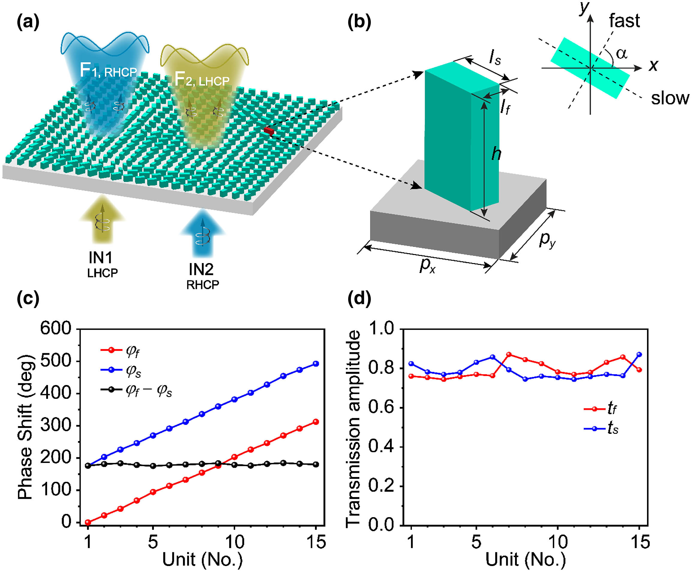
    Figure 1.(a) Schematic of the spin-dependent metasurface, which consists of PBOEs and can generate two arbitrarily designable beam functions, F1 and F2, under orthogonally circularly polarized incidences. (b) Schematic of a rotated constituent PBOE marked by the red rectangular post in (a). (c) and (d) The simulated transport phase shifts and the corresponding transmission amplitudes of all the 15 PBOEs.

    To further investigate the phase control and cross-polarization conversion performances of the 8 fundamental PBOEs, the electric field distributions at 1.0 THz are simulated, as shown in Fig. 2(a). It can be seen that the output phases of Ex and Ey are out of phase in each PBOE, and both of them gradually change by 180° from No. 1 to No. 8. As for the last 7 PBOEs (No. 9 to No. 15), the corresponding simulated electric field distributions under x- and y-polarized incidences are the same as those of the first 7 PBOEs under y- and x-polarized incidences. Figures 2(b) and 2(c) illustrate the simulated transmission amplitude spectra |tyx| and |txx| of the 8 fundamental PBOEs, whereas Fig. 2(d) illustrates the corresponding polarization conversion rates (PCRs) calculated by |tyx|2/(|tyx|2+|txx|2). It can be seen that the y-polarized (cross-polarized) transmissions are obviously larger than those of the x-polarized (co-polarized) transmissions at around 1.0 THz for all PBOEs, where the PCRs all nearly approach 1. To show the cross-polarization conversion performances more clearly, the corresponding |tyx|,|txx|, and PCR values at 1.0 THz marked by the dashed red lines are extracted in Fig. 2(e).

    (a) Simulated electric field distributions of Ex (top row, in the x-z cross section) and Ey (bottom row, in the y-z cross section) at 1.0 THz of the 8 fundamental PBOEs under x- and y-polarized incidences, respectively. (b) and (c) Simulated transmission amplitude spectra |tyx| and |txx| of the 8 fundamental PBOEs (No.1 to No.8) with α=45° under the x-polarized incidence. (d) Calculated PCR of the 8 fundamental PBOEs. (e) Extracted |tyx|, |txx|, and PCR values at 1.0 THz.

    Figure 2.(a) Simulated electric field distributions of Ex (top row, in the x-z cross section) and Ey (bottom row, in the y-z cross section) at 1.0 THz of the 8 fundamental PBOEs under x- and y-polarized incidences, respectively. (b) and (c) Simulated transmission amplitude spectra |tyx| and |txx| of the 8 fundamental PBOEs (No.1 to No.8) with α=45° under the x-polarized incidence. (d) Calculated PCR of the 8 fundamental PBOEs. (e) Extracted |tyx|, |txx|, and PCR values at 1.0 THz.

    3. RESULTS AND DISCUSSION

    To experimentally verify that the selected PBOEs meet the two criteria, i.e., perfect cross-polarization conversion and complete phase coverage, a polarization conversion deflector (PCD) is first constructed by patterning the PBOEs into a linear phase distribution along the x-axis. To enable the complete phase coverage of 360° with a phase increment of 22.5°, the super unit cell comprises 16 PBOEs of which the corresponding phase shifts range from 0° to 337.5° in sequence. Therefore, the periods are Dx=16px=2.4  mm along the x-direction and px=0.15  mm along the y-direction. The orientation angles of all the PBOEs are 45°. Deep reactive ion etching process is employed for the fabrication; see Appendix B. The total size of the fabricated PCD sample is 9.6  mm×9.6  mm, which is the same for all devices in this work. Figure 3(a) shows the optical microscope image of the fractional PCD sample.

    (a) Microscopic image of the fabricated PCD. Scale bar: 300 μm. (b) and (c) The measured normalized intensity distributions as a function of the diffraction angle and the frequency of the y- and x-polarized outputs under x-polarized input, respectively. The white dashed line in (b) indicates the theoretical angles for the +1st diffraction order. (d) The power efficiency of the PCD. The maximum power efficiency appears at 1.1 THz. (e) The normalized intensity profiles of x- and y-polarized output at 1.1 THz.

    Figure 3.(a) Microscopic image of the fabricated PCD. Scale bar: 300 μm. (b) and (c) The measured normalized intensity distributions as a function of the diffraction angle and the frequency of the y- and x-polarized outputs under x-polarized input, respectively. The white dashed line in (b) indicates the theoretical angles for the +1st diffraction order. (d) The power efficiency of the PCD. The maximum power efficiency appears at 1.1 THz. (e) The normalized intensity profiles of x- and y-polarized output at 1.1 THz.

    The PCD was then characterized using our customized all-fiber terahertz time-domain spectrometer (TDS) system [38]. For bandwidth characterization and simplicity, a linearly polarized input is used here. Figures 3(b) and 3(c) show the measured y- and x-polarized outputs under x-polarized input. It can be seen that almost all the x-polarized input is converted to y-polarized light and deflected to the +1st diffraction order, which confirms both the ability to achieve a full phase coverage and the 180° phase difference between φf and φs. Notably, the PCD also supports broadband operation. To illustrate the bandwidth, the power efficiency as a function of frequencies is shown in Fig. 3(d). Here, the power efficiency is defined as the ratio of the output power at the desired polarization and diffraction order to the overall output power. Figure 3(d) highlights that the maximum power efficiency is about 91% and appears at 1.1 THz. The deviation of this operating frequency from the design is likely due to fabrication accuracy. Thus, we focus on the following device performance at 1.1 THz. Figure 3(e) shows the measured normalized intensity curves of the x- and y-polarized outputs at 1.1 THz. The measured deflection angle is θd=6.5°, which coincides with the general Snell's law θd=arcsin(λ/Dx) [39].

    From the measured results of the PCD, it can be concluded that the selected basic PBOEs can well satisfy our requirements in achieving efficient and independent control over the complete phases of the orthogonal circular polarizations at 1.1 THz. Following the above experimental confirmation, we further fabricate two functional devices.

    One is a Bessel/half-wave metasurface, which serves as a Bessel generator under the LHCP incidence but as a half-wave plate under the RHCP incidence. To generate the Bessel beam under the LHCP incidence, a linear gradient of Φrl along the polar coordinate is required, assembling the conventional axicon phase distribution. Therefore, Φrl=2πρarcsin(θB)/λ [40]. Here, ρ is the polar coordinate, and θB indicates the deflection angle of the output light with regards to the optical axis and is dependent on the radial span P of the 360° phase coverage along the polar direction by θB=arcsin(λ/P).

    Meanwhile, attributing to the inherent cross-polarization conversion function of the PBOE metasurface, Φlr does not need any localized alteration but keeps a constant C. Then, the metasurface can be constructed with the selected PBOEs of the transport phase φf=πρarcsin(θB)/λ+C/2 and the rotation angle α=πρarcsin(θB)/(2λ)C/4. Figure 4(a) shows the optical microscope image of the fabricated Bessel/half-wave metasurface for which P is set as 1.24 mm. The metasurface was characterized by a fiber-based near-field scanning THz microscopy (FNSTM) [41]. Figure 4(b) illustrates the measured normalized RHCP intensity profile in the longitudinal plane x=0 under the LHCP incidence from the substrate side. It is clearly seen that there is a typical diffraction-free feature in a distance longer than 30λ along the propagation direction. The transverse normalized intensity and phase profiles at 8 mm above the metasurface are also measured, as shown in Figs. 4(c) and 4(d). Both profiles show typical Bessel features: an intense central spot is surrounded by weak concentric rings due to the limited size of the metasurface, and an almost linear phase gradient along the radial direction. Under the RHCP incidence, the measured longitudinal normalized LHCP intensity, and the transverse normalized intensity and phase profiles are shown in Figs. 4(e)–4(g). It can be observed that the beam keeps propagating as a Gaussian-type wave. Thus, under the RHCP incidence, the metasurface only performs the cross-polarization conversion function as a half-wave plate.

    (a) Microscopic image of a fraction of the fabricated Bessel/half-wave metasurface. Scale bar: 300 μm. (b)–(d) The measured normalized RHCP intensity distributions at the longitudinal propagation plane at x=0 and the intensity and phase profiles at the transverse plane at z=8 mm under the LHCP incidence. (e)–(g) The corresponding measured LHCP distributions under the RHCP incidence. In the measurement, the longitudinal plane spans from −5 to 5 mm along the y-direction and 1 to 12.2 mm along the z-direction, whereas the transverse plane spans from −5 to 5 mm along both the x- and y-directions. The scanning steps are 0.2, 0.2, and 0.4 mm along the x-, y-, and z-directions, respectively.

    Figure 4.(a) Microscopic image of a fraction of the fabricated Bessel/half-wave metasurface. Scale bar: 300 μm. (b)–(d) The measured normalized RHCP intensity distributions at the longitudinal propagation plane at x=0 and the intensity and phase profiles at the transverse plane at z=8  mm under the LHCP incidence. (e)–(g) The corresponding measured LHCP distributions under the RHCP incidence. In the measurement, the longitudinal plane spans from 5 to 5 mm along the y-direction and 1 to 12.2 mm along the z-direction, whereas the transverse plane spans from 5 to 5 mm along both the x- and y-directions. The scanning steps are 0.2, 0.2, and 0.4 mm along the x-, y-, and z-directions, respectively.

    The second device is a Bessel/vortex metasurface, which is capable of producing Bessel and vortex beams separately by switching between the LHCP and RHCP incidences. The Bessel beam for the LHCP input is designed to the same specifications as the former device, while the first-order vortex beam for the RHCP input is designed with a topological charge +1 by Φlr=θ [42], where θ is the azimuthal angle. Using the same design principle, we can obtain the φf and α required to be patterned on the metasurface. Figure 5(a) shows the optical microscope image of the fabricated sample. Under the LHCP incidence, the measured normalized RHCP longitudinal normalized intensity profile at x=0 is illustrated in Fig. 5(b). Figures 5(c) and 5(d) illustrate the transverse intensity and phase profiles at z=5  mm. Similar Bessel features are observed as those seen in Figs. 4(b), 4(c), and 4(d). Figure 5(e) illustrates the measured normalized LHCP longitudinal intensity profile at x=0, and Figs. 5(f) and 5(g) illustrate the transverse intensity and phase profiles at z=8  mm, under the RHCP incidence. Two distinct divergent lobes can be seen from the longitudinal propagation plane, in which the intensity along their central line is almost 0. Meanwhile, the transverse intensity profile in Fig. 5(f) presents a doughnut spot, and the phase profile presents a helical phase of 360° encircling the phase singularity at the center. These features coincide with the +1st vortex beam as expected.

    (a) Microscopic image of a fraction of the fabricated Bessel/vortex metasurface. Scale bar: 300 μm. (b)–(d) The measured normalized RHCP intensity distributions at the longitudinal propagation plane at x=0, and the intensity and phase profiles at the transverse plane at z=5 mm under LHCP incidence. (e)–(g) The corresponding measured LHCP distributions under the RHCP incidence, in which the transverse plane is at z=8 mm.

    Figure 5.(a) Microscopic image of a fraction of the fabricated Bessel/vortex metasurface. Scale bar: 300 μm. (b)–(d) The measured normalized RHCP intensity distributions at the longitudinal propagation plane at x=0, and the intensity and phase profiles at the transverse plane at z=5  mm under LHCP incidence. (e)–(g) The corresponding measured LHCP distributions under the RHCP incidence, in which the transverse plane is at z=8  mm.

    4. CONCLUSION

    Terahertz all-silicon dielectric metasurfaces for spin-dependent and complete wavefront control are realized using PBOEs through introducing extra geometry inhomogeneity besides the rotation inhomogeneity. In this work, a simplified design strategy is utilized to facilitate the metasurface design attributing to the structure symmetry. Based on the simplified design, several exemplar metasurfaces are accomplished using the minimized fundamental constituting elements. One is used to confirm the performance of the selected PBOEs, while the other two metasurfaces demonstrate functional devices—a Bessel/half-wave metasurface and a Bessel/vortex metasurface. The measured results agree well with our design. Such dielectric metasurfaces are easy to fabricate, compatible with semiconductor integration, and have promising applications in ultra-compact and spin-involved optical terahertz imaging system and communication systems for polarization contrast imaging, coding, and encryption.

    APPENDIX A: SIMULATION METHODS

    To select the proper PBOEs, CST Microwave Studio is used to simulate the transmissions (including amplitude and shift) of the silicon posts, in which we set α=0° and raster scan the lateral dimensions lf and ls. Periodic boundaries are applied along the x- and y-directions. Plane waves of x and y polarizations separately illuminate the structure layer from the substrate side. The corresponding outputs are detected using probes positioned at the far-field on the air side. After getting all the simulated transmissions, we selected the proper 15 PBOEs required for an 8-level phase control at 1.0 THz; see Table 1. The presented phase shifts in Fig. 1(c) are plotted by taking the φf of the first PBOE (lf=93.5  μm, ls=50  μm) as the reference, as it is the relative phase shifts that matter for the polarization and wavefront control. The electric field distributions in Fig. 2(a) are obtained by setting the field monitor at 1.0 THz in simulation.

    APPENDIX B: SAMPLE FABRICATION

    The silicon dielectric metasurfaces were fabricated using conventional photolithography and deep reactive ion etching (DRIE) [43]. The silicon wafer used here is a 100-orientation, double-side-polished, high-resistivity (resistivity>10000  Ω·cm) 1-mm-thick wafer. First, the wafer was cleaned using a standard Radio Corporation of America (RCA) process. Next, a thin layer of photoresist (AZ460) was spun on the wafer at 3000 r/min for 40 s and baked at 120°C for 2 min. After that, conventional photolithography was performed to transfer the pattern from a predesigned quartz-chrome mask to the photoresist. Subsequently, the wafer was developed in a developer (400 K) for 18 s. After rinsing it in ultra-pure water for 20 min, the remained photoresist pattern was again baked at 120°C for 2 min. Then, the unprotected silicon parts were etched with a depth of 200 μm using an inductive coupled plasma etcher (Sentech, ICP-RIE SI 500). Finally, the residual photoresist was chemically removed with an acetone and methyl alcohol solution.

    References

    [1] A. I. Akhiezer, V. B. Berestetskii. Quantum Electrodynamics(1965).

    [2] J. Allen, S. M. Barnett, M. J. Padgett. Optical Angular Momentum(2003).

    [3] A. T. O’Neil, I. MacVicar, L. Allen, M. J. Padgett. Intrinsic and extrinsic nature of the orbital angular momentum of a light beam. Phys. Rev. Lett., 88, 053601(2002).

    [4] K. Y. Bliokh, F. J. Rodríguez-Fortuño, F. Nori, A. V. Zayats. Spin-orbit interactions of light. Nat. Photonics, 9, 796-808(2015).

    [5] M. Onoda, S. Murakami, N. Nagaosa. Hall effect of light. Phys. Rev. Lett., 93, 083901(2004).

    [6] O. Hosten, P. Kwiat. Observation of the spin Hall effect of light via weak measurements. Science, 319, 787-790(2008).

    [7] K. Y. Bliokh, A. Niv, V. Kleiner, E. Hasman. Geometrodynamics of spinning light. Nat. Photonics, 2, 748-753(2008).

    [8] S.-Y. Lee, I.-M. Lee, J. Park, S. Oh, W. Lee, K.-Y. Kim, B. Lee. Role of magnetic induction currents in nanoslit excitation of surface plasmon polaritons. Phys. Rev. Lett., 108, 213907(2012).

    [9] N. Shitrit, I. Yulevich, E. Maguid, D. Ozeri, D. Veksler, V. Kleiner, E. Hasman. Spin-optical metamaterial route to spin-controlled photonics. Science, 340, 724-726(2013).

    [10] J. Lin, J. P. B. Mueller, Q. Wang, G. Yuan, N. Antoniou, X.-C. Yuan, F. Capasso. Polarization-controlled tunable directional coupling of surface plasmon polaritons. Science, 340, 331-334(2013).

    [11] F. J. Rodríguez-Fortuño, I. Barber-Sanz, D. Puerto, A. Griol, A. Martínez. Resolving light handedness with an on-chip silicon microdisk. ACS Photon., 1, 762-767(2014).

    [12] X. Zhang, Y. Xu, W. Yue, Z. Tian, J. Gu, Y. Li, R. Singh, S. Zhang, J. Han, W. Zhang. Anomalous surface wave launching by handedness phase control. Adv. Mater., 27, 7123-7129(2015).

    [13] Z. Bomzon, G. Biener, V. Kleiner, E. Hasman. Space-variant Pancharatnam–Berry phase optical elements with computer-generated subwavelength gratings. Opt. Lett., 27, 1141-1143(2002).

    [14] G. Biener, A. Niv, V. Kleiner, E. Hasman. Formation of helical beams by use of Pancharatnam–Berry phase optical elements. Opt. Lett., 27, 1875-1877(2002).

    [15] L. Marrucci, C. Manzo, D. Paparo. Optical spin-to-orbital angular momentum conversion in inhomogeneous anisotropic media. Phys. Rev. Lett., 96, 163905(2006).

    [16] L. Huang, X. Chen, H. Mühlenbernd, G. Li, B. Bai, Q. Tan, G. Jin, T. Zentgraf, S. Zhang. Dispersionless phase discontinuities for controlling light propagation. Nano Lett., 12, 5750-5755(2012).

    [17] S. I. Vinitskiĭ, V. L. Derbov, V. M. Dubovik, B. L. Markovski, Y. P. Stepanovskiĭ. Topological phases in quantum mechanics and polarization optics. Sov. Phys. Uspekhi, 33, 403-428(1990).

    [18] A. Tomita, R. Y. Chiao. Observation of Berrys topological phase by use of an optical fiber. Phys. Rev. Lett., 57, 937-940(1986).

    [19] N. Yu, F. Capasso. Flat optics with designer metasurfaces. Nat. Mater., 13, 139-150(2014).

    [20] S. Xiao, J. Wang, F. Liu, S. Zhang, X. Yin, J. Li. Spin-dependent optics with metasurfaces. Nanophotonics, 6, 215-234(2017).

    [21] X. Yu, X. Wang, Z. Li, L. Zhao, F. Zhou, J. Qu, J. Song. Spin Hall effect of light based on a surface plasmonic platform. Nanophotonics, 10, 3031-3048(2021).

    [22] D. Lin, P. Fan, E. Hasman, M. L. Brongersma. Dielectric gradient metasurface optical elements. Science, 345, 298-302(2014).

    [23] G. Li, M. Kang, S. Chen, S. Zhang, E. Y.-B. Pun, K. W. Cheah, J. Li. Spin-enabled plasmonic metasurfaces for manipulating orbital angular momentum of light. Nano Lett., 13, 4148-4151(2013).

    [24] G. Zheng, H. Mühlenbernd, M. Kenney, G. Li, T. Zentgraf, S. Zhang. Metasurface holograms reaching 80% efficiency. Nat. Nanotechnol., 10, 308-312(2015).

    [25] H. Zhang, M. Kang, X. Zhang, W. Guo, C. Lv, Y. Li, W. Zhang, J. Han. Coherent control of optical spin-to-orbital angular momentum conversion in metasurface. Adv. Mater., 29, 1604252(2017).

    [26] P. Genevet, F. Capasso, F. Aieta, M. Khorasaninejad, R. Devlin. Recent advances in planar optics: from plasmonic to dielectric metasurfaces. Optica, 4, 139-152(2017).

    [27] Y. Hu, X. Wang, X. Luo, X. Ou, L. Li, Y. Chen, P. Yang, S. Wang, H. Duan. All-dielectric metasurfaces for polarization manipulation: principles and emerging applications. Nanophotonics, 9, 3755-3780(2020).

    [28] J. P. Balthasar Mueller, N. A. Rubin, R. C. Devlin, B. Groever, F. Capasso. Metasurface polarization optics: independent phase control of arbitrary orthogonal states of polarization. Phys. Rev. Lett., 118, 113901(2017).

    [29] X. Luo, X. Li, M. Pu, Y. Guo, F. Zhang, X. Ma. Symmetric and asymmetric photonic spin-orbit interaction in metasurfaces. Prog. Quantum Electron., 79, 100344(2021).

    [30] F. Ding, S. Tang, S. I. Bozhevolnyi. “Recent advances in polarization-encoded optical metasurfaces. Adv. Photon. Res., 2, 2000173(2021).

    [31] Y. Qiu, S. Tang, T. Cai, H. Xu, F. Ding. Fundamentals and applications of spin-decoupled Pancharatnam–Berry metasurfaces. Front. Optoelectron., 14, 134-147(2021).

    [32] Y. Guo, S. Zhang, M. Pu, Q. He, J. Jin, M. Xu, Y. Zhang, P. Gao, X. Luo. Spin-decoupled metasurface for simultaneous detection of spin and orbital angular momenta via momentum transformation. Light Sci. Appl., 10, 63(2021).

    [33] Y. Xu, Q. Li, X. Zhang, M. Wei, Q. Xu, Q. Wang, H. Zhang, W. Zhang, C. Hu, Z. Zhang, C. Zhang, X. Zhang, J. Han, W. Zhang. Spin-decoupled multifunctional metasurface for asymmetric polarization generation. ACS Photon., 6, 2933-2941(2019).

    [34] P. Huo, C. Zhang, W. Zhu, M. Liu, S. Zhang, S. Zhang, L. Chen, H. J. Lezec, A. Agrawal, Y. Lu, T. Xu. Photonic spin-multiplexing metasurface for switchable spiral phase contrast imaging. Nano Lett., 20, 2791-2798(2020).

    [35] H.-X. Xu, L. Han, Y. Li, Y. Sun, J. Zhao, S. Zhang, C.-W. Qiu. Completely spin-decoupled dual-phase hybrid metasurfaces for arbitrary wavefront control. ACS Photon., 6, 211-220(2018).

    [36] T. Li, X. Li, S. Yan, X. Xu, S. Wang, B. Yao, Z. Wang, S. Zhu. Generation and conversion dynamics of dual Bessel beams with a photonic spin-dependent dielectric metasurface. Phys. Rev. Appl., 15, 014059(2021).

    [37] C. Zheng, J. Li, G. Wang, J. Li, S. Wang, M. Li, H. Zhao, Z. Yue, Y. Zhang, Y. Zhang, J. Yao. All-dielectric chiral coding metasurface based on spin-decoupling in terahertz band. Nanophotonics, 10, 1347-1355(2021).

    [38] H. Zhang, X. Zhang, Q. Xu, C. Tian, Q. Wang, Y. Xu, Y. Li, J. Gu, Z. Tian, C. Ouyang, X. Zhang, C. Hu, J. Han, W. Zhang. High-efficiency dielectric metasurfaces for polarization-dependent terahertz wavefront manipulation. Adv. Opt. Mater., 6, 1700773(2018).

    [39] N. Yu, P. Genevet, M. A. Kats, F. Aieta, J.-P. Tetienne, F. Capasso, Z. Gaburro. Light propagation with phase discontinuities: Generalized laws of reflection and refraction. Science, 334, 333-337(2011).

    [40] F. Aieta, P. Genevet, M. A. Kat, N. Yu, R. Blanchard, Z. Gaburro, F. Capasso. Aberration-free ultrathin flat lenses and axicons at telecom wavelengths based on plasmonic metasurfaces. Nano Lett., 12, 4932-4936(2012).

    [41] H. Zhang, X. Zhang, Q. Xu, Q. Wang, Y. Xu, M. Wei, Y. Li, J. Gu, Z. Tian, C. Ouyang, X. Zhang, C. Hu, J. Han, W. Zhang. Polarization-independent all-silicon dielectric metasurfaces in the terahertz regime. Photon. Res., 6, 24-29(2018).

    [42] L. Allen, M. W. Beijersbergen, R. J. C. Spreeuw, J. P. Woerdman. Orbital angular momentum of light and the transformation of Laguerre-Gaussian laser modes. Phys. Rev. A, 45, 8185-8189(1992).

    [43] M. Huff. Recent advances in reactive ion etching and applications of high-aspect-ratio microfabrication. Micromachines, 12, 991(2021).

    Tong Wu, Huifang Zhang, Sivaloganathan Kumaran, Yuehong Xu, Qingwei Wang, Wladislaw Michailow, Xueqian Zhang, Harvey E. Beere, David A. Ritchie, Jiaguang Han. All dielectric metasurfaces for spin-dependent terahertz wavefront control[J]. Photonics Research, 2022, 10(7): 1695
    Download Citation