Contents
2022
Volume: 10 Issue 6
22 Article(s)

Export citation format
NEXT-GENERATION SILICON PHOTONICS
Silicon nitride passive and active photonic integrated circuits: trends and prospects
Chao Xiang, Warren Jin, and John E. Bowers
The use of silicon nitride in integrated photonics has rapidly progressed in recent decades. Ultra-low-loss waveguides based on silicon nitride are a favorable platform for the research of nonlinear and microwave photonics and their application to a wide variety of fields, including precision metrology, communications, sensing, imaging, navigation, computation, and quantum physics. In recent years, the integration of Si and III-V materials has enabled new large-scale, advanced silicon nitride-based photonic integrated circuits with versatile functionality. In this perspective article, we review current trends and the state-of-the-art in silicon nitride-based photonic devices and circuits. We highlight the hybrid and heterogeneous integration of III-V with silicon nitride for electrically pumped soliton microcomb generation and ultra-low-noise lasers with fundamental linewidths in the tens of mHz range. We also discuss several ultimate limits and challenges of silicon nitride-based photonic device performance and provide routes and prospects for future development.
Photonics Research
  • Publication Date: May. 20, 2022
  • Vol. 10, Issue 6, A82 (2022)
Research Articles
Fiber Optics and Optical Communications
Multiphoton ionization of standard optical fibers
M. Ferraro, F. Mangini, Y. Sun, M. Zitelli, A. Niang, M. C. Crocco, V. Formoso, R. G. Agostino, R. Barberi, A. De Luca, A. Tonello, V. Couderc, S. A. Babin, and S. Wabnitz
Atoms ionization by the simultaneous absorption of multiple photons has found applications in fiber optics, where it leads to unique nonlinear phenomena. To date, studies of the ionization regime have been limited to gas-filled hollow-core fibers. Here, we investigate multiphoton ionization of standard optical fibers, where intense laser pulses ionize the atoms constituting the fiber structure itself, instead of that of the filling gas. We characterize material modifications produced by optical breakdown. Their formation affects laser beam dynamics over hours long temporal scales. The damage features are studied by means of optical microscopy and X-ray microtomography. In the framework of glass photonics, our results pave the way for a novel glass waveguide micromachining technique.
Photonics Research
  • Publication Date: May. 12, 2022
  • Vol. 10, Issue 6, 1394 (2022)
Imaging Systems, Microscopy, and Displays
Metalens-based stereoscopic microscope
Yong Long, Jianchao Zhang, Zhihao Liu, Weibin Feng, Songming Guo, Qian Sun, Qinfei Wu, Xiangyang Yu, Jianying Zhou, Emiliano R. Martins, Haowen Liang, and Juntao Li
Stereoscopic microscopy is a promising technology to obtain three-dimensional microscopic images. Such microscopes are based on the parallax effect, and as such require two lenses to focus at two different points. Geometrical constraints, however, restrict their numerical apertures to about 0.2, thus limiting the system’s resolution. Higher numerical apertures (∼0.35) can be achieved with designs using only one bulk lens, but such systems are ∼10 times more costly than the conventional ones. Thus, there is a pressing need for alternative solutions to improve the resolution of stereoscopic systems. Here, we show that high-resolution and low-cost stereoscopic systems can be obtained using birefringent single-layer metalenses. We design and fabricate a birefringent metalens operating at 532 nm with a numerical aperture as high as 0.4. The metalens is then used to demonstrate high-resolution stereoscopic imaging of biological samples. The microscopic images are further displayed and perceived vividly in an autostereoscopic display. Our demonstration paves the way to a new strategy to achieve high-resolution and low-cost stereoscopic microscopes.
Photonics Research
  • Publication Date: May. 26, 2022
  • Vol. 10, Issue 6, 1501 (2022)
Instrumentation and Measurements
Coherent-detection-based distributed acoustic impedance sensing enabled by a chirped fiber Bragg grating array
Zhou Zheng, Zhengying Li, Xuelei Fu, and Xin Gui
Distributed optical fiber sensing exploring forward stimulated Brillouin scattering (FSBS) has received wide attention, as it indicates a new sensing method to measure the liquid property surrounding an optical fiber. In the existing techniques, backward stimulated Brillouin scattering is adopted for detection of the sensing signal, which requires time-consuming signal acquisition and post-processing. In this work, an approach that distributedly measures FSBS spectra is proposed and demonstrated based on coherent detection. While an excitation pulse with single-frequency amplitude modulation is used to induce a guided acoustic mode in the fiber, a following pulse is adopted to probe the induced phase modulation. Using a chirped fiber Bragg grating array, an enhanced-backward-propagating sensing signal is generated from the probe pulse. Heterodyne coherent-detection-based phase demodulation is then realized by mixing the sensing signal with a local oscillator. The FSBS spectra can then be reconstructed from the beat signals with only one round of frequency sweeping. With significantly accelerated signal acquisition and simplified post-processing, the proposed distributed acoustic sensing system has achieved spatial resolution of 5 m over a 500-m sensing range.
Photonics Research
  • Publication Date: May. 06, 2022
  • Vol. 10, Issue 6, 1325 (2022)
Single-shot terahertz polarization detection based on terahertz time-domain spectroscopy
Qinggang Lin, Xinming Yuan, Xuanke Zeng, Yatao Yang, Yi Cai, Xiaowei Lu, Maijie Zheng, Congying Wang, Wenhua Cao, and Shixiang Xu
This paper presents a novel design for single-shot terahertz polarization detection based on terahertz time-domain spectroscopy (THz-TDS). Its validity has been confirmed by comparing its detection results with those of the THz common-path spectral interferometer through two separate measurements for the orthogonal components. Our results also show that its detection signal-to-noise ratios (SNRs) are obviously superior to those of the 45° optical bias THz-TDS by electro-optical sampling due to its operation on common-path spectral interference rather than the polarization-sensitive intensity modulation. The setup works without need of any optical scan, which does not only save time, but also efficiently avoids the disturbances from the fluctuations of the system and environment. Its single-shot mode allows it to work well for the applications with poor or no repeatability.
Photonics Research
  • Publication Date: May. 12, 2022
  • Vol. 10, Issue 6, 1374 (2022)
Integrated Optics
Heterogeneous integrated phase modulator based on two-dimensional layered materials
Hao Chen, Zexing Zhao, Ziming Zhang, Guoqing Wang, Jiatong Li, Zhenyuan Shang, Mengyu Zhang, Kai Guo, Junbo Yang, and Peiguang Yan
Silicon nitride, with ultralow propagation loss and a wide transparency window, offers an exciting platform to explore integrated photonic devices for various emerging applications. It is appealing to combine the intrinsic optical properties of two-dimensional layered materials with high-quality optical waveguides and resonators to achieve functional devices in a single chip. Here we demonstrate a micro-ring resonator-based phase modulator integrated with few-layer MoS2. The ionic liquid is employed directly on the surface of MoS2 to form a capacitor configuration. The effective index of the composite MoS2–SiN waveguide can be modulated via adjusting bias voltages to achieve different charged doping induced electro-refractive responses in MoS2 film. The maximum effective index modulation of the composite MoS2–SiN waveguide can be achieved to 0.45×10⁻³. The phase tuning efficiency is measured to be 29.42 pm/V, corresponding to a VπL of 0.69 V·cm. Since the micro-ring resonator is designed near the critical coupling regime, the coupling condition between the bus waveguide and micro-ring resonator can also be engineered from under-coupling to over-coupling regime during the charged doping process. That can be involved as a degree of freedom for the coupling tailoring. The ability to modulate the effective index with two-dimensional materials and the robust nature of the heterostructure integrated phase modulator could be useful for engineering reliable ultra-compact and low-power-consumption integrated photonic devices.
Photonics Research
  • Publication Date: May. 16, 2022
  • Vol. 10, Issue 6, 1401 (2022)
Fully integrated hybrid microwave photonic receiver | Editors' Pick
Jiachen Li, Sigang Yang, Hongwei Chen, Xingjun Wang, Minghua Chen, and Weiwen Zou
Microwave photonic receivers are a promising candidate in breaking the bandwidth limitation of traditional radio-frequency (RF) receivers. To further balance the performance superiority with the requirements regarding size, weight, and power consumption (SWaP), the implementation of integrated microwave photonic microsystems has been considered an upgrade path. However, up to now, to the best of our knowledge, chip-scale fully integrated microwave photonic receivers have not been reported due to the limitation of material platforms. In this paper, we report a fully integrated hybrid microwave photonic receiver (FIH-MWPR) obtained by comprising the indium phosphide (InP) laser chip and the monolithic silicon-on-insulator (SOI) photonic circuit into the same substrate based on the low-coupling-loss micro-optics method. Benefiting from the integration of all optoelectronic components, the packaged FIH-MWPR exhibits a compact volume of 6 cm3 and low power consumption of 1.2 W. The FIH-MWPR supports a wide operation bandwidth from 2 to 18 GHz. Furthermore, its RF-link performance to down-convert the RF signals to the intermediate frequency is experimentally characterized by measuring the link gain, the noise figure, and the spurious-free dynamic range metrics across the whole operation frequency band. Moreover, we have utilized it as a de-chirp receiver to process the broadband linear frequency-modulated (LFM) radar echo signals at different frequency bands (S-, C-, X-, and Ku-bands) and successfully demonstrated its high-resolution-ranging capability. To the best of our knowledge, this is the first realization of a chip-scale broadband fully integrated microwave photonic receiver, which is expected to be an important step in demonstrating the feasibility of all-integrated microwave photonic microsystems oriented to miniaturized application scenarios.
Photonics Research
  • Publication Date: May. 26, 2022
  • Vol. 10, Issue 6, 1472 (2022)
Lasers and Laser Optics
Deep reinforcement with spectrum series learning control for a mode-locked fiber laser
Zhan Li, Shuaishuai Yang, Qi Xiao, Tianyu Zhang, Yong Li, Lu Han, Dean Liu, Xiaoping Ouyang, and Jianqiang Zhu
A spectrum series learning-based model is presented for mode-locked fiber laser state searching and switching. The mode-locked operation search policy is obtained by our proposed algorithm that combines deep reinforcement learning and long short-term memory networks. Numerical simulations show that the dynamic features of the laser cavity can be obtained from spectrum series. Compared with the traditional evolutionary search algorithm that only uses the current state, this model greatly improves the efficiency of the mode-locked search. The switch of the mode-locked state is realized by a predictive neural network that controls the pump power. In the experiments, the proposed algorithm uses an average of only 690 ms to obtain a stable mode-locked state, which is one order of magnitude less than that of the traditional method. The maximum number of search steps in the algorithm is 47 in the 16°C–30°C temperature environment. The pump power prediction error is less than 2 mW, which ensures precise laser locking on multiple operating states. This proposed technique paves the way for a variety of optical systems that require fast and robust control.
Photonics Research
  • Publication Date: May. 26, 2022
  • Vol. 10, Issue 6, 1491 (2022)
Medical Optics and Biotechnology
High-axial-resolution optical stimulation of neurons in vivo via two-photon optogenetics with speckle-free beaded-ring patterns
Cheng Jin, Chi Liu, and Lingjie Kong
Two-photon optogenetics has become an indispensable technology in neuroscience, due to its capability in precise and specific manipulation of neural activities. A scanless holographic approach is generally adopted to meet the requirement of stimulating neural ensembles simultaneously. However, the commonly used disk patterns fail in achieving single-neuron resolution, especially in axial dimension, and their inherent speckles decrease stimulation efficiency. Here, we propose a novel speckle-free, beaded-ring pattern for high-axial-resolution optical stimulation of neurons in vivo. Using a dye pool and a fluorescent thin film as samples, we verify that, compared to those with disk patterns, higher axial resolution and better localization ability can be achieved with beaded-ring patterns. Furthermore, we perform two-photon based all-optical physiology with neurons in mouse S1 cortex in vivo, and demonstrate that the axial resolution obtained by beaded-ring patterns can be improved by 24% when stimulating multiple neurons, compared to that of disk patterns.
Photonics Research
  • Publication Date: May. 12, 2022
  • Vol. 10, Issue 6, 1367 (2022)
Nanophotonics and Photonic Crystals
Broadband high-efficiency polymerized liquid crystal metasurfaces with spin-multiplexed functionalities in the visible | On the Cover
Xinjian Lu, Xiaoyin Li, Yinghui Guo, Mingbo Pu, Jiangyu Wang, Yaxin Zhang, Xiong Li, Xiaoliang Ma, and Xiangang Luo
Traditional optical components are usually designed for a single functionality and narrow operation band, leading to the limited practical applications. To date, it is still quite challenging to efficiently achieve multifunctional performances within broadband operating bandwidth via a single planar optical element. Here, a broadband high-efficiency polarization-multiplexing method based on a geometric phase polymerized liquid crystal metasurface is proposed to yield the polarization-switchable functionalities in the visible. As proofs of the concept, two broadband high-efficiency polymerized liquid crystal metalenses are designed to obtain the spin-controlled behavior from diffraction-limited focusing to sub-diffraction focusing or focusing vortex beams. The experimental results within a broadband range indicate the stable and excellent optical performance of the planar liquid crystal metalenses. In addition, low-cost polymerized liquid crystal metasurfaces possess unique superiority in large-scale patterning due to the straightforward processing technique rather than the point-by-point nanopatterning method with high cost and low throughput. The high-efficiency liquid crystal metasurfaces also have unrivalled advantages benefiting from the characteristic with low waveguide absorption. The proposed strategy paves the way toward multifunctional and high-integrity optical systems, showing great potential in mobile devices, optical imaging, robotics, chiral materials, and optical interconnections.
Photonics Research
  • Publication Date: May. 12, 2022
  • Vol. 10, Issue 6, 1380 (2022)
Optical and Photonic Materials
3D printing of optical materials by processes based on photopolymerization: materials, technologies, and recent advances
Emma Geisler, Maxime Lecompère, and Olivier Soppera
3D printing technologies have expanded beyond the research laboratories where they were used solely for prototyping and have become widely used in several industries. The production of custom 3D objects has significant potential in optical applications. However, this necessitates extremely specific material properties, such as transparency, homogeneity, birefringence, and surface finish. Currently, the majority of optical objects are manufactured using plastics. Moreover, the 3D printing processes using polymers to produce optical objects have significant advantages, such as limited wastage, short manufacturing time, and easy customization. However, despite extensive efforts, no technology has achieved the production of objects perfectly suited for optical applications. The objective of this review is to summarize recent advances in the field of 3D printing for optics, with an emphasis on specific developments for dedicated applications, and to explore new candidate processes.
Photonics Research
  • Publication Date: May. 12, 2022
  • Vol. 10, Issue 6, 1344 (2022)
Wideband diffusion metabsorber for perfect scattering field reduction
Zicheng Song, Pingping Min, Jiaqi Zhu, Lei Yang, and Feng Han Lin
Both absorption and diffuse reflection can effectively suppress microwave backward reflection. However, the challenge of designing wideband absorptive elements with anti-phase reflection hinders the simultaneous working of the two principles. With aid of the wideband characteristic of bilateral complementary structure, we propose a strategy to design wideband absorptive elements with large reflection phase differences. For proof of concept, the proposed elements are arranged in a rectangular grid by optimizing scattering field distribution. The proposed diffusion metabsorber achieves over 20-dB scattering field reduction in the range of 8.5–20.3 GHz with good polarization stability and high angular insensitivity of up to ±40°, which has been verified by real experiments. Furthermore, the proposed design strategy exhibits the potential to further reduce electromagnetic wave reflection, and the optical transparent characteristic is promising for window applications.
Photonics Research
  • Publication Date: May. 12, 2022
  • Vol. 10, Issue 6, 1361 (2022)
Passivation of degradation path enables high performance perovskite nanoplatelet lasers with high operational stability
Guohui Li, Huihui Pi, Yanfu Wei, Bolin Zhou, Ya Gao, Rong Wen, Yuying Hao, Han Zhang, Beng S. Ong, and Yanxia Cui
MAPbI3 perovskite has attracted widespread interests for developing low-cost near infrared semiconductor gain media. However, it faces the instability issue under operation conditions, which remains a critical challenge. It is found that the instability of the MAPbI3 nanoplatelet laser comes from the thermal-induced degradation progressing from the surface defects towards neighboring regions. By using PbI2 passivation, the defect-initiated degradation is significantly suppressed and the nanoplatelet degrades in a layer-by-layer way, enabling the MAPbI3 laser to sustain for 4500 s (2.7×10⁷ pulses), which is nearly three times longer than that of the nanoplatelet laser without passivation. Meanwhile, the PbI2 passivated MAPbI3 nanoplatelet laser with the nanoplatelet cavity displays a maximum quality factor up to ∼7800, the highest reported for all MAPbI3 nanoplatelet cavities. Furthermore, a high stability MAPbI3 nanoplatelet laser that can last for 8500 s (5.1×10⁷ pulses) is demonstrated based on a dual passivation strategy, by retarding the defect-initiated degradation and surface-initiated degradation simultaneously. This work provides in-depth insights for understanding the operating degradation of perovskite lasers, and the dual passivation strategy paves the way for developing high stability near infrared semiconductor laser media.
Photonics Research
  • Publication Date: May. 20, 2022
  • Vol. 10, Issue 6, 1440 (2022)
Optical Devices
Evanescent waveguide lab-on-chip for optical biosensing in food quality control
Alessio Buzzin, Rita Asquini, Domenico Caputo, and Giampiero de Cesare
Optical biosensing systems are commonly developed assembling a source, a light–sample interaction area, and a detector as distinct stand-alone elements. We present a compact, inexpensive, and easy-to-use glass chip that monolithically integrates both the interaction and detection elements in a 1 cm2 overall surface. The device working principle is based on evanescent wavelight interaction with the complex refractive index of a liquid mixture, being the index influenced by the mixture’s physical and chemical features. We describe the manufacture of a prototype able to perform investigations on food quality and subsequent tests on the detection of fat content in milk. Theoretical investigations are reported as well as measurements performed on samples in the green spectrum. A sensitivity of about 139 fA/(g/dL) and a limit of detection of 14 ppm have been achieved, better than those of current commercial devices.
Photonics Research
  • Publication Date: May. 20, 2022
  • Vol. 10, Issue 6, 1453 (2022)
Neural network-based surrogate model for inverse design of metasurfaces
Guoqing Jing, Peipei Wang, Haisheng Wu, Jianjun Ren, Zhiqiang Xie, Junmin Liu, Huapeng Ye, Ying Li, Dianyuan Fan, and Shuqing Chen
Metasurfaces composed of spatially arranged ultrathin subwavelength elements are promising photonic devices for manipulating optical wavefronts, with potential applications in holography, metalens, and multiplexing communications. Finding microstructures that meet light modulation requirements is always a challenge in designing metasurfaces, where parameter sweep, gradient-based inverse design, and topology optimization are the most commonly used design methods in which the massive electromagnetic iterations require the design computational cost and are sometimes prohibitive. Herein, we propose a fast inverse design method that combines a physics-based neural network surrogate model (NNSM) with an optimization algorithm. The NNSM, which can generate an accurate electromagnetic response from the geometric topologies of the meta-atoms, is constructed for electromagnetic iterations, and the optimization algorithm is used to search for the on-demand meta-atoms from the phase library established by the NNSM to realize an inverse design. This method addresses two important problems in metasurface design: fast and accurate electromagnetic wave phase prediction and inverse design through a single phase-shift value. As a proof-of-concept, we designed an orbital angular momentum (de)multiplexer based on a phase-type metasurface, and 200 Gbit/s quadrature-phase shift-keying signals were successfully transmitted with a bit error rate approaching 1.67×10⁻⁶. Because the design is mainly based on an optimization algorithm, it can address the “one-to-many” inverse problem in other micro/nano devices such as integrated photonic circuits, waveguides, and nano-antennas.
Photonics Research
  • Publication Date: May. 20, 2022
  • Vol. 10, Issue 6, 1462 (2022)
Optoelectronics
Optically pumped low-threshold microdisk lasers on a GeSn-on-insulator substrate with reduced defect density
Yongduck Jung, Daniel Burt, Lin Zhang, Youngmin Kim, Hyo-Jun Joo, Melvina Chen, Simone Assali, Oussama Moutanabbir, Chuan Seng Tan, and Donguk Nam
Despite the recent success of GeSn infrared lasers, the high lasing threshold currently limits their integration into practical applications. While structural defects in epitaxial GeSn layers have been identified as one of the major bottlenecks towards low-threshold GeSn lasers, the effect of defects on the lasing threshold has not been well studied yet. Herein, we experimentally demonstrate that the reduced defect density in a GeSn-on-insulator substrate improves the lasing threshold significantly. We first present a method of obtaining high-quality GeSn-on-insulator layers using low-temperature direct bonding and chemical–mechanical polishing. Low-temperature photoluminescence measurements reveal that the reduced defect density in GeSn-on-insulator leads to enhanced spontaneous emission and a reduced lasing threshold by ∼10 times and ∼6 times, respectively. Our result presents a new path towards pushing the performance of GeSn lasers to the limit.
Photonics Research
  • Publication Date: May. 12, 2022
  • Vol. 10, Issue 6, 1332 (2022)
High-performance modified uni-traveling carrier photodiode integrated on a thin-film lithium niobate platform | Spotlight on Optics
Xiangwen Guo, Linbo Shao, Lingyan He, Kevin Luke, Jesse Morgan, Keye Sun, Junyi Gao, Ta-Ching Tzu, Yang Shen, Dekang Chen, Bingtian Guo, Fengxin Yu, Qianhuan Yu, Masoud Jafari, Marko Lončar, Mian Zhang, and Andreas Beling
Lithium niobate on insulator (LNOI) has become an intriguing platform for integrated photonics for applications in communications, microwave photonics, and computing. Whereas, integrated devices including modulators, resonators, and lasers with high performance have been recently realized on the LNOI platform, high-speed photodetectors, an essential building block in photonic integrated circuits, have not been demonstrated on LNOI yet. Here, we demonstrate for the first time, heterogeneously integrated modified uni-traveling carrier photodiodes on LNOI with a record-high bandwidth of 80 GHz and a responsivity of 0.6 A/W at a 1550-nm wavelength. The photodiodes are based on an n-down InGaAs/InP epitaxial layer structure that was optimized for high carrier transit time-limited bandwidth. Photodiode integration was achieved using a scalable wafer die bonding approach that is fully compatible with the LNOI platform.
Photonics Research
  • Publication Date: May. 12, 2022
  • Vol. 10, Issue 6, 1338 (2022)
Quantum Optics
Spectrally multiplexed indistinguishable single-photon generation at telecom-band | Editors' Pick
Hao Yu, Chenzhi Yuan, Ruiming Zhang, Zichang Zhang, Hao Li, You Wang, Guangwei Deng, Lixing You, Haizhi Song, Zhiming Wang, Guang-Can Guo, and Qiang Zhou
Heralded single-photon source (HSPS) intrinsically suffers from the trade-off between the heralded single-photon rate and the single-photon purity. To break through this trade-off, one can apply multiplexing technology in different degrees of freedom that significantly improves the performance of the HSPS. Here, we propose a 1.5 μm chip-scale HSPS on lithium niobate on insulator by employing spectral multiplexing and active feed-forward spectral manipulating, and we demonstrate a proof-of-principle experiment with discrete fiber-based components. With continuous-wave laser pumping and three spectral modes multiplexed, our experimental results show that the spectral multiplexing improves the heralded single-photon rate by near threefold while keeping the g(2)(0) as low as 0.0006±0.0001 at a measured single-photon rate of 3.1 kHz. By measuring the joint spectral intensity, we show that the spectral multiplexing and feed-forward control effectively erase the frequency correlation of photon pairs. Moreover, we implement the Hong–Ou–Mandel interference between the spectrally multiplexed single photons and photons from an independent weak coherence source, which indicates that the multiplexed single photons are highly indistinguishable after the spectral manipulation. Our results pave a way for on-chip scalable and high-performance HSPS with spectral multiplexing toward deterministic single-photon emission.
Photonics Research
  • Publication Date: May. 20, 2022
  • Vol. 10, Issue 6, 1417 (2022)
Experimental quantum simulation of dynamic localization on curved photonic lattices | Editors' Pick
Hao Tang, Tian-Yu Wang, Zi-Yu Shi, Zhen Feng, Yao Wang, Xiao-Wen Shang, Jun Gao, Zhi-Qiang Jiao, Zhan-Ming Li, Yi-Jun Chang, Wen-Hao Zhou, Yong-Heng Lu, Yi-Lin Yang, Ruo-Jing Ren, Lu-Feng Qiao, and Xian-Min Jin
Dynamic localization, which originates from the phenomena of particle evolution suppression under an externally applied AC electric field, has been simulated by suppressed light evolution in periodically curved photonic arrays. However, experimental studies on their quantitative dynamic transport properties and application for quantum information processing are rare. Here we fabricate one-dimensional and hexagonal two-dimensional arrays both with sinusoidal curvatures. We successfully observe the suppressed single-photon evolution patterns, and for the first time, to the best of our knowledge, measure the variances to study their transport properties. For one-dimensional arrays, the measured variances match both the analytical electric-field calculation and the quantum walk Hamiltonian engineering approach. For hexagonal arrays as anisotropic effective couplings in four directions are mutually dependent, the analytical approach suffers, whereas quantum walk conveniently incorporates all anisotropic coupling coefficients in the Hamiltonian and solves its exponential as a whole, yielding consistent variances with our experimental results. Furthermore, we implement a nearly complete localization to show that it can preserve both the initial injection and the wave packet after some evolution, acting as a memory of a flexible time scale in integrated photonics. We demonstrate a useful quantum simulation of dynamic localization for studying their anisotropic transport properties and a promising application of dynamic localization as a building block for quantum information processing in integrated photonics.
Photonics Research
  • Publication Date: May. 20, 2022
  • Vol. 10, Issue 6, 1430 (2022)
Silicon Photonics
Ultra-sharp silicon multimode waveguide bends based on double free-form curves
Shangsen Sun, Zhiqiang Yang, Juanli Wang, Runsen Zhang, Fengchun Zhang, Ning Zhu, Lei Wan, and Zhaohui Li
Mode-division multiplexing (MDM) can greatly improve the capacity of information transmission. The multimode waveguide bend (MWB) with small size and high performance is of great significance for the on-chip MDM integrated system. In this paper, an MWB with high performance based on double free-form curves (DFFCs) is proposed and realized. The DFFC is a combination of a series of arcs optimized by the inverse design method. The fabrication of this MWB only needs one-step lithography and plasma etching and has a large fabrication tolerance. MWBs with effective radii of 6 μm and 10 μm are designed to support three modes and four modes, respectively. The proposed method gives the best overall performance considering both the effective bending radius and the transmission efficiency. The fabricated MWB with four mode channels has low excess losses and crosstalks below -21 dB in the wavelength range from 1520 to 1580 nm. It is expected that this design can play an important role in promoting the dense integration of multimode transmission systems.
Photonics Research
  • Publication Date: May. 26, 2022
  • Vol. 10, Issue 6, 1484 (2022)
Monolithic GaAs/Si V-groove depletion-type optical phase shifters integrated in a 300 mm Si photonics platform
Younghyun Kim, Didit Yudistira, Bernardette Kunert, Marina Baryshnikova, Reynald Alcotte, Cenk Ibrahim Ozdemir, Sanghyeon Kim, Sebastien Lardenois, Peter Verheyen, Joris Van Campenhout, and Marianna Pantouvaki
Photonics Research
  • Publication Date: May. 26, 2022
  • Vol. 10, Issue 6, 1509 (2022)
Surface Optics and Plasmonics
Geometric metasurface for polarization synthesis and multidimensional multiplexing of terahertz converged vortices
Yang Zhu, Binbin Lu, Zhiyuan Fan, Fuyong Yue, Xiaofei Zang, Alexei V. Balakin, Alexander P. Shkurinov, Yiming Zhu, and Songlin Zhuang
The investigation of converged twisted beams with a helical phase structure has a remarkable impact on both fundamental physics and practical applications. Geometric metasurfaces consisting of individually orientated metal/dielectric meta-atoms provide an ultracompact platform for generating converged vortices. However, it is still challenging to simultaneously focus left-handed and right-handed circularly polarized incident beams with pure geometric phase modulation, which hinders the independent operation on topological charges between these two helical components. Here we propose and experimentally demonstrate an approach to design terahertz geometric metasurfaces that can generate helicity-independent converged vortices with homogeneous polarization states by the superposition of two orthogonal helical vortices with identical topological charges. Furthermore, the multiplexing of polarization-rotatable multiple vortices in multiple dimensions, i.e., in both longitudinal and transverse directions, and a vortex with an extended focal depth is confirmed by embedding polarization modulation into the geometric metasurfaces. The demonstrated approach provides a new way to simultaneously manipulate orthogonal helical components and expand the design dimension, enabling new applications of geometric metasurface devices in polarization optics, twisted-beam related image and edge detection, high capacity optical communication, and quantum information processing, to name a few.
Photonics Research
  • Publication Date: May. 31, 2022
  • Vol. 10, Issue 6, 1517 (2022)

About the Cover

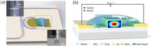
Schematic illustration of the broadband high-efficiency polymerized liquid crystal (LC) metasurfaces with spin-multiplexed functionalities based on wavefront engineering and holographic synthesis. The low-cost LC lenses prepared by photoalignment technology can provide a promising approach for high-throughput nanofabrication, which is of great significance to multifunctional and high-integrity optical systems.