
Jie Zheng, Jinfeng Zhu, Zhilin Yang, "Extremely narrow resonant linewidths in metal-dielectric heterostructures," Photonics Res. 10, 1754 (2022)
- Photonics Research
- Vol. 10, Issue 7, 1754 (2022)
Abstract
1. INTRODUCTION
Plasmonic nanostructures with delicate surface plasmon resonance (SPR) line shapes have been of particular interest in recent years [1–4]. The linewidths refer to the full-width at half-maximum (FWHM) of the resonant peaks/valleys of the plasmonic nanostructures. The narrow SPR linewidths are advantageous for biochemical sensors, nanolasers, and optical imaging. An efficient way to narrow SPR linewidths is to assemble periodic arrays by utilizing diffractive coupling with neighboring particles [5,6]. Crozier’s group demonstrated narrow near-infrared resonance peaks in two-dimensional gold nanoparticle arrays by coupling between grating diffraction and localized surface plasmons [7]. Ren’s group achieved the narrowest linewidth of 3 nm at 960 nm in gold hexagonal arrays [8]. Additionally, in the last few years, a host of strategies or efforts have been devoted to achieving narrower linewidths, including reducing the surface roughness [9], designing the patterns of plasmonic nanostructures [10–12], choosing the materials of the metallic layer [13], and forming bound states in the continuum (BIC) of plasmonic-photonic systems [14–16]. However, extensive attention to narrowing SPR linewidths has mainly focused on noble metal nanostructures, which can support SPR from the visible to the THz wavelength regimes [15,17,18]. To achieve narrow SPR linewidths in the UV wavelength band, our group manufactured stable aluminum (Al) plasmonic arrays and achieved a 14-nm narrow SPR linewidth at about a 400-nm wavelength [19]. The unsatisfactory reality of Al nanostructures is the high level of intrinsic ohmic losses [20]. Recently, dielectric nanostructures with high refractive indices have emerged to be a contender in low losses [21,22]. The integration of metallic nanostructures with dielectric nanostructures is demonstrated to mitigate losses [23]. Fortunately, the cooperative interaction between metal and dielectric nanostructures has given rise to vast and novel optical phenomena for functional photonic devices [24–31]. However, it is one of the major issues in narrowing resonant linewidths based on heterostructures. Here, we put forward an efficient strategy to mitigate the losses in plasmonic nanostructures by integrating dielectric nanostructures with Al nanostructures. The motivation for adopting metal-dielectric heterostructures is because the interaction of a lossy Al plasmonic cavity and a lossless dielectric cavity can reduce the non-radiation loss in the near-infrared regime.
In this work, we experimentally design and manufacture a hybrid plasmonic nanostructure consisting of Al and silicon (Si). The Al can support SPR in a wide spectrum from deep ultraviolet (DUV) to near-infrared (NIR) regions. Despite using a Si semiconductor with an indirect bandgap, Si nanostructures are luminescent and can be integrated into a chip. In addition, Si has a large permittivity (
Generally, the heterostructures of metal-dielectric nanostructures are first fabricated individually and then combined by utilizing sophisticated techniques, such as drop casting and molecule linking [32]. In this article, we propose a straightforward fabrication technology for manufacturing heterostructures that are schematically illustrated in Fig. 1(a). Primarily, photoresist nanohole patterns with a 450-nm periodicity and a 250-nm diameter are fabricated on silicon wafers by utilizing nanoimprint lithography (NIL). The fabrication details can be found in Appendix A. Si nanoholes with 100-nm depths are formed via an inductively coupled plasma (ICP) etching system that utilizes photoresist nanoholes as a mask. Finally, a thin Al film 80-nm-thick covers the surface by TEMD-500 thermal evaporation. The residual photoresist layer acts as a spacer, and the thickness is
Sign up for Photonics Research TOC. Get the latest issue of Photonics Research delivered right to you!Sign up now
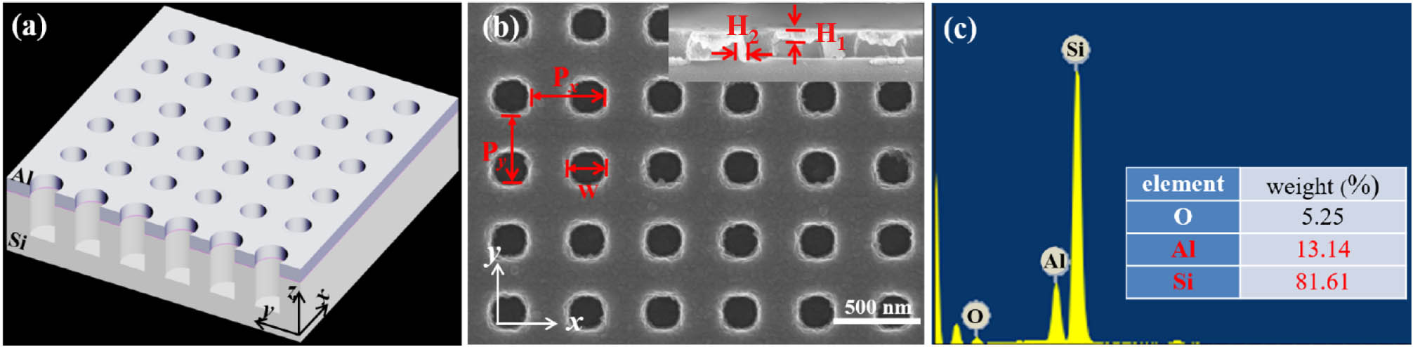
Figure 1.(a) Schematic illustration of the heterostructures. (b) Top-view SEM image of heterostructures, where
2. RESULTS AND DISCUSSION
The Al can support the surface plasmon resonance (SPR) covering from the DUV to NIR regions and is the best candidate for plasmonics in the UV region. However, Al plasmonic nanostructures are restricted by high losses resulting from the difficulty in narrowing resonant linewidths. Fortunately, dielectric nanostructures with low loss can manipulate light at the nanoscale like plasmonic nanostructures. New energies now focus on integrating high-refractive-index dielectric nanostructures and plasmonic nanostructures into the heterostructures to narrow the SPR linewidths. To verify the superiority of introducing Si nanostructures, therein, the reflectance spectra of the Al-Si heterostructures nanoholes are recorded by utilizing a home-built angle-resolved reflectance spectrometer (see Appendix A.2) with varied illumination angles (
![]()
Figure 2.For the spectral analysis, the reflection spectra under different incidence angles and azimuthal angles were collected by the angle-resolved spectrometer. (a) The diagram of the angle-resolved spectrometer, and
Next, we investigate the optical response of the resonant wavelengths and the linewidths of the heterostructures to the varied
Different from the plasmonic nanostructures, which can confine the light in the outside of the nanostructures, the dielectric nanostructures with high indices can concentrate light field into their inside. They manipulate optically induced Mie resonances. To clarify the mechanism of the heterostructures in narrowing the resonant linewidth, the resonant characteristics of the Si nanoholes are analyzed individually. For the scattered field of the Si nanohole arrays in the Cartesian coordinate system, the electric dipole and magnetic dipole can be written as follows [35,36]:
Here,
![]()
Figure 3.Mechanism of Al-Si heterostructures. (a) The resonant modes of the Al nanostructures and the Si nanostructures under varied incidence angles. (b) The energy levels of the Al nanostructures and Si nanostructures. The resonant modes of the Si nanostructures will couple to the
The above results demonstrate a narrowing resonant linewidth of 8 nm by adopting the heterostructures. To further investigate the optical properties of the heterostructures for dedicated applications, we recorded reflectance spectra of the heterostructures by changing
![]()
Figure 4.Polarization-dependent optical properties of the heterostructures with an azimuthal angle of 0° by tuning the incident angles of (a) 30°, (b) 45°, and (c) 75° and with an illumination angle 60° by tuning the azimuthal angles of (d) 60°, (e) 75°, and (f) 90°.
3. CONCLUSION
In summary, we successfully fabricate metal/dielectric heterostructures consisting of the periodic metal arrays (Al) and dielectric nanostructures (Si). By introducing the low-loss Si nanostructures, the resonant band with a linewidth of
Acknowledgment
Acknowledgment. The authors thank Professor Lihua Qian for polishing the essay’s language and Dr. Jingyu Wang and Dr. Peiwen Ren for helpful discussions.
APPENDIX A: METHODS
A photoresist layer TU2-70 with 200 nm thickness was spin-coated on the silicon wafer (Obducat Technologies AB, Sweden). The nanopatterns were replicated from a nickel mold (hole array with 450-nm period and 250-nm hole diameter) to photoresist utilizing the Eitre-6 nanoimprint lithography system (Obducat Technologies AB, Sweden). A thermal nanoimprint on the nickel mold was taken with the intermediate polymer sheet (IPS, Obducat Technologies AB, Sweden) at 150°C with 40 bar (
According to the data from Ref. [
![]()
Figure 5.Imaginary part of the refractive index of the Si material is near zero in the visible and NIR regions.
![]()
Figure 6.(a) The spectral analysis equipment of the angle-resolved spectrometer. (b) The diagram of
![]()
Figure 7.Electromagnetic field distribution using commercial FDTD software. (a) The schematic illustration of heterostructures. (b) The electromagnetic field distribution in the
![]()
Figure 8.Top-view SEM image of the Si nanoholes, where
![]()
Figure 9.Reflectance spectra of the Si nanoholes arrays under varied
![]()
Figure 10.Reflectance spectra of the Si nanoholes arrays under varied
![]()
Figure 11.Top-view SEM image of Al nanoholes, where
![]()
Figure 12.Reflection spectra under different incident angles are collected by the angle-resolved spectrometer when the azimuthal angle equals 0°. The illuminating angle equals (a) 15°, (b) 30°, (c) 45°, and (d) 60°.
References
[1] L. Wen, L. Liang, X. Yang, Z. Liu, B. Li, Q. Chen. Multiband and ultrahigh figure-of-merit nanoplasmonic sensing with direct electrical readout in Au-Si nanojunctions. ACS Nano, 13, 6963-6972(2019).
[2] U. Aslam, V. G. Rao, S. Chavez, S. Linic. Catalytic conversion of solar to chemical energy on plasmonic metal nanostructures. Nat. Catal., 1, 656-665(2018).
[3] C. Ji, K.-T. Lee, T. Xu, J. Zhou, H. J. Park, L. J. Guo. Engineering light at the nanoscale: structural color filters and broadband perfect absorbers. Adv. Opt. Mater., 5, 1700368(2017).
[4] M. Gao, W. Yang, Z. Wang, S. Lin, J. Zhu, Z. Yang. Plasmonic resonance-linewidth shrinkage to boost biosensing. Photon. Res., 8, 1226-1235(2020).
[5] A. K. Yang, A. J. Hryn, M. R. Bourgeois, W.-K. Lee, J. Hu, G. C. Schatz, T. W. Odom. Programmable and reversible plasmon mode engineering. Proc. Natl. Acad. Sci. USA, 113, 14201-14206(2016).
[6] V. G. Kravets, A. V. Kabashin, W. L. Barnes, A. N. Grigorenko. Plasmonic surface lattice resonances: a review of properties and applications. Chem. Rev., 118, 5912-5951(2018).
[7] Y. Chu, E. Schonbrun, T. Yang, K. B. Crozier. Experimental observation of narrow surface plasmon resonances in gold nanoparticle arrays. Appl. Phys. Lett., 93, 181108(2008).
[8] B. Liu, S. Chen, J. Zhang, X. Yao, J. Zhong, H. Lin, T. Huang, Z. Yang, J. Zhu, S. Liu, C. Lienau, L. Wang, B. Ren. A plasmonic sensor array with ultrahigh figures of merit and resonance linewidths down to 3 nm. Adv. Mater., 30, 1706031(2018).
[9] X. Zhu, Y. Zhang, J. Zhang, J. Xu, Y. Ma, Z. Li, D. Yu. Ultrafine and smooth full metal nanostructures for plasmonics. Adv. Mater., 22, 4345-4349(2010).
[10] S. Zhang, G.-C. Li, Y. Chen, X. Zhu, S.-D. Liu, D. Lei, H. Duan. Pronounced Fano resonance in single gold split nanodisks with 15 nm split gaps for intensive second harmonic generation. ACS Nano, 10, 11105-11114(2016).
[11] M. P. Knudson, R. Li, D. Wang, W. Wang, R. D. Schaller, T. W. Odom. Polarization-dependent lasing behavior from low-symmetry nanocavity arrays. ACS Nano, 13, 7435-7441(2019).
[12] M. L. Tseng, J. Yang, M. Semmlinger, C. Zhang, P. Nordlander, N. J. Halas. Two-dimensional active tuning of an aluminum plasmonic array for full-spectrum response. Nano Lett., 17, 6034-6039(2017).
[13] K. V. Sreekanth, Y. Alapan, M. ElKabbash, E. Ilker, M. Hinczewski, U. A. Gurkan, A. D. Luca, G. Strangi. Extreme sensitivity biosensing platform based on hyperbolic metamaterials. Nat. Mater., 15, 621-627(2016).
[14] Y. Liang, K. Koshelev, F. Zhang, H. Lin, S. Lin, J. Wu, B. Jia, Y. Kivshar. Bound states in the continuum in anisotropic plasmonic metasurfaces. Nano Lett., 20, 6351-6356(2020).
[15] Y. Liang, H. Lin, S. Lin, J. Wu, W. Li, F. Meng, Y. Yang, X. Huang, B. Jia, Y. Kivshar. Hybrid anisotropic plasmonic metasurfaces with multiple resonances of focused light beams. Nano Lett., 21, 8917-8923(2021).
[16] S. I. Azzam, V. M. Shalaev, A. Boltasseva, A. V. Kildishev. Formation of bound states in the continuum in hybrid plasmonic-photonic systems. Phys. Rev. Lett., 121, 253901(2018).
[17] M. S. Bin-Alam, O. Reshef, Y. Mamchur, M. Z. Alam, G. Carlow, J. Upham, B. T. Sullivan, J.-M. Ménard, M. J. Huttunen, R. W. Boyd, K. Dolgaleva. Ultra-high-
[18] N. J. J. van Hoof, D. R. Abujetas, S. E. T. ter Huurne, F. Verdelli, G. C. A. Timmermans, J. A. Sánchez-Gil, J. G. Rivas. Unveiling the symmetry protection of bound states in the continuum with terahertz near-field imaging. ACS Photon., 8, 3010-3016(2021).
[19] J. Zheng, W. Yang, J. Wang, J. Zhu, L. Qian, Z. Yang. An ultranarrow SPR linewidth in the UV region for plasmonic sensing. Nanoscale, 11, 4061-4066(2019).
[20] J. B. Khurgin, A. Boltasseva. Reflecting upon the losses in plasmonics and metamaterials. MRS Bull., 37, 768-779(2012).
[21] A. I. Kuznetsov, A. E. Miroshnichenko, M. L. Brongersma, Y. S. Kivshar, B. Luk’yanchuk. Optically resonant dielectric nanostructures. Science, 354, aag2472(2016).
[22] K. Koshelev, Y. Kivshar. Dielectric resonant metaphotonics. ACS Photon., 8, 102-112(2021).
[23] Y. Yang, O. D. Miller, T. Christensen, J. D. Joannopoulos, M. Soljačić. Low-loss plasmonic dielectric nanoresonators. Nano Lett., 17, 3238-3245(2017).
[24] C. Wei, Y. S. Zhao. Photonic applications of metal–dielectric heterostructured nanomaterials. ACS Appl. Mater. Interfaces, 8, 3703-3713(2016).
[25] M. Achermann. Exciton–plasmon interactions in metal–semiconductor nanostructures. J. Phys. Chem. Lett., 1, 2837-2843(2010).
[26] Y. Q. Qu, X. F. Duan. Progress, challenge and perspective of heterogeneous photocatalysts. Chem. Soc. Rev., 42, 2568-2580(2013).
[27] R. Jiang, B. Li, C. Fang, J. Wang. Metal/semiconductor hybrid nanostructures for plasmon enhanced applications. Adv. Mater., 26, 5274-5309(2014).
[28] S. K. Dutta, S. K. Mehetor, N. Pradhan. Metal semiconductor heterostructures for photocatalytic conversion of light energy. J. Phys. Chem. Lett., 6, 936-944(2015).
[29] C. Jia, X. Li, N. Xin, Y. Gong, J. Guan, L. Meng, S. Meng, X. Guo. Interface-engineered plasmonics in metal/semiconductor heterostructures. Adv. Energy Mater., 6, 1600431(2016).
[30] X.-C. Ma, Y. Dai, L. Yu, B.-B. Huang. Energy transfer in plasmonic photocatalytic composites. Light Sci. Appl., 5, e16017(2016).
[31] A. I. Barreda, M. Zapata-Herrera, I. M. Palstra, L. Mercadé, J. Aizpurua, A. F. Koenderink, A. Martínez. Hybrid photonic-plasmonic cavities based on the nanoparticle-on-a-mirror configuration. Photon. Res., 9, 2398-2419(2021).
[32] X. X. Han, W. Ji, B. Zhao, Y. Ozaki. Semiconductor-enhanced Raman scattering: active nanomaterials and applications. Nanoscale, 9, 4847-4861(2017).
[33] M. Gao, Y. He, Y. Chen, T.-M. Shih, W. Yang, J. Wang, F. Zhao, M.-D. Li, H. Chen, Z. Yang. Tunable surface plasmon polaritons and ultrafast dynamics in 2D nanohole arrays. Nanoscale, 11, 16428-16436(2019).
[34] K. Yang, J. Wang, X. Yao, D. Lyu, J. Zhu, Z. Yang, B. Liu, B. Ren. Large-area plasmonic metamaterial with thickness-dependent absorption. Adv. Opt. Mater., 9, 2001375(2021).
[35] T. Liu, R. Xu, P. Yu, Z. Wang, J. Takahara. Multipole and multimode engineering in Mie resonance-based metastructures. Nanophotonics, 9, 1115-1137(2020).
[36] A. B. Evlyukhin, C. Reinhardt, B. N. Chichkov. Multipole light scattering by nonspherical nanoparticles in the discrete dipole approximation. Phys. Rev. B, 84, 235429(2011).
[37] E. Cao, W. Lin, M. Sun, W. Liang, Y. Song. Exciton-plasmon coupling interactions: from principle to applications. Nanophotonics, 7, 145-167(2018).
[38] C. Schinke, P. C. Peest, J. Schmidt, R. Brendel, K. Bothe, M. R. Vogt, I. Kröger, S. Winter, A. Schirmacher, S. Lim, H. T. Nguyen, D. MacDonald. Uncertainty analysis for the coefficient of band-to-band absorption of crystalline silicon. AIP Adv., 5, 067168(2015).


Set citation alerts for the article
Please enter your email address

© Copyright 2018-2021 | Chinese Laser Press. All Rights Reserved 沪ICP备15018463号-20