
Yongduck Jung, Daniel Burt, Lin Zhang, Youngmin Kim, Hyo-Jun Joo, Melvina Chen, Simone Assali, Oussama Moutanabbir, Chuan Seng Tan, Donguk Nam. Optically pumped low-threshold microdisk lasers on a GeSn-on-insulator substrate with reduced defect density[J]. Photonics Research, 2022, 10(6): 1332
- Photonics Research
- Vol. 10, Issue 6, 1332 (2022)
Abstract
1. INTRODUCTION
The demonstration of Ge lasers [1,2] has opened new opportunities towards realizing complementary metal–oxide–semiconductor (CMOS)-compatible light sources on silicon (Si). During the last few years, a great amount of effort has been put into lowering the lasing threshold and increasing the operating temperature of Ge-based lasers for practical applications. Major routes that most researchers have investigated to improve the performance of Ge-based lasers are to employ tensile strain engineering [3–18] and Sn alloying [19–32]. Both approaches can increase the directness of Ge, thereby making the material suitable for high-performance on-chip lasers, which hold the key to monolithic integration of photonic-integrated circuits [33–35].
While material quality also plays a significant role in determining the performance of laser devices [36], it has not been extensively studied how the defects in the lasing gain medium influence the performance of GeSn lasers. Most of the previously reported GeSn lasers used epitaxially grown GeSn layers, which have a significant number of interfacial defects due to the lattice mismatch between the GeSn and Ge buffer layers [31]. Recently, a 10-fold improvement in the lasing threshold of GeSn microdisks was obtained by removing the defective GeSn–Ge interface using a reactive ion etching [24]. Because gas has a lower etching selectivity of GeSn over the Ge compared to the gas, which is commonly used for a selective dry etch of the Ge layer, etching chemistry was employed to remove the defective interface. However, the selective etch applied in this study allows removing defects only at the locally exposed region of the suspended microdisk. This suspended structure inherently has poor thermal conduction due to the underlying air gap, thus increasing the lasing threshold [18–24].
In this work, we experimentally demonstrate that the reduced defect density in high-quality GeSn-on-insulator (GeSnOI) microdisk lasers can reduce the lasing threshold by times compared to the same microdisk lasers made in as-grown GeSn-on-Si (GeSnOS). The GeSnOI substrate achieved a globally removed defective interfacial layer between GeSn and Ge by employing a chemical–mechanical polishing (CMP) process. Additionally, improved thermal conduction was achieved by releasing GeSn microdisks to the underlying oxide layer while simultaneously relaxing the harmful compressive strain, which is detrimental to lasing performance. The GeSnOI microdisk lasers show clear lasing behaviors at a threshold of , which is 6.4 times lower than the threshold of the microdisk lasers directly fabricated on an as-grown GeSnOS () substrate. Our results provide a new possibility to improve the performance of GeSn lasers by employing a high Sn content CMOS-compatible GeSnOI substrate with a significantly reduced defect density.
Sign up for Photonics Research TOC. Get the latest issue of Photonics Research delivered right to you!Sign up now
2. SUBSTRATE FABRICATION AND OPTICAL CHARACTERIZATION
Figures 1(a) and 1(b) show cross-sectional TEM images of the as-grown GeSnOS and GeSnOI substrates. In the GeSnOS sample, a 960-nm-thick GeSn epilayer with a Sn content of 8% (atomic fraction) was grown on a 150-mm Si wafer with a 1-μm-thick Ge buffer layer using reduced pressure chemical vapor deposition (RPCVD) at 250°C. The compressive GeSn epilayer becomes relaxed as it grows thicker, which allows for a larger amount of Sn atoms to be incorporated into the lattice. As a result, the GeSn layer at the surface obtains a Sn content of 10.4%. A large plastic relaxation occurs during the GeSn epitaxial growth due to the lattice mismatch between the Ge buffer layer and GeSn epilayer, resulting in a large number of misfit dislocations at the interface between the layers. Misfit dislocations are visible at GeSn–Ge and Ge–Si interfaces that form during growth as a result of the large lattice mismatch between the two layers [Fig. 1(a)]. The highly defective interface will result in enhanced non-radiative recombination, shortening the minority carrier lifetime and degrading the material’s internal quantum efficiency (IQE), in turn increasing the lasing threshold [36,37]. To overcome this issue, the GeSnOI substrate was fabricated using a low-temperature () direct bonding process to prevent Sn segregation [32]. The same GeSn layer with the defective interface was used as a carrier wafer to produce the GeSnOI substrate. The carrier wafer is diced into carrier chips. A thermal oxide layer with a thickness of was grown on a 150-mm handle Si, which was also diced into handle chips. Then a 180-nm-thick amorphous aluminum oxide () layer was deposited on both carrier and handle chips by atomic layer deposition (ALD). Next, the CMP process was employed to reduce the surface roughness of both layers to less than 0.2 nm, which is crucial for strong direct bonding. Subsequently, both chips underwent cleaning processes, followed by plasma exposure to further activate the surface [38]. Deionized water rinsing was carried out to increase the surface hydroxyl coverage on the layers, resulting in stronger interfacial bonding between the carrier and handle chips, and a nitrogen gun was used to remove the remaining water on both chips. The direct bonding was carried out by flipping the carrier chip upside down and bringing the carrier and handle chip surfaces into contact followed by post bonding annealing at 225°C for 3 h in an ambient gas. After direct bonding, the highly defective interface is located on top of the GeSn layer. The Si substrate of the carrier chip was thinned down to a thickness of 50 μm by mechanical grinding, followed by potassium hydroxide (KOH) wet etching to selectively remove the remaining Si. After direct bonding and the removal of the Si carrier chip, the top surface region of the substrate contains the defects produced during the GeSn epitaxial growth. A final CMP process was conducted to effectively polish away the 1-μm-thick Ge buffer layer and GeSn layer containing the highly defective interface, resulting in a high-quality GeSnOI layer with a thickness of 910 nm [Fig. 1(b)].
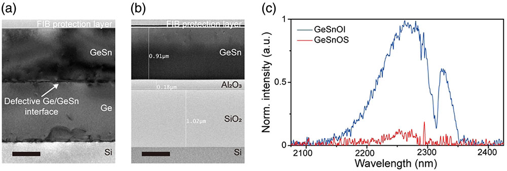
Figure 1.(a), (b) Cross-sectional TEM images of (a) GeSnOS and (b) GeSnOI substrates. Scale bar, 500 nm. (c) PL spectra from GeSnOI and GeSnOS substrates. The measurement temperature is 4 K.
To compare the optical emission of the GeSnOI and GeSnOS substrates, low-temperature photoluminescence (PL) measurements were conducted at 4 K. The samples were excited with a 532-nm continuous-wave (CW) laser with a fixed pump power density of , and the optical emission was sent to a Fourier transform infrared (FTIR) spectrometer equipped with an extended InGaAs detector. A times increase in PL intensity was achieved from the GeSnOI substrate compared to the GeSnOS sample, as shown in Fig. 1(c). It should be noted that the dips in intensity near are caused by an FTIR artifact and do not originate from the samples. An observed shift of in the emission of the GeSnOI substrate is due to the slightly relaxed compressive strain in the GeSn layer as a result of the bonding process [39]. To understand the origin of this enhanced emission, we must consider the effect of the defect-assisted recombination lifetime on IQE. The IQE can be defined as the ratio of the radiative recombination rate to the sum of the radiative and non-radiative recombination rates [36]. When non-radiative recombination dominates radiative recombination, even a small improvement in the defect density will substantially improve the IQE [36]. Thus, the reduction in the defect density in our GeSnOI sample is particularly effective in improving the light-emitting efficiency of GeSn, which currently has a very low IQE of [40].
3. DEVICE FABRICATION AND SIMULATIONS
To study the effect of the defective interface on lasing performance, microdisk cavities were fabricated using both the GeSnOI and GeSnOS substrates. The 8-μm-diameter microdisks were patterned by photolithography, followed by anisotropic reactive ion etching (RIE) to transfer the pattern. For the GeSnOI microdisks, tetramethylammonium hydroxide (TMAH) wet etching was followed to remove the sacrificial layer, producing GeSn microdisks sitting directly on the underlying [Fig. 2(a)]. For the GeSnOS microdisks, the Ge buffer layer was selectively removed by isotropic RIE, making the GeSn microdisk collapse onto underlying Si. Both microdisks were stuck to the underlying layer, allowing for achieving superior thermal conduction, unlike conventional suspended structures. During the undercut process, the limiting compressive strain in both microdisks is relaxed. Figure 2(b) shows a scanning electron microscopy (SEM) image of a typical fabricated microdisk laser structure on GeSnOI.
![]()
Figure 2.(a) Schematic illustration of the microdisk structure fabrication process. (b) Tilted-view SEM image of GeSnOI microdisk. Scale bar, 2 μm.
To ensure the defective interface is the predominant variable influencing the lasing characteristics of the two samples, other variables should be carefully eliminated. To confirm the effect of the different underlying layers ( for GeSnOI and Si for GeSnOS) on the optical confinement and thermal conduction, finite-difference time-domain (FDTD) and finite element method (FEM) simulations were conducted. The simulation results confirmed that optical Q-factors and thermal conduction for both the GeSnOI and GeSnOS microdisks are nearly identical as shown in Fig. 3. The FDTD simulation results show a slightly higher Q-factor of GeSnOI microdisks () compared to that of GeSnOS microdisks (), which can be attributed to the relatively large difference in refractive index between GeSn and . For the FEM simulation, the ambient temperature, pulse width, and pulse repetition rate of optical pumping were set to 4 K, 5 ns, and 1 MHz, respectively (matching the conditions used for the lasing measurements). The thermal conductivity of GeSn was set to , which is lower than that of Ge, because Sn interstitials significantly decrease the thermal conductivity of GeSn alloy [41]. The FEM simulation results show the difference in the temperature is only as shown in Figs. 3(e) and 3(f). Therefore, the heating effects are negligible for both GeSnOS and GeSnOI microdisks. As a result of both FDTD and FEM simulations, the Q-factor and thermal conduction can be treated as negligible variables, leaving the presence of a defective interface as the only key variable for comparison of the lasing characteristics between the two substrates.
![]()
Figure 3.(a), (b) Top views of simulated electric field distributions in the (a) GeSnOI and (b) GeSnOS microdisk structures, which achieve high-quality factors of
4. OPTICAL CHARACTERIZATION
Figures 4(a) and 4(b) present the 4 K PL spectra of both GeSnOI and GeSnOS microdisks at different pump powers. A pulsed laser pumping at 1550 nm was used with a pulse width and repetition rate of 5 ns and 1 MHz, respectively. While both microdisks show the emergence of sharp lasing peaks as the pump power is increased, lasing in the GeSnOI microdisk occurs at a much lower pump power density compared to the GeSnOS microdisk. The improved threshold for the GeSnOI microdisk can be also appreciated in Figs. 4(c) and 4(d), which show double-logarithmic (main) and linear (inset) light-in-light-out (L-L) curves of GeSnOI and GeSnOS microdisks, respectively. Clear threshold behaviors of both GeSnOI and GeSnOS microdisks were observed from the non-linear S-shaped behavior in the log–log plots, which is a hallmark of lasing action. The lasing thresholds for GeSnOI and GeSnOS are and , respectively. The lasing threshold of the GeSnOI microdisk is approximately 6.4 times lower than that of the GeSnOS microdisk. The reduced threshold for GeSnOI can be mainly attributed to the removal of the defective interface since the difference in the heating between the two samples is negligible. A theoretical work previously explained the significance of the non-radiative recombination lifetime in reducing the threshold of Ge-based lasers [36]. The reduced defect density in GeSnOI can lead to an increased non-radiative recombination lifetime and an improved IQE, resulting in the reduced lasing threshold. Figures 4(e) and 4(f) show the full width at half-maximum (FWHM) of the lasing peaks. A significant reduction in the FWHM of the lasing peaks below 1 nm at the lasing threshold is another clear evidence of lasing. The maximum lasing operating temperature of the GeSnOI microdisk was 90 K (not shown here).
![]()
Figure 4.(a), (b) PL spectra from (a) GeSnOI and (b) GeSnOS microdisks at different pump powers. (c), (d) Double-logarithmic L-L curves for (c) GeSnOI and (d) GeSnOS microdisks. Insets: linear L-L curves. (e), (f) FWHMs for (e) GeSnOI and (f) GeSnOS microdisks at different pump powers.
5. CONCLUSION
In summary, we have experimentally demonstrated that removing the Ge–GeSn defective interface in GeSn can drastically improve the lasing performance. By using a low-temperature direct bonding technique and CMP process, we obtained a high-quality GeSnOI substrate with the global removal of the defective interfaces introduced during the epitaxial growth. We confirmed that the defective interfaces were successfully removed by the CMP process by using cross-sectional TEM of GeSnOI and GeSnOS substrates. The removal of the defective interface resulted in an increased PL intensity by times. To study the effect of the defective interface on the lasing threshold, we fabricated GeSnOI and GeSnOS microdisk lasers. Both microdisks were stuck to the underlying layer using a selective etch, allowing us to simultaneously achieve good thermal conduction and relax the limiting compressive strain in GeSn. By carefully designing PL experiments with all other variables well controlled, we studied the effect of a defective interface on the lasing threshold. We achieved a lasing threshold power density of in the GeSnOI microdisk, which is 6.4 times lower than the GeSnOS microdisk containing the defective interface. Our work emphasizes the importance of defect management to push the performance of GeSn lasers to the limit. Our demonstration also suggests a scalable route towards obtaining high-quality GeSn gain media by presenting a low-temperature direct bonding technique to obtain GeSnOI with high Sn contents.
Acknowledgment
Acknowledgment. The authors thank Nanyang NanoFabrication Centre (N2FC) for assistance in the GeSn substrates and microdisks fabrication.
References
[1] J. Liu, X. Sun, R. Camacho-Aguilera, L. C. Kimerling, J. Michel. Ge-on-Si laser operating at room temperature. Opt. Lett., 35, 679-681(2010).
[2] R. Koerner, M. Oehme, M. Gollhofer, M. Schmid, K. Kostecki, S. Bechler, D. Widmann, E. Kasper, J. Schulze. Electrically pumped lasing from Ge Fabry-Perot resonators on Si. Opt. Express, 23, 14815-14822(2015).
[3] D. Nam, D. Sukhdeo, A. Roy, K. Balram, S.-L. Cheng, K. C.-Y. Huang, Z. Yuan, M. Brongersma, Y. Nishi, D. Miller, K. Saraswat. Strained germanium thin film membrane on silicon substrate for optoelectronics. Opt. Express, 19, 25866-25872(2011).
[4] A. Elbaz, M. Kurdi, A. Aassime, S. Sauvage, X. Checoury, I. Sagnes, C. Baudot, F. Boeuf, P. Boucaud. Germanium microlasers on metallic pedestals. APL Photon., 3, 106102(2018).
[5] D. Nam, D. Sukhdeo, J.-H. Kang, J. Petykiewicz, J. H. Lee, W. Jung, J. Vučković, M. Brongersma, K. Saraswat. Strain-induced pseudoheterostructure nanowires confining carriers at room temperature with nanoscale-tunable band profiles. Nano Lett., 13, 3118-3123(2013).
[6] K. Guilloy, N. Pauc, A. Gassenq, Y.-M. Niquet, J.-M. Escalante, I. Duchemin, S. Tardif, G. O. Dias, D. Rouchon, J. Widiez, J.-M. Hartmann, R. Geiger, T. Zabel, H. Sigg, J. Faist, A. Chelnokov, V. Reboud. Germanium under high tensile stress: nonlinear dependence of direct band gap vs strain. ACS Photon., 3, 1907-1911(2016).
[7] J. Petykiewicz, D. Nam, D. Sukhdeo, S. Gupta, S. Buckley, A. Y. Piggott, J. Vučković, K. Saraswat. Direct bandgap light emission from strained germanium nanowires coupled with high-
[8] D. A. Smith, V. C. Holmberg, B. A. Korgel. Flexible germanium nanowires: ideal strength, room temperature plasticity, and bendable semiconductor fabric. ACS Nano, 4, 2356(2010).
[9] D. S. Sukhdeo, D. Nam, J.-H. Kang, M. L. Brongersma, K. C. Saraswat. Direct bandgap germanium-on-silicon inferred from 5.7% ⟨100⟩ uniaxial tensile strain. Photon. Res., 2, A8-A13(2014).
[10] Y. Ishikawa, K. Wada, D. D. Cannon, J. Liu, H. C. Luan, L. C. Kimerling. Strain-induced band gap shrinkage in Ge grown on Si substrate. Appl. Phys. Lett., 82, 2044-2046(2003).
[11] Z. Qi, H. Sun, M. Luo, Y. Jung, D. Nam. Strained germanium nanowire optoelectronic devices for photonic-integrated circuits. J. Phys. Condens. Matter, 30, 334004(2018).
[12] A. Ghrib, M. El Kurdi, M. de Kersauson, M. Prost, S. Sauvage, X. Checoury, G. Beaudoin, I. Sagnes, P. Boucaud. Tensile-strained germanium microdisks. Appl. Phys. Lett., 102, 221112(2013).
[13] Y. Jung, Y. Kim, D. Burt, H.-J. Joo, D.-H. Kang, M. Luo, M. Chen, L. Zhang, C. S. Tan, D. Nam. Biaxially strained germanium crossbeam with a high-quality optical cavity for on-chip laser applications. Opt. Express, 29, 14174-14181(2021).
[14] M. de Kersauson, M. El Kurdi, S. David, X. Checoury, G. Fishman, S. Sauvage, R. Jakomin, G. Beaudoin, I. Sagnes, P. Boucaud. Optical gain in single tensile-strained germanium photonic wire. Opt. Express, 19, 17925-17934(2011).
[15] S. Bao, D. Kim, C. Onwukaeme, S. Gupta, K. Saraswat, K. H. Lee, Y. Kim, D. Min, Y. Jung, H. Qiu, H. Wang, E. A. Fitzgerald, C. S. Tan, D. Nam. Low-threshold optically pumped lasing in highly strained germanium nanowires. Nat. Commun., 8, 1845(2017).
[16] M. J. Süess, R. Geiger, R. A. Minamisawa, G. Schiefler, J. Frigerio, D. Chrastina, G. Isella, R. Spolenak, J. Faist, H. Sigg. Analysis of enhanced light emission from highly strained germanium microbridges. Nat. Photonics, 7, 466-472(2013).
[17] D. Nam, D. S. Sukhdeo, S. Gupta, J. H. Kang, M. L. Brongersma, K. C. Saraswat. Study of carrier statistics in uniaxially strained Ge for a low-threshold Ge laser. IEEE J. Sel. Top. Quantum Electron., 20, 1500107(2014).
[18] F. T. A. Pilon, A. Lyasota, Y.-M. Niquet, V. Reboud, V. Calvo, N. Pauc, J. Widiez, C. Bonzon, J. M. Hartmann, A. Chelnokov, J. Faist, H. Sigg. Lasing in strained germanium microbridges. Nat. Commun., 10, 2724(2019).
[19] Q. M. Thai, N. Pauc, J. Aubin, M. Bertrand, J. Chrétien, V. Delaye, A. Chelnokov, J.-M. Hartmann, V. Reboud, V. Calvo. GeSn heterostructure micro-disk laser operating at 230 K. Opt. Express, 26, 32500-32508(2018).
[20] J. Chrétien, N. Pauc, F. A. Pilon, M. Bertrand, Q.-M. Thai, L. Casiez, N. Bernier, H. Dansas, P. Gergaud, E. Delamadeleine, R. Khazaka, H. Sigg, J. Faist, A. Chelnokov, V. Reboud, J.-M. Hartmann, V. Calvo. GeSn lasers covering a wide wavelength range thanks to uniaxial tensile strain. ACS Photon., 6, 2462-2469(2019).
[21] D. Stange, S. Wirths, R. Geiger, C. Schulte-Braucks, B. Marzban, N. von den Driesch, G. Mussler, T. Zabel, T. Stoica, J.-M. Hartmann, S. Mantl, Z. Ikonic, D. Grützmacher, H. Sigg, J. Witzens, D. Buca. Optically pumped GeSn microdisk lasers on Si. ACS Photon., 3, 1279-1285(2016).
[22] Y. Kim, S. Assali, D. Burt, Y. Jung, H.-J. Joo, M. Chen, Z. Ikonic, O. Moutanabbir, D. Nam. Enhanced GeSn microdisk lasers directly released on Si. Adv. Opt. Mater., 10, 2101213(2021).
[23] A. Elbaz, D. Buca, N. von den Driesch, K. Pantzas, G. Patriarche, N. Zerounian, E. Herth, X. Checoury, S. Sauvage, I. Sagnes, A. Foti, R. Ossikovski, J.-M. Hartmann, F. Boeuf, Z. Ikonic, P. Boucaud, D. Grützmacher, M. El Kurdi. Ultra-low-threshold continuous-wave and pulsed lasing in tensile-strained GeSn alloys. Nat. Photonics, 14, 375-382(2020).
[24] A. Elbaz, R. Arefin, E. Sakat, B. Wang, E. Herth, G. Patriarche, A. Foti, R. Ossikovski, S. Sauvage, X. Checoury, K. Pantzas, I. Sagnes, J. Chrétien, L. Casiez, M. Bertrand, V. Calvo, N. Pauc, A. Chelnokov, P. Boucaud, F. Boeuf, V. Reboud, J.-M. Hartmann, M. El Kurdi. Reduced lasing thresholds in GeSn microdisk cavities with defect management of the optically active region. ACS Photon., 7, 2713-2722(2020).
[25] H. Joo, Y. Kim, D. Burt, Y. Jung, L. Zhang, M. Chen, S. J. Parluhutan, D.-H. Kang, C. Lee, S. Assali, Z. Ikonic, O. Moutanabbir, Y.-H. Cho, C. S. Tan, D. Nam. 1D photonic crystal direct bandgap GeSn-on-insulator laser. Appl. Phys. Lett., 119, 201101(2021).
[26] S. Wirths, R. Geiger, N. von den Driesch, G. Mussler, T. Stoica, S. Mantl, Z. Ikonic, M. Luysberg, S. Chiussi, J. M. Hartmann, H. Sigg, J. Faist, D. Buca, D. Grützmacher. Lasing in direct-bandgap GeSn alloy grown on Si. Nat. Photonics, 9, 88-92(2015).
[27] Y. Zhou, W. Dou, W. Du, S. Ojo, H. Tran, S. A. Ghetmiri, J. Liu, G. Sun, R. Soref, J. Margetis, J. Tolle, B. Li, Z. Chen, M. Mortazavi, S.-Q. Yu. Optically pumped GeSn lasers operating at 270 K with broad waveguide structures on Si. ACS Photon., 6, 1434-1441(2019).
[28] J. Margetis, S. Al-Kabi, W. Du, W. Dou, Y. Zhou, T. Pham, P. Grant, S. Ghetmiri, A. Mosleh, B. Li, J. Liu, G. Sun, R. Soref, J. Tolle, M. Mortazavi, S.-Q. Yu. Si-based GeSn lasers with wavelength coverage of 2-3 μm and operating temperatures up to 180 K. ACS Photon., 5, 827-833(2018).
[29] V. Reboud, A. Gassenq, N. Pauc, J. Aubin, L. Milord, Q. M. Thai, M. Bertrand, K. Guilloy, D. Rouchon, J. Rothman, T. Zabel, F. A. Pilon, H. Sigg, A. Chelnokov, J. M. Hartmann, V. Calvo. Optically pumped GeSn micro-disks with 16% Sn lasing at 3.1 μm up to 180 K. Appl. Phys. Lett., 111, 092101(2017).
[30] D. Sukhdeo, Y. Kim, S. Gupta, K. Saraswat, B. Dutt, D. Nam. Theoretical modeling for the interaction of tin alloying with n-type doping and tensile strain for GeSn lasers. IEEE Electron Device Lett., 37, 1307-1310(2016).
[31] R. Chen, H. Lin, Y. Huo, C. Hitzman, T. I. Kamins, J. S. Harris. Increased sminescence of strain-reduced, high-Sn composition
[32] D. Burt, H.-J. Joo, Y. Jung, Y. Kim, Y.-C. Huang, D. Nam. Strain-relaxed GeSn-on-insulator (GeSnOI) microdisks. Opt. Express, 29, 28959-28967(2021).
[33] Z. Zhou, B. Yin, J. Michel. On-chip light sources for silicon photonics. Light Sci. Appl., 4, e358(2015).
[34] O. Moutanabbir, S. Assali, X. Gong, E. O’Reilly, C. A. Broderick, B. Marzban, J. Witzens, W. Du, S.-Q. Yu, A. Chelnokov, D. Buca, D. Nam. Monolithic infrared silicon photonics: the rise of (Si)GeSn semiconductors. Appl. Phys. Lett., 118, 110502(2021).
[35] R. Soref. The past, present, and future of silicon photonics. IEEE J. Sel. Top. Quantum Electron., 12, 1678-1687(2006).
[36] D. S. Sukhdeo, S. Gupta, K. C. Saraswat, B. Dutt, D. Nam. Impact of minority carrier lifetime on the performance of strained germanium light sources. Opt. Commun., 364, 233-237(2016).
[37] D. Nam, J.-H. Kang, M. L. Brongersma, K. C. Saraswat. Observation of improved minority carrier lifetimes in high-quality Ge-on-insulator using time-resolved photoluminescence. Opt. Lett., 39, 6205-6208(2014).
[38] G. Y. Chong, C. S. Tan. Low temperature PE-TEOS oxide bonding assisted by a thin layer of
[39] D. Lei, K. H. Lee, S. Bao, W. Wang, B. Wang, X. Gong, C. S. Tan, Y.-C. Yeo. GeSn-on-insulator substrate formed by direct wafer bonding. Appl. Phys. Lett., 109, 022106(2016).
[40] Q. Zhang, Y. Liu, G. Han, Y. Shao, X. Gao, C. Zhang, J. Zhang, Y. Hao. Theoretical analysis of performance enhancement in GeSn/SiGeSn light-emitting diode enabled by Si3N4 liner stressor technique. Appl. Opt., 55, 9668-9674(2016).
[41] N. Uchida, T. Maeda, R. R. Lieten, S. Okajima, Y. Ohishi, R. Takase, M. Ishimaru, J.-P. Locquet. Carrier and heat transport properties of polycrystalline GeSn films on SiO2. Appl. Phys. Lett., 107, 232105(2015).

Set citation alerts for the article
Please enter your email address
© Copyright 2018-2021 | Chinese Laser Press. All Rights Reserved 沪ICP备15018463号-20