
Shangsen Sun, Zhiqiang Yang, Juanli Wang, Runsen Zhang, Fengchun Zhang, Ning Zhu, Lei Wan, Zhaohui Li, "Ultra-sharp silicon multimode waveguide bends based on double free-form curves," Photonics Res. 10, 1484 (2022)
- Photonics Research
- Vol. 10, Issue 6, 1484 (2022)
Abstract
1. INTRODUCTION
With the development of all kinds of data services, information technology is now facing an extreme challenge in requirements for the expansion of transmission capacity accommodated within a single optical fiber [1–5]. The newly proposed mode-division multiplexing (MDM) technology utilizes different modes in the same wavelength band, and the amount of carried information can be further increased by this method [6–9]. In order to compactly route the guided modes in the on-chip multimode communication system, many functional waveguide devices suitable for multimode manipulations have been reported, including tapers [10,11], mode converters [12,13], multimode waveguide crossings [14–17], and multimode waveguide bends (MWBs) [12,18]. It is well known that when the transmitted light passes through a conventional MWB with compact size, there will be serious inter-couplings between the original guided modes inside the straight waveguide and the distorted modes inside the bent waveguide [19], causing unignorable excess losses and inter-modal crosstalks. Besides, for all kinds of the multimode waveguides, higher order modes have weak optical field confinement and tend to require a larger bending radius to reduce the radiation losses. An optimized waveguide bend requires a larger bending radius to accommodate more modes. Therefore, the design of a bent waveguide with a small radius and supporting as many modes as possible is of great significance to the monolithic MDM system [20].
In recent years, many methods have been proposed to realize the sharp bending of on-chip silicon multimode waveguides. An ultra-sharp silicon MWB based on the meta-surface (grating-like) structures has been proposed. The nonuniform grating mode converter on the straight multimode waveguide converts the “straight modes” to the “bent modes” ahead of the bend by changing the effective refractive index of the straight waveguide [21]. By this method a subwavelength grating (SWG) waveguide supporting four modes is achieved with the effective radius of 45.8 μm. Alternatively, these SWG structures can be also used to compensate for the structural asymmetry in the sharp bending region and convert the “bent modes” back to “straight modes” in the bent waveguide. The proposed MWB with the SWG on the bending part can support four TE modes with a bending radius of only 20 μm [22]. However, the manufacturing processes of these SWG-assisted bends are rather complex, which raises the scattering loss as well as the cost to some extent. Using a specially designed curve as the bending part of an MWB is another way to reduce the effective radius, since a curve with gradually changing radius can greatly reduce the mode field mismatch at the waveguide junction. MWBs based on the Bezier curve supporting three TE modes and on the modified Euler curve supporting four TM modes are designed, with bending radii of 20 μm and 45 μm, respectively [23,24]. Although these kinds of devices usually provide better transmission efficiencies by avoiding the scattering from the subwavelength mode-converting structures, the sizes are limited by the mathematical functions of the curves. While all the designs mentioned above use arc or other curves to bend the light, total internal reflection (TIR) can also be utilized to redirect the light [25]. Based on this principle, multimode waveguide corner bend (MWCB) supporting up to 10 TE modes is reported with the effective radius of 35 μm. Unfortunately, the MWCB requires a long adiabatic taper, which potentially deteriorates the integration density of the device. Other design methods of MWBs such as using mode converters and Etalon lens have also been proposed, but the scalability to higher order modes may be the key problem limiting the applications of these methods [12,18].
Instead of solving the problems forward, some works based at least partially on inverse design methods have also been proposed. An MWB supporting four TE modes with an effective radius of 17 μm is presented with the help of the transformation optics (TO) method [26]. The TO method is to map the traditional waveguide bend in the physical space to the virtual space as a distorted graded index waveguide. The boundary shape of this distorted waveguide in the virtual space is inversely optimized for highly efficient multimode transmission by the quadratic approximation method, and is then mapped back to the physical space to acquire the final sharp bending with high performance. In our previous work, an ultra-compact 90° MWB based on the inverse design has also been proposed [27]. The special curve in this work optimized by the inverse design method is called the free-form curve. The curve is directly optimized for multimode transmission in the physical space. The proposed free-form curve is such a smooth curve that the curvature radius of every point on it can be defined freely without the constraint of any mathematical function, and it is set to be self-symmetric around the angular bisector for convenience. In practice it is discretized by a series of different arcs (the discretization number is
Sign up for Photonics Research TOC. Get the latest issue of Photonics Research delivered right to you!Sign up now
2. DESIGN AND SIMULATIONS
As shown in Fig. 1, the MWB with an equivalent radius of 10 μm is composed of two free-form curves A and B.
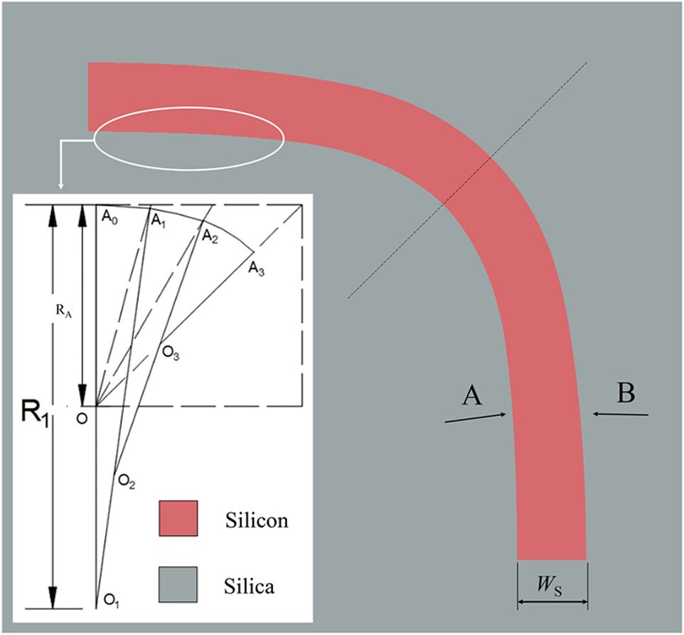
Figure 1.Proposed MWB based on the DFFC design. DFFC consists of curve A and curve B, and
It is well known that setting some reasonable initial parameters is very important and time-saving for the inverse design [39,40]. In our previous work,
After curve A and curve B are obtained from Eq. (2), the width at the narrowest point of MWB is used as a screening criterion. Waveguides failing to support all the required modes with too small width at the narrowest point will be discarded. After comparing the values of the FOM, 100 groups of DFFCs with available performance are found. The segment radii normalized by the effective bending radius are shown in Fig. 2. At the following stage, the curves A and B will be reversely designed using the DRS algorithm described in Ref. [27]. In short, the optimization process can be defined as follows. Each
![]()
Figure 2.Proper combinations of (a) curve A and (b) curve B are given. Here the ordinate represents a multiple of the equivalent radius.
![]()
Figure 3.Simulation results of the DFFC–MWB with an input width
![]()
Figure 4.Simulation results of the DFFC–MWB with an input width
In order to demonstrate the superiority of the DFFC design on the SFFC design in our previous work, an MWB based on the SFFC with the same effective radius and waveguide width is also simulated. The results are compared with each other in Table 1. For simplicity, only the worst cases of all crosstalk values at 1.55 μm are displayed in the table. It should be noted that these crosstalk values do not necessarily come from the same mode. As shown in Table 1, it is obvious that the performances of the DFFC designs are more balanced and better than those of the SFFC ones. The excess losses and crosstalks of the DFFC–MWBs are better than those of the SFFC–MWBs for almost all modes. Only the loss for the
Last but not least, the fabrication tolerance should also be taken into account when selecting different MWB designs. For electron-beam lithography (EBL), the main fabrication error of an MWB device arises from the width deviation caused by the proximity effect in the exposure. In Fig. 5, we give the effects from the width deviation on the excess loss and crosstalk of a four-mode MWB. Since the deviation is much smaller than the waveguide width, we set the deviation
![]()
Figure 5.Transmittance spectra of the MWB based on the DFFC with
3. FABRICATION AND CHARACTERIZATION
The devices fabricated on the SOI platform are tested to verify the above simulation results. The thickness of the silicon core layer and the silica under cladding layer is 0.22 and 2 μm, respectively. The EBL is used to define the patterns, and inductively coupled plasma (ICP) dry etching is applied to transfer the patterns to the silicon core layer. The mode (de)multiplexers with four mode channels are composed of asymmetrical directional couplers (ADCs) to (de)multiplex all the required modes [21,27]. The
![]()
Figure 6.Microscopic view of the fabricated silicon multimode bends with four mode channels. The multiplexer and demultiplexer are connected with (a) straight multimode waveguide or (b) eight cascaded 90° MWBs based on the DFFC. (c) SEM image of the cascaded MWBs.
A tunable laser (Keysight 8164B) is used as well as a high-speed photodiode (Agilent 11982A) to measure the transmittance spectra of the fabricated devices. The insertion losses of the mode (de)multiplexers and the vertical grating couplers should be extracted from the transmission curve of each MWB [as shown in Figs. 6(a) and 6(b)]. The measured spectra of a single 90° four-mode bend based on the DFFC are shown in Figs. 7(a)–7(d). For the
![]()
Figure 7.Measured spectra of the normalized transmittances of a single four-mode waveguide bend. (a)–(h) Measurement results of a single 90° four-mode bend based on (a)–(d) DFFC or (e)–(h) SFFC.
Table 2 shows the comparison between the previously reported MWBs based on different structures and this work. It is obvious that both for the three-mode and four-mode MWBs, this work has better overall performance. To support the same number of TE modes, the MWBs based on the DFFC are almost half the size of those based on the SWGs [22]. The equivalent radius of the proposed device allowing high transmittance of three TE modes is only 6 μm, which is already close to the radius of the silicon single mode waveguide bend, and that of the MWB with four-mode transmission is only 10 μm, which is the smallest four-mode bend to the best of our knowledge.
Comparison of the Reported Results of Silicon Multimode Waveguide Bends
| Reference | Method | EL (dB) | CT (dB) | ||||
|---|---|---|---|---|---|---|---|
| Theory | Meas. | Theory | Meas. | ||||
| [ | SWG tapers | 4 | 45.8 | 0.4 | 1 | −20 | −20 |
| [ | SWGs | 3 | 10 | 0.5 | 0.7 | −30 | −20 |
| 4 | 20 | 0.5 | 0.8 | −26 | −15 | ||
| [ | Euler curves | 4 | 45 | 0.1 | 0.5 | −25 | −20 |
| [ | Bezier curves | 3 | 20 | 0.2 | / | −26 | −23 |
| [ | Corner bend | 2 | 7 | 0.18 | 0.53 | −36 | −15 |
| 10 | 35 | 0.54 | / | −24 | / | ||
| [ | TO-optimized | 4 | 17 | 0.1 | 0.55 | −20 | −17 |
| [ | SFFC | 3 | 9.35 | 0.04 | 0.2 | −29 | −25 |
| This work | DFFC | 3 | 6 | 0.17 | / | −31 | / |
| 4 | 10 | 0.13 | 0.72 | −29 | −25 | ||
SWG, subwavelength grating; TO, transformation optics; SFFC, single free-form curve; DFFC, double free-form curve; EL, excess loss; CT, crosstalk;
4. CONCLUSION
In this paper, we have proposed and demonstrated an MWB based on the DFFC. The improved DRS algorithm is used to optimize the shape of the DFFC. Unlike the Bezier curve or other mathematical functions, the DFFC utilizes two curves for which the changing of the segment radius is free instead of constraining in a certain mathematical form. The MWBs with effective radii of 6 μm and 10 μm are designed to support three modes and four modes, respectively. Theoretically, the bending losses of the three-mode MWB are calculated to be 0.008, 0.013, and 0.175 dB at 1.55 μm, for the
References
[1] L. Liu, Y. Ding, K. Yvind, J. M. Hvam. Silicon-on-insulator polarization splitting and rotating device for polarization diversity circuits. Opt. Express, 19, 12646-12651(2011).
[2] R. Chen, K. W. Ng, W. S. Ko, D. Parekh, F. Lu, T. Tran, K. Li, C. Chang-Hasnain. Nanophotonic integrated circuits from nanoresonators grown on silicon. Nat. Commun., 5, 4325(2014).
[3] L. W. Luo, N. Ophir, C. P. Chen, L. H. Gabrielli, M. Lipson. WDM-compatible mode-division multiplexing on a silicon chip. Nat. Commun., 5, 3069(2014).
[4] P. J. Winzer. Making spatial multiplexing a reality. Nat. Photonics, 8, 345-348(2014).
[5] L.-T. Feng, M. Zhang, Z.-Y. Zhou, M. Li, X. Xiong, L. Yu, B.-S. Shi, G.-P. Guo, D.-X. Dai, X.-F. Ren. On-chip coherent conversion of photonic quantum entanglement between different degrees of freedom. Nat. Commun., 7, 11985(2016).
[6] D. Dai, J. Wang, Y. Shi. Silicon mode (de)multiplexer enabling high capacity photonic networks-on-chip with a single-wavelength-carrier light. Opt. Lett., 38, 1422-1424(2013).
[7] D. Dai, J. Wang, S. Chen, S. Wang, S. He. Monolithically integrated 64-channel silicon hybrid demultiplexer enabling simultaneous wavelength- and mode-division-multiplexing. Laser Photon. Rev., 9, 339-344(2015).
[8] G. Chen, Y. Yu, X. Zhang. Monolithically mode division multiplexing photonic integrated circuit for large-capacity optical interconnection. Opt. Lett., 41, 3543-3546(2016).
[9] J. Chen, Y. Yang, N. Zhu. Echelle grating based mode demultipexer for vertical mode-division multiplexing. Opt. Express, 24, 24509-24516(2016).
[10] S. H. Badri, M. Gilarlue. Ultrashort waveguide tapers based on Luneburg lens. J. Opt., 21, 125802(2019).
[11] L. Sun, R. Zhang. Metamaterial-based ultrashort multimode waveguide taper with low intermodal crosstalk. Opt. Express, 29, 7124-7133(2021).
[12] S. H. Badri, H. R. Saghai, H. Soofi. Polymer multimode waveguide bend based on a multilayered Eaton lens. Appl. Opt., 58, 5219-5224(2019).
[13] H. Jia, H. Chen, T. Wang, H. Xiao, G. Ren, A. Mitchell, J. Yang, Y. Tian. Multi-channel parallel silicon mode-order converter for multimode on-chip optical switching. IEEE J. Sel. Top. Quantum Electron., 26, 8302106(2019).
[14] W. Chang, L. Lu, X. Ren, D. Li, Z. Pan, M. Cheng, D. Liu, M. Zhang. Ultra compact dual-mode waveguide crossing based on subwavelength multimode-interference couplers. Photon. Res., 6, 660-665(2018).
[15] S. Li, Y. Zhou, J. Dong, X. Zhang, E. Cassan, J. Hou, C. Yang, S. Chen, D. Gao, H. Chen. Universal multimode waveguide crossing based on transformation optics. Optica, 5, 1549-1556(2018).
[16] W. Chang, L. Lu, X. Ren, L. Lu, M. Cheng, D. Liu, M. Zhang. An ultra compact multimode waveguide crossing based on subwavelength asymmetric Y-junction. IEEE Photon. J., 10, 4501008(2018).
[17] S. H. Badri, H. R. Saghai, H. Soofi. Polygonal Maxwell’s fisheye lens via transformation optics as multimode waveguide crossing. J. Opt., 21, 065102(2019).
[18] C. Sun, Y. Yu, G. Chen, X. Zhang. Ultra-compact bent multimode silicon waveguide with ultralow inter-mode crosstalk. Opt. Lett., 42, 3004-3007(2017).
[19] L. H. Gabrielli, D. Liu, S. G. Johnson, M. Lipson. On-chip transformation optics for multimode waveguide bends. Nat. Commun., 3, 1217(2012).
[20] L. Yang, T. Zhou, H. Jia, S. Yang, J. Ding, X. Fu, L. Zhang. General architectures for on-chip optical space and mode switching. Optica, 5, 180-187(2018).
[21] H. Xu, Y. Shi. Ultra-sharp multi-mode waveguide bending assisted with metamaterial-based mode converters. Laser Photon. Rev., 12, 1700240(2018).
[22] H. Wu, C. Li, L. Song, H. K. Tsang, J. E. Bowers, D. Dai. Ultra-sharp multimode waveguide bends with subwavelength gratings. Laser Photon. Rev., 13, 1800119(2019).
[23] X. Jiang, W. Hao, D. Dai. Low-loss and low-crosstalk multimode waveguide bend on silicon. Opt. Express, 26, 17680-17689(2018).
[24] X. Wu, W. Zhou, D. Huang, Z. Zhang, Y. Wang, J. Bowers, H. K. Tsang. Low crosstalk bent multimode waveguide for on-chip mode-division multiplexing interconnects. CLEO: QELS_Fundamental Science, JW2A.66(2018).
[25] Y. Wang, D. Dai. Multimode silicon photonic waveguide corner-bend. Opt. Express, 28, 9062-9071(2020).
[26] S. Li, L. Cai, D. Gao, J. Dong, J. Hou, C. Yang, S. Chen, X. Zhang. Compact and broadband multimode waveguide bend by shape-optimizing with transformation optics. Photon. Res., 8, 1843-1849(2020).
[27] S. Sun, P. Dong, F. Zhang, J. Wang, N. Zhu, Y. Shi. Inverse design of ultra-compact multimode waveguide bends based on the free‐form curves. Laser Photon. Rev., 15, 2100162(2021).
[28] S. Kirpatrick, C. D. Gelatt, M. P. Vecchi. Optimization by simulated annealing. Readings in Computer Vision, 606-615(1987).
[29] A. Rickman. The commercialization of silicon photonics. Nat. Photonics, 8, 579-582(2014).
[30] H.-L. Han, H. Li, X.-P. Zhang, A. Liu, T.-Y. Lin, Z. Chen, H.-B. Lv, M.-H. Lu, X.-P. Liu, Y.-F. Chen. High performance ultra-compact SOI waveguide crossing. Opt. Express, 26, 25602-25610(2018).
[31] S. Molesky, Z. Lin, A. Y. Piggott, W. Jin, J. Vucković, A. W. Rodriguez. Inverse design in nanophotonics. Nat. Photonics, 12, 659-670(2018).
[32] Y. Liu, K. Xu, S. Wang, W. Shen, H. Xie, Y. Wang, S. Xiao, Y. Yao, J. Du, Z. He. Arbitrarily routed mode-division multiplexed photonic circuits for dense integration. Nat. Commun., 10, 3263(2019).
[33] Z. Liu, X. Liu, Z. Xiao, C. Lu, H.-Q. Wang, Y. Wu, X. Hu, Y.-C. Liu, H. Zhang, X. Zhang. Integrated nanophotonic wavelength router based on an intelligent algorithm. Optica, 6, 1367-1373(2019).
[34] K. Yao, R. Unni, Y. Zheng. Intelligent nanophotonics: merging photonics and artificial intelligence at the nanoscale. Nanophotonics, 8, 339-366(2019).
[35] Y. Augenstein, C. Rockstuhl. Inverse design of nanophotonic devices with structural integrity. ACS Photon., 7, 2190-2196(2020).
[36] M. A. Seldowitz, J. P. Allebach, D. W. Sweeney. Synthesis of digital holograms by direct binary search. Appl. Opt., 26, 2788-2798(1987).
[37] M. Hochberg, T. Baehr-Jones. Towards fabless silicon photonics. Nat. Photonics, 4, 492-494(2010).
[38] N. Hoppe, T. Föhn, P. Diersing, P. Scheck, W. Vogel, M. F. Rosa, M. Kaschel, M. Bach, M. Berroth. Design of an integrated dual-mode interferometer on 250 nm silicon-on-insulator. IEEE J. Sel. Top. Quantum Electron., 23, 444-451(2016).
[39] B. Shen, P. Wang, R. Polson, R. Menon. An integrated-nanophotonics polarization beamsplitter with 2.4 × 2.4 μm2 footprint. Nat. Photonics, 9, 378-382(2015).
[40] A. Y. Piggott, J. Lu, K. G. Lagoudakis, J. Petykiewicz, T. M. Babinec, J. Vučković. Inverse design and demonstration of a compact and broadband on-chip wavelength demultiplexer. Nat. Photonics, 9, 374-377(2015).


Set citation alerts for the article
Please enter your email address

© Copyright 2018-2021 | Chinese Laser Press. All Rights Reserved 沪ICP备15018463号-20