
Zicheng Song, Pingping Min, Jiaqi Zhu, Lei Yang, Feng Han Lin, "Wideband diffusion metabsorber for perfect scattering field reduction," Photonics Res. 10, 1361 (2022)
- Photonics Research
- Vol. 10, Issue 6, 1361 (2022)
Abstract
1. INTRODUCTION
Along with the development of the electromagnetic (EM) industry, 5th generation mobile communication brings unlimited possibilities for low-latency and high-speed applications, but also increases unwanted EM radiation, risking public health and the stability of electronic systems [1–4]. EM protection has become an urgent need for the area around radiation sources such as airport control towers or communication base stations, thereby requiring the EM shielding window. With aid of transparent conductive film, optical windows can effectively reflect incident EM waves. However, the secondary pollution caused by backward scattering energy concentration presents a new challenge for window design.
With the blossom of micro-nano processing, the concept of a metasurface is proposed for arbitrary control of EM waves, providing an effective method for microwave scattering field reduction [5–7]. Also, transparent resistive films and dielectrics are extended for low microwave scattering transparent metasurface design [8–10]. Hence a series of window-use metasurfaces are proposed for reducing microwave reflection, which can be divided into metasurface absorbers (metabsorbers) and diffusion metasurfaces according to the different principles.
Absorbers dissipate incident EM wave energy into heat energy, and the introduction of metasurface design further improves bandwidth [11–15], thickness [16,17], flexibility [18–22], and angular tolerance [23–25]. As an alternative scheme, diffusion metasurfaces diffuse EM waves by destructive interference using anti-phase reflection elements [26–30]. As a combination of both, diffusion metabsorbers (DMAs) have the potential to further reduce a scattering field by simultaneously dissipating and diffusing EM wave using anti-phase absorptive elements [31,32]. Although some valuable attempts have been made to arrange a set of anti-phase absorptive elements in a rectangular grid with specific distribution, the scattering field reduction of those designs is not significantly improved or is only narrowband [33–36]; this is because their elements have narrow absorption bands and little overlap among them. The difficulty in designing wideband absorptive anti-phase reflection elements hinders further improvement in scattering field reduction for DMAs.
Sign up for Photonics Research TOC. Get the latest issue of Photonics Research delivered right to you!Sign up now
In this study, we proposed a wideband DMA that simultaneously absorbs and diffuses wideband EM waves. With aid of the wideband characteristic of a bilateral design, two elements are proposed with low-amplitude and anti-phase reflection. For proof of concept, the proposed absorptive elements with anti-phase reflection are arranged in a rectangular grid. The scattering fields of an element array are calculated by field vector addition, and thereby the distribution of elements can be optimized by a genetic algorithm (GA) aiming for reflection reduction. The proposed DMA achieves over 20-dB backward scattering field reduction from 8.5 to 20.3 GHz, and angular stability of up to 40° under both TE and TM polarization waves incidence, which is verified through experiment. All simulations are performed in the CST Studio Suite 2020 [37]. The simultaneous application of wideband absorption and the diffusion principle pave the path for achieving perfect scattering field reduction for optical window application.
2. DESIGN AND SIMULATION
Inspired by continuous mode resonance of complementary metabsorbers generating wideband absorption [14,15], the DMA basic element is designed and shown in Fig. 1. Complementary gammadion-shaped resonators are placed in the top two layers, with a reflection layer at the bottom. Air gaps are sandwiched by the layers made of indium tin oxide (ITO)–polyethylene terephthalate (PET) film [
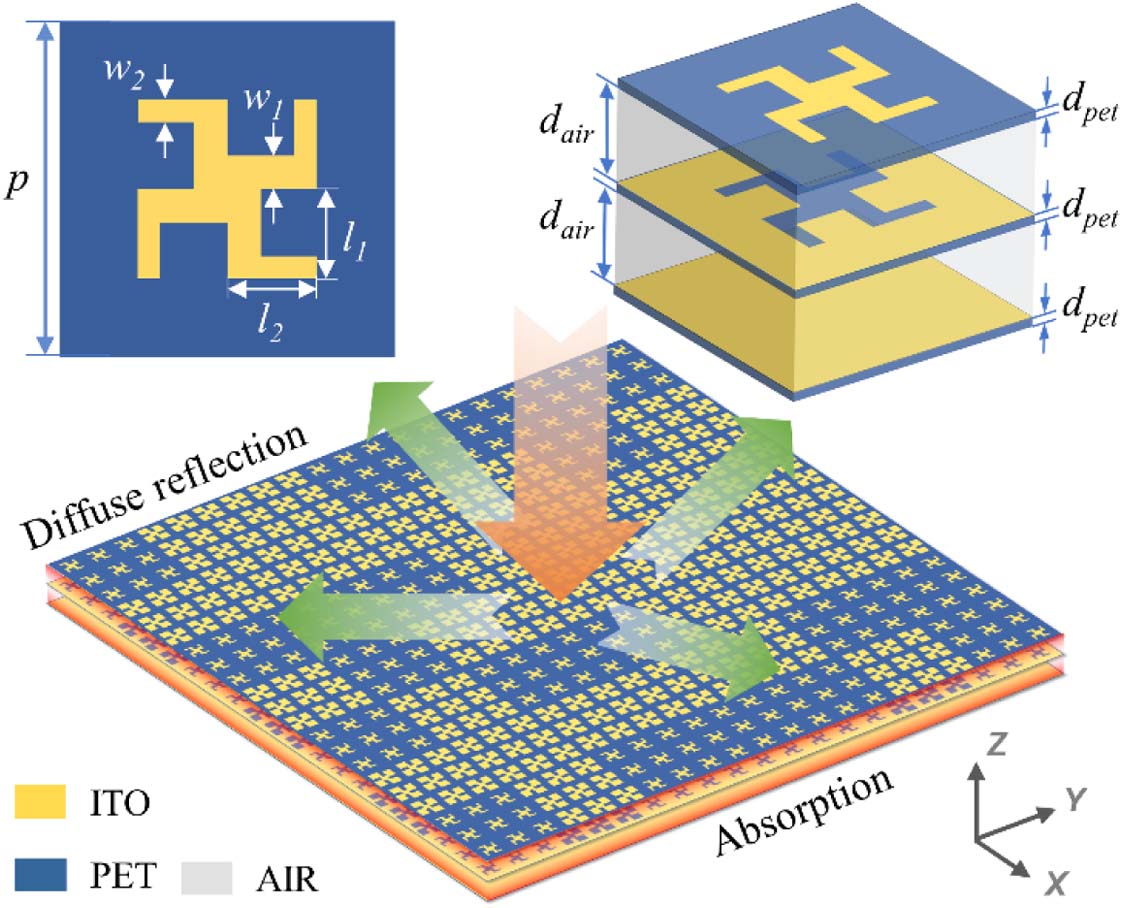
Figure 1.Geometric structure of metabsorber element and schematic of wideband diffusion metabsorber under normal incidence.
To qualitatively reveal the absorption performance of the proposed DMA elements, the influence of the key structural parameters for the gammadion-shaped resonator is studied. As can be seen in Fig. 2, the absorption of the element is insensitive to parameters
![]()
Figure 2.Effect of changing structural parameters on absorption. (a) Length of gammadion-shaped resonator inner arm. (b) Length of gammadion-shaped resonator outer arm. (c) Width of gammadion-shaped resonator inner arm. (d) Width of gammadion-shaped resonator outer arm.
By properly adjusting the parameters of the resonator, anti-phase elements 1 and 2 are designed and shown in Fig. 3, whose parameters are
![]()
Figure 3.Simulated (a) reflection amplitude and (b) reflection phase of optimized elements. The normalized input impedance of (c) elements 1 and (d) element 2. Insets shows thumbnails of elements.
For proof of concept, a DMA containing
![]()
Figure 4.(a) Element distribution for optimized diffusion metabsorber. (b) Scattering field reduction results of calculation and simulation. (c) Ratio of absorption, diffusion, and reflection under normal incidence. (d) Averaged ratio of absorption, diffusion, and reflection from 8.5 to 20.3 GHz, and proportion of diffusion and reflection to the total scattered energy.
To provide insight into the field reduction effectiveness of the optimized structure, the proposed structure under normal plane wave irradiation is simulated, whose scenario is shown in Fig. 1. As shown in Fig. 4(b), DMA reduces dominant scattering over 20 dB in the range of 8.5–20.3 GHz, with the relative bandwidth greater than 80%. Moreover, the calculated result using field vector addition fits the full-wave simulation result well, indicating the correctness of the calculation. The slight drop in simulated result between 12 and 17 GHz might be caused by the difference in the boundary between the periodical elements and the actual array.
To analyze the role of absorption and diffuse reflection in scattering reduction, the ratio of absorption, reflection (broadside direction), and diffusion (other directions) energy under normal incidence is given in Fig. 4(c), denoted by different colors. Due to the good conductivity of the ground layer, the transmission energy is extremely low (
To further analyze the spatial scattering field distribution of DMA, calculated and full-wave simulated scattering field patterns are compared at 10,14 and 18 GHz. Notably, the scattering fields of the proposed DMA are normalized with respect to the PEC plate of the same size, as shown in Figs. 5(a)–5(f). As can be seen, calculated and simulated three-dimensional far-field patterns of DMA for each frequency exhibit similar spatial distribution, indicating the field vector addition results fit full-wave simulation results well.
![]()
Figure 5.(a)–(c) Calculated scattering patterns and full-wave simulated scattering field patterns for (d)–(f) optimized diffusion metabsorber and (g)–(i) PEC plate at frequencies of 10, 14, and 18 GHz.
Although a boundary difference causes the difference among minor lobes, it does not affect the optimization results aiming at major lobes with dominant energy. Furthermore, DMA effectively diffuses incidence waves among the entire backward space, which is shown by a comparison of the reflection response between DMA and the PEC plate in Figs. 5(d)–5(i). The incidence wave is effectively reflected by the PEC plate concentrated on the broadside. Compared with the typical pencil-beam pattern of a PEC plate, the main lobe of DMA is split into several lobes, leading to power flow dispersed to all backward space as diffusion-like reflection, so that only 16.8% of the total scattered energy is reflected to the normal direction as shown in Fig. 4(d). Most of the incident wave is dissipated by the induced current flowing on the resistive film. Therefore, DMA simultaneously dissipates and diffuses the incidence wave, leading to the effectively reduced scattering field in backward spatial space.
To quantitatively analyze the reduction effectiveness of the proposed structure, the E-plane and H-plane scattering patterns of DMA and the PEC plate are compared in Fig. 6. With aid of simultaneous absorption and diffusion, DMA exhibits over 20-dB reduction of the scattering field in 0° direction, which is consistent with calculation results shown in Fig. 4(b). Moreover, the scattering field of DMA represented by the green line is surrounded by the scattering field of the PEC plate represented by the orange line, indicating the scattering field of the proposed structure reduces in the entire backward space. Due to the absorption of anti-phase elements, the scattering field is not only homogenized in a larger spatial space but also reduced by dissipation, which leads to the near-omnidirectional scattering field reduction.
![]()
Figure 6.Simulated scattering field at (a)–(c)
For practical applications, the polarization stability and angular stability of the proposed structure are evaluated. Notably, to better express the reduction of a spatial scattering field, the maximum scattering field of DMA and the PEC plate of the E-field are selected to generate normalized scattering reduction when the plane wave has normal or oblique incidence. Figure 7 indicates that DMA maintains a wideband 20-dB reduction in the range of 8.5–20.3 GHz with the increase in polarization angle when the plane wave has normal incidence. With aid of a four-fold symmetric design of the elements, the proposed structure exhibits excellent polarization stability, although the elements are randomly arranged. Furthermore, the reduction performance of DMA under TE and TM polarization wave oblique incidence is shown in Fig. 8. Under both wave irradiations, the scattering reduction is maintained over 20 dB at the incident angle from 0° to 20°, while the bandwidth remains nearly unchanged. Along with the increase in incident angle up to 40°, the 20-dB reduction band slowly shifts to a higher frequency, and the 10-dB reduction band covers part of the original operation band. Overall, the reduction spectra of TE and TM waves indicate that the proposed design has good scattering reduction performance, covering the entire X- and Ku-bands.
![]()
Figure 7.Simulated scattering field reduction of proposed diffusion metabsorber versus frequency and polarization angle (
![]()
Figure 8.Simulated scattering field reduction of proposed diffusion metabsorber under oblique incidences of (a) TE and (b) TM polarization waves.
3. FABRICATION AND CHARACTERIZATION
To verify the wideband anti-reflection characteristic, a proposed structure with a size of
![]()
Figure 9.(a) Photograph of the fabricated sample and normalized reflection spectra of the proposed sample at different incident angles: (b) 3° (normal incidence), (c) 20°, and (d) 40°. Inset in (b) shows the configuration of the arch method for reflection characterization.
The anti-reflection performance of the sample is characterized through the arch method, whose configuration is shown in the inset of Fig. 9(b). Wideband linearly polarized horn antennas on the arc frame are connected to a vector network analyzer to measure the reflection of the sample, which is normalized with a metal plate of the same size. As shown in Fig. 9(b), the measured reflection of the sample is lower than 0.1 at 6–21 GHz under normal incidence, confirming the wideband anti-reflection performance of the proposed sample. By symmetrically changing the position of the transmitter and receiver antennas on the arc frame, the reflection results of samples at 20° and 40° incident angles for TE and TM waves are depicted in Figs. 9(c) and 9(d). The measured reflection is less than 0.1 from 6 to 18 GHz, which verifies the field reduction performance in a wide range of incident angles. The measured and simulated results are in good agreement, and the slight difference is due to the insertion of PMMA frames and the deviation of the material parameters and experimental system. Overall, the experiment results validate the scattering field reduction of the proposed DMA, thereby demonstrating the effectiveness of the wideband anti-reflection design strategy.
4. CONCLUSION
In this work, we proposed a wideband DMA achieving more than 20-dB scattering field reduction in the range of 8.5–20.3 GHz. With aid of the wideband absorption characteristic of complementary resonator design, the reflection amplitude and phase of elements can be regulated independently, hence providing an effective strategy to generate wideband anti-phase absorption elements. By optimizing the distribution of elements, the proposed DMA exhibits wideband perfect scattering field reduction utilizing simultaneous absorption and diffusion. Moreover, the proposed design strategy and sample with excellent polarization and angular stability have great potential for EM scattering energy reduction applications.
Acknowledgment
Acknowledgment. We gratefully acknowledge Dr. Yixuan Zhang from Xidian University for the discussion on the method of field vector addition.
References
[1] N. Seyhan. Electromagnetic pollution and our health. Noro Psikiyatr Ars., 47, 158-161(2010).
[2] O. Genc, M. Bayrak, E. Yaldiz. Analysis of the effects of GSM frequency band to electromagnetic pollution in the RF spectrum. Prog. Electromagn. Res., 101, 17-32(2010).
[3] M. A. A. Frah, V. V. Belyaev. Parameters of electromagnetic pollution from different sources and their hazard impact. J. Phys. Conf. Ser., 1309, 012013(2019).
[4] A. Lerchl. Electromagnetic pollution: another risk factor for infertility, or a red herring?. Asian J. Androl., 15, 201-203(2013).
[5] P. Su, Y. Zhao, S. Jia, W. Shi, H. Wang. An ultra-wideband and polarization-independent metasurfaces for RCS reduction. Sci. Rep., 6, 20387(2016).
[6] W. Li, T. Wu, W. Wang, P. Zhai, J. Guan. Broadband patterned magnetic microwave absorber. J. Appl. Phys., 116, 044110(2014).
[7] M. Moccia, S. Liu, R. Y. Wu, G. Castaldi, A. Andreone, T. J. Cui, V. Galdi. Coding metasurfaces for diffuse scattering: scaling laws, bounds, and suboptimal design. Adv. Opt. Mater., 5, 1700455(2017).
[8] Y. Okano, S. Ogino, K. Ishikawa. Development of optically transparent ultrathin microwave absorber for ultrahigh-frequency RF identification system. IEEE Trans. Microw. Theory Tech., 60, 2456-2464(2012).
[9] C. Zhang, Q. Cheng, J. Yang, J. Zhao, T. J. Cui. Broadband metamaterial for optical transparency and microwave absorption. Appl. Phys. Lett., 110, 143511(2017).
[10] H. Sheokand, S. Ghosh, G. Singh, M. Saikia, K. V. Srivastava, J. Ramkumar, S. A. Ramakrishna. Transparent broadband metamaterial absorber based on resistive films. J. Appl. Phys., 122, 105105(2017).
[11] Y. Wu, H. Lin, J. Xiong, J. Hou, R. Zhou, F. Deng, R. Tang. A broadband metamaterial absorber design using characteristic modes analysis. J. Appl. Phys., 129, 134902(2021).
[12] Y. Chen, K. Chen, D. Zhang, S. Li, Y. Xu, X. Wang, S. Zhuang. Ultrabroadband microwave absorber based on 3D water microchannels. Photon. Res., 9, 1391-1396(2021).
[13] Z. Yao, S. Xiao, Y. Li, B. Wang. On the design of wideband absorber based on multilayer and multiresonant FSS array. IEEE Antennas Wireless Propag. Lett., 20, 284-288(2021).
[14] Z. Song, J. Zhu, L. Yang, P. Min, F. H. Lin. Wideband metasurface absorber (metabsorber) using characteristic mode analysis. Opt. Express, 29, 35387-35399(2021).
[15] Z. Song, P. Min, L. Yang, J. Zhu, F. H. Lin. A bilateral coding metabsorber using characteristic mode analysis. IEEE Antennas Wireless Propag. Lett..
[16] S. Lai, Y. Wu, X. Zhu, W. Gu, W. Wu. An optically transparent ultrabroadband microwave absorber. IEEE Photon. J., 9, 5503310(2017).
[17] Z. Song, P. Min, L. Yang, J. Zhu. High optical transparent wideband microwave absorber. IEEE International Conference on Electronic Information and Communication Technology (ICEICT), 391-393(2021).
[18] K. Batrakov, P. Kuzhir, S. Maksimenko, A. Paddubskaya, S. Voronovich, P. Lambin, T. Kaplas, Y. Svirko. Flexible transparent graphene/polymer multilayers for efficient electromagnetic field absorption. Sci. Rep., 4, 7191(2014).
[19] R. Deng, K. Zhang, M. Li, L. Song, T. Zhang. Targeted design, analysis and experimental characterization offlexible microwave absorber for window application. Mater. Des., 162, 119-129(2019).
[20] T. Jang, H. Youn, Y. J. Shin, L. J. Guo. Transparent and flexible polarization-independent microwave broadband absorber. ACS Photon., 1, 279-284(2014).
[21] P. Min, Z. Song, L. Yang, V. G. Ralchenko, J. Zhu. Optically transparent flexible broadband metamaterial absorber based on topology optimization design. Micromachines, 12, 1419(2021).
[22] C. Zhang, J. Yang, W. Cao, W. Yuan, J. Ke, L. Yang, Q. Cheng, T. J. Cui. Transparently curved metamaterial with broadband millimeter wave absorption. Photon. Res., 7, 478-485(2019).
[23] D. Hu, J. Cao, W. Li, C. Zhang, T. Wu, Q. Li, Z. Chen, Y. Wang, J. Guan. Optically transparent broadband microwave absorbing metamaterial for standing-up closed-loop resonators. Adv. Opt. Mater., 5, 1700109(2017).
[24] Y. Shen, J. Zhang, Y. Pang, J. Wang, H. Ma, S. Qu. Transparent broadband metamaterial absorber enhanced by water-substrate incorporation. Opt. Express, 26, 15665-15674(2018).
[25] P. Min, Z. Song, L. Yang, B. Dai, J. Zhu. Transparent ultrawideband absorber based on simple patterned resistive metasurface with three resonant modes. Opt. Express, 28, 19518-19530(2020).
[26] C. Zhang, X. Y. Cao, J. Gao, S. J. Li, H. H. Yang, T. Li. Realization of entire-space electromagnetic wave manipulation with multifunctional metasurface. AIP Adv., 9, 015322(2019).
[27] W. Chen, C. A. Balanis, C. R. Birtcher. Checkerboard EBG surfaces for wideband radar cross section reduction. IEEE Trans. Antennas Propag., 63, 2636-2645(2015).
[28] J. Zhao, Q. Cheng, T. Q. Wang, W. Yuan, T. J. Cui. Fast design of broadband terahertz diffusion metasurfaces. Opt. Express, 25, 1050-1061(2017).
[29] K. Chen, W. Guo, G. Ding, J. Zhao, T. Jiang, Y. Feng. Binary geometric phase metasurface for ultra-wideband microwave diffuse scatterings with optical transparency. Opt. Express, 28, 12638-12649(2020).
[30] F. Costa, A. Monorchio, G. Manara. Wideband scattering and diffusion by using diffraction of periodic surfaces and optimized cell geometries. Sci. Rep., 6, 25458(2016).
[31] J. Zhao, C. Zhang, Q. Cheng, J. Yang, T. J. Cui. An optically transparent metasurface for broadband microwave antireflection. Appl. Phys. Lett., 112, 073504(2018).
[32] L. Bao, Q. Ma, G. D. Bai, H. B. Jing, R. Y. Wu, X. Fu, C. Yang, J. Wu, T. J. Cui. Design of digital coding metasurfaces with independent controls of phase and amplitude responses. Appl. Phys. Lett., 113, 063502(2018).
[33] T. Li, K. Chen, G. Ding, J. Zhao, T. Jiang, Y. Feng. Optically transparent metasurface Salisbury screen with wideband microwave absorption. Opt. Express, 26, 34384-34395(2018).
[34] C. Ji, C. Huang, X. Zhang, J. Yang, J. Song, X. Luo. Broadband low-scattering metasurface using a combination of phase cancellation and absorption mechanisms. Opt. Express, 27, 23368-23377(2019).
[35] J. Zhao, B. Sima, N. Jia, C. Wang, B. Zhu, T. Jiang, Y. Feng. Achieving flexible low-scattering metasurface based on randomly distribution of meta-elements. Opt. Express, 24, 27849-27857(2016).
[36] K. Chen, L. Cui, Y. Feng, J. Zhao, T. Jiang, B. Zhu. Coding metasurface for broadband microwave scattering reduction with optical transparency. Opt. Express, 25, 5571-5579(2017).
[37] https://www.cst.com. https://www.cst.com
[38] J. M. Johnson, Y. Rahmat-Samii. Genetic algorithms in engineering electromagnetics. IEEE Antennas Propag. Mag., 39, 7-25(1997).
[39] D. S. Weile, E. Michielssen. Genetic algorithm optimization applied to electromagnetics: a review. IEEE Trans. Antennas Propag., 45, 343-353(1997).
[40] T. J. Cui, S. Liu, L. L. Li. Information entropy of coding metasurface. Light Sci. Appl., 5, e16172(2016).
[41] C. A. Balanis. Antenna Theory: Analysis and Design(2016).
[42] A. D. Brown. Electronically Scanned Arrays MATLAB® Modeling and Simulation(2012).


Set citation alerts for the article
Please enter your email address

© Copyright 2018-2021 | Chinese Laser Press. All Rights Reserved 沪ICP备15018463号-20