
Emma Geisler, Maxime Lecompère, Olivier Soppera, "3D printing of optical materials by processes based on photopolymerization: materials, technologies, and recent advances," Photonics Res. 10, 1344 (2022)
- Photonics Research
- Vol. 10, Issue 6, 1344 (2022)
Abstract
1. INTRODUCTION
3D printing or additive manufacturing (AM), in contrast to subtractive manufacturing, is the process of manufacturing parts in 3D by successively adding material with reference to a 3D model. 3D printing technologies have progressed considerably over the last ten years, from proof-of-concept devices developed in research laboratories to applications in several industrial sectors [1]. The dental industry is a major example, having widely adopted industrial 3D printing of dental structures. Other sectors as diverse as the aerospace [2], the automotive [3], the medical [4] and the food industries [5] also use these technologies.
Numerous types of processes have been developed for 3D printing using various materials, such as metals, ceramics, polymers, and hydrides. Furthermore, several limitations, including object size, resolution, (multi)materials, and complexity, have been overcome. These processes have even enabled the production of geometries unachievable by conventional processes. Moreover, manufacturing using computer-assisted design (CAD) permits better customization and reduced wastage, making it a green technology. These properties are important in 3D manufacturing for optical applications since optical objects are typically manufactured using multi-stage subtractive processes. These require complex machines, generate considerable loss of raw materials, and have limited recyclability.
Among all the materials suitable for optical applications, polymers are prioritized for their advantageous properties: transparency in the visible and infrared range, light weight, adaptable mechanical properties, and adjustable refractive index. Furthermore, additional functionalities such as color, saturable absorption, and luminescence can be imparted to them by simple doping of the polymer matrix. In addition, different processes can be used to structure them, which enables the production of customized objects for diffractive, refractive, and guided optics, such as surface gratings [6,7], lenses, or waveguides [8]. Moreover, different specific optical properties such as birefringence and photochromism can be acquired. Transparent materials with a tunable refractive index [9,10], photoactive materials with a varying refractive index [11], and Bragg gratings [12] are all examples of materials with specific optical properties.
Sign up for Photonics Research TOC. Get the latest issue of Photonics Research delivered right to you!Sign up now
By exploiting the liquid state of polymers in different forms, optical objects can be manufactured using either rigid or flexible molds [13]. Moreover, a liquid interface can achieve surfaces of the requisite optical quality by exploiting the surface tension phenomena [14]. However, this approach has certain limitations. First, a mold is required for each desired object design, and second, the type of mold used determines the surface finish. Thus, AM is extremely relevant in optical object manufacturing.
Polymer shaping by AM essentially employs thermoplastic powders and/or liquid resins as input materials, which have complementary properties and permit the shaping of thermoplastic and/or thermoset 3D parts. Considering the extremely specific material properties, such as transparency, homogeneity, birefringence, surface finish, and high Abbe number required in optical objects, the materials used must be carefully selected. Thermoset materials are known to fulfill all the requisite criteria. In addition, techniques based on photopolymerization, which are highly suitable for producing thermoset materials, will be discussed in this review.
However, despite the advantages of AM, simultaneously fulfilling all the aforementioned criteria is difficult. Consequently, objects produced using AM do not possess all the desirable optical properties. In this review, the AM devices most suited to optical applications are analyzed, and their advantages and limitations are highlighted.
In the following, we first provide an overview of the main chemistries used in AM by photopolymerization, the principle of which is schematically provided in Fig. 1(a). Then, we describe [Fig. 1(b)] the primary processes of interest for optical applications, starting with point-by-point, then layer-by-layer, and finally, continuous processes. Currently, continuous, or nearly “instantaneous” processes that enable rapid manufacturing and avoid the defects inherent in point-by-point or layer-by-layer fabrication are popular. Finally, we will also discuss the polymer jetting approach, which involves a localized deposition of light-curing material, in contrast to previous techniques where the polymerized volume is defined by the irradiated area.
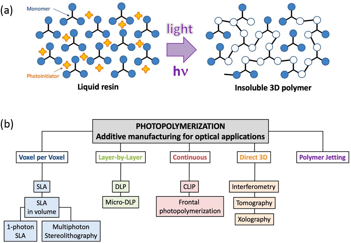
Figure 1.(a) Simplified schematic of the photopolymerization process involving the main components (photoinitiator and monomer). (b) The main photopolymerization-based additive manufacturing techniques described in this review.
2. PHOTOPOLYMERS FOR AM IN OPTICAL APPLICATIONS
A. Generalities
Regardless of its application, photopolymers generally comprise two principal compounds: 1) the photoinitiator(s) and 2) the monomer(s) and/or oligomer(s). The photoinitiator is a chemical compound (or an association of several molecules) that absorbs incident light and exploits excited electronic states to form reactive species capable of initiating the polymerization of monomers. The monomers are the elementary building units of the material, which link up to form a polymer.
The suitability of the photoinitiator (PI) depends on the wavelength of both the AM device used as well as the monomers. The absorption spectrum of the photoinitiator must at least partially cover the emission spectrum of the light source. Precisely stated, a good photoinitiator efficiently absorbs light of a desired wavelength and produces new chemical species that are extremely reactive toward the monomers from its excited states (PI*). Figure 2(a) provides the schematic of radical polymerization. Here, the radicals created from PI* induce the polymerization of monomer molecules through radical reactions. However, producing transparent materials using this method is susceptible to discoloration. Typically, wavelengths in the near UV range (below 405 nm) are preferred when manufacturing transparent materials, during which the photoinitiator is expected to be consumed. However, the reaction of the photoinitiator that generates photoproducts has different absorption properties. For example, in the case of acylphosphines, the oxide absorption spectrum shifts toward shorter wavelengths outside the visible spectrum, reducing the magnitude of absorption (photobleaching). Therefore, the consumption of the photoinitiator is difficult to achieve, and the leftover photoinitiator produces an undesired residual yellow coloration (for a photoinitiator absorbing in the near UV). In other cases, the photoproducts also cause coloration. This effect is relatively more sensitive as the object is thicker, the coloration being a cumulative effect in the thickness. Therefore, it is essential to optimize the concentration of the photoinitiator to ensure high reactivity and consequently faster manufacturing while avoiding residual coloration.
![]()
Figure 2.(a) Schematic representation of the radical photopolymerization process involving a photoinitiator (PI) absorbing a photon of energy
In addition, the monomer significantly influences the mechanical and optical properties of the final product and, hence, must be carefully selected. This is an advantage, considering that properties can be modulated by choosing the appropriate monomer or monomer mixtures to obtain properties intermediate between those of pure monomers. For example, refractive index can easily be modulated by selecting appropriate monomers [Fig. 2(b)]: 1H,1H,2H,2H-heptadecafluorodecyl methacrylate (HDFDMA) and 2,4,6-tribromophenyl acrylate have refractive indices of 1.38 and 1.60, respectively. Intermediate refractive indices can be obtained by mixing monomers of different indices. It should be noted that the fine control of the final index is a point that can be delicate to control because in photopolymer blends, it is necessary to manage the problems of miscibility (between monomers and between monomers and polymer), difference in reactivity, and diffusivity of the different monomers, which can especially impact the homogeneity of the material, and thus its optical and mechanical properties. These effects have been widely used for hologram storage and self-written waveguide applications, and the main results and concepts are described in the reviews [15,16]. However, these two monomers are monofunctional (carrying a single acrylate function). They do not permit the formation of cross-linked three-dimensional networks. Thus, they must be used in combination with difunctional monomers, such as TPGDA or an epoxy di(metha)crylate, which enables the modulation of the final mechanical properties of the material after polymerization. Depending on the application, other functionalities can also be obtained using monomers, oligomers, or fillers (including nanoparticles), such as wetting or dispersing agents, fillers, plasticizers, matting or gloss agents, pigments, and stabilizers.
Furthermore, photopolymerization can be classified into three types based on the type of chemical reaction involved: radical light curing and cationic or anionic polymerization. Among these, radical light curing is the most widely used. Cationic photopolymerization is typically used for certain coatings, and “hybrid” polymerization techniques also exist. Both are described below.
B. Radical Photopolymerization
In the case of radical photopolymerization, the reactive species are free radicals formed by the homolytic rupture of a bond in the excited state of the photoinitiator. The mechanisms are of two types: Norrish I and Norrish II [17] [Fig. 2(c)].
The Norrish I mechanism is based on the photocleavage of a single molecule into two radical fragments. This cleavage is easily achieved in the alpha position of a carbonyl group, which justifies the use of benzoin derivatives for this purpose (benzoin ether, halogenated ketones, dialkoxyacetophenones and diphenylacetophenones, morpholino and amino ketones, and hydroxy alkyl acetophenones among several other structures) [18]. Many commercial compounds, such as Darocur 1173 or Irgacure 184, are available [see Fig. 2(c)]. Their maximum absorption wavelengths are approximately 340/350 nm. In the case of acylphosphine oxides, such as Irgacure 819, the proximity of the phosphine group to the carbonyl group, induces a decrease in the energy of the electronic transition from the fundamental to the excited state, thereby permitting a shift in wavelengths toward the visible spectrum (400 nm). Type I photoinitiators are the most widely used in the industry since most photoinitiating systems operate using a single molecule.
The Norrish II mechanism involves the combination of a photoinitiator (PI) with a coinitiator or photosensitizer (PS). For such systems, the excitation wavelength corresponds to the absorption maximum of the photosensitizer, and it can be easily modulated by choosing the suitable photosensitizer in a large range of available compounds. This approach is particularly interesting for developing photoinitiator systems at the desired wavelength in the visible and near-infrared range. Ketone-/hydrogen-donor systems are popular examples of systems using the Norrish II mechanism [19]. These systems generally operate from their triplet state by electron transfer in the presence of an amine AH, which forms a charge transfer complex (CTC), followed by a proton transfer to form the radical species that initiate polymerization.
The monomers used in free radical polymerization are primarily acrylates and methacrylates. Moreover, a wide variety of monomers and oligomers are available, which enables the adjustment of chemical and physical properties of the photopolymerizable mixture and polymers over a wide range. This is particularly useful because the viscosities of common multifunctional monomers are too high to be used alone in 3D printing. In this case, a mixture of several monomers can be used to adjust the viscosity to ensure proper resin flow. These monomers are also susceptible to shrinkage, leading to distortions or deformations during layer-by-layer printing. For example, a maximum shrinkage of approximately 5% for bisphenol A dimethacryalte (bis-GMA) and 12% for triethylene glycol dimethacrylate (TEGMA) [20] have been reported. Another important feature of these formulations is their sensitivity to inhibition by oxygen [Fig. 2(d)] [21,22]. The oxygen dissolved in the resins can react with the excited species and radicals, leading to a loss in efficiency of the photopolymerization (speed and final conversion) and the appearance of a polymerization threshold. However, this phenomenon, which appears undesirable, can help stabilize formulation and can also be used to confine the polymerized zone spatially at the micrometric [23,24] or even nanometric scale [25–29]. Therefore, it is used in various 3D printing configurations.
It is noteworthy that materials based on acrylate monomers are generally brittle and glassy. To overcome this limitation, thiol-ene systems can be used, as their mechanical properties are easier to modify [30–32]. This leads to the formation of more homogeneous networks at the molecular level through the step-growth mechanism of polymerization [33,34]. Acrylate monomers reach the gel point at conversions of approximately 20%, while thiol-ene matrices reach this point at conversions of approximately 30% [1]. Consequently, materials obtained with acrylate monomers are more brittle and possess more stress. Thiol-ene materials are more ductile and simultaneously more resistant [35] due to the softer nature of the polymer.
A recent example of the complementary use of acrylate and thiol-ene systems in a 3D printing system called volumetric additive manufacturing [36] (detailed later) is shown in Fig. 3. The thiol-ene monomers used in this study are illustrated schematically in Fig. 3(a). Examples of 3D objects are presented in Fig. 3(b). Figure 3(c) compares the mechanical properties obtained with acrylate and thiol-ene based formulations, showing that the latter can be adapted over a wide range.
![]()
Figure 3.(a) Examples of acrylate (green) and thiol-ene (red-blue) monomers used in volumetric additive manufacturing, and the schematic structure of the prepared polymers. (b) An example of the 3D objects (scale bar 5 mm). (c) The illustration of the modularity of mechanical properties obtained using the thiol-ene systems [36].
In addition, these systems are less sensitive to oxygen, which eliminates the induction period and allows them to reach the dose to gelation more quickly for given irradiation conditions. Shrinkage is also minimized with these resins, which reduces the problems of deformation of formed objects.
C. Cationic Photopolymerization
In the case of cationic photopolymerization, diazonium, onium, iodonium, sulfonium, or pyrylium salts [37] are used to generate charged species to initiate the polymerization of specific monomers, usually from the epoxy resin family (Fig. 4).
![]()
Figure 4.(a) Schematic representation of the cationic photopolymerization process. (b) The photolysis mechanism of an iodonium salt. (c) The examples of epoxy monomers used in cationic photopolymerization.
Standard cationic photoinitiators have absorbances mainly in the UV spectrum below 300 nm. However, radical photoinitiators enable a shift in the absorption wavelength of the photoinitiator system up to 400 nm by photosensitization with anthracene or thioxanthone dyes, thus facilitating the use of low-cost LED as irradiation sources [38]. Furthermore, epoxy resins are the most widely used resins in 3D printing for their shrinkage rate of approximately 2%–3%, which is significantly less compared to that of conventional radical resins [1]. Moreover, once cured, they have good mechanical properties.
In contrast to conventional acrylate resins, cationic photopolymerization is not sensitive to oxygen. However, it is alcohol sensitive and is affected by conditions such as humidity. Furthermore, cationic photopolymerization is considered a “living polymerization” leading to a so-called “dark reaction” where the polymerization continues even after the irradiation is stopped and until the monomer is almost completely converted. This enables highly efficient conversion rates [39].
D. Hybrid Cure Photopolymerization and Dual Cure Systems
Hybrid systems can be used to combine the advantages of different polymerizations by including cationic and radical resins in the same mixture [40,41]. The objective is to create interpenetrating or semi-interpenetrating [42] networks using the two different modes of chain growth polymerization. The two types of networks develop independently of each other, either simultaneously (simultaneous propagations) or sequentially (successive propagations). This enables the combination of the advantages while simultaneously avoiding certain disadvantages, thereby obtaining different physicochemical resin properties. Highly reactive resins such as acrylates or vinyl ethers tend to create objects with stresses and deformations due to the high shrinkage rate. Combining them with methacrylate or epoxy resins reduces the rate of polymerization and shrinkage, thereby mitigating the risk of defects at the end of the printing process. Such approaches have been adapted to the constraints of additive manufacturing in different studies demonstrating the effectiveness of the approach through improved final properties [43]. One example in the context of optics is the use of hybrid resins to produce optical objects using conventional techniques such as laser stereolithography (SLA) or digital light processor stereolithography (DLP-SLA) by Wang et al. [44].
The term dual cure system is used when the polymer preparation is based on two-step polymerization processes. Several strategies are possible [45,46], two of which are particularly interesting for 3D printing.
The example structures in Fig. 5 illustrate the type of defects of refractive index homogeneity encountered in the polymer thickness. A trace of the layer-by-layer fabrication is clearly visible. In each polymerized layer, a gradient appears because the polymerization conditions are very different between the bottom and top of each layer. This difference is the consequence of the strong absorption in each polymerized layer, which is necessary to control the polymerized thickness at each step. These defects are thus reproduced in a periodic way. We can clearly see that this difference cannot be erased by UV post curing [Fig. 5(a)]. It can be seen in this same figure that thermal post-curing results in a more homogeneous material structure than UV post-curing. Moreover, in-depth treatment is easier to achieve by thermal treatment because the penetration depth of UV is limited [47].
![]()
Figure 5.Schematic view of the benefit of using a thermal post-cure versus UV post-cure. Thermal post-curing results in better homogeneity in the core of the polymer object. (a)–(f) are SEM images with different magnification of an object prepared by SLA with (a), (c), (e) UV post-cure and (b), (d), (f) thermal post-cure. The difference in structure is clearly visible by comparing (e) and (f). Bulk and surface homogeneity are critical parameters for optical applications [47].
The second step can also be an air or moisture treatment to induce the requisite complementary reaction.
E. Organic/Inorganic Hybrid Resins and Nanocomposites
The modification of properties can also be achieved by the synthesis of hybrid materials. Different photo-assisted preparation routes are possible. In the context of 3D printing by photopolymerization, these materials can be classified into two main categories according to the nature and interaction of the inorganic part: 1) hybrid materials prepared on the basis of organic/inorganic hybrid precursors and 2) hybrid materials prepared by incorporating inorganic (nano)fillers [48]. The final properties are modified by the presence of the inorganic phase, generally introduced at the molecular or nanometric scale, which enables the retention of transparency in the material by limiting the diffusion of light during manufacture and application. Optical, photonic, dielectric, and piezoelectric properties can be obtained along with mechanical properties improved by the presence of nanofillers [49].
In the first approach, materials based on organic/inorganic hybrid precursors are prepared in two steps [Fig. 6(a)]. In the first step, classical sol–gel reactions are induced to form an inorganic siloxane or metal-oxide network [52,53]. These precursors also contain a photopolymerizable part (acrylate or epoxy) that can be photopolymerized in the second step under conditions similar to those for the corresponding organic resins [54–56]. This enables the incorporation of
![]()
Figure 6.(a) Hybrid material approach based on organic/inorganic hybrid precursors in the context of 3D manufacturing by photopolymerization. The three precursors used react in solution by hydrolysis-condensation reactions (sol-gel chemistry) to form an inorganic network, which is cross-linked by UV irradiation. Examples of transparent parts are given (scale bar, 1 cm) [50]. (b) Nanocomposite approach by introducing silica nanoparticles in a light-curing matrix to fabricate 3D nanocomposite objects and subsequently sintering to mineralize the material. The examples of transparent silica parts that were made by this process are given (scale bar, 5 mm) [51].
An example of use for DLP structuring was proposed by Shukrun
The second approach to manufacturing hybrid materials employs fillers in the acrylate or epoxy resin. To maintain transparency and avoid light scattering phenomena, the fillers used are typically oxide nanoparticles (
The aforementioned examples illustrate the considerable diversity of photopolymerizable materials available for 3D printing applications. Different composition factors such as the nature and content of the photoinitiator, the addition of absorbers, and the choice of monomer enable the control of geometrical factors during fabrication (resolution in
3. POINT-BY-POINT MANUFACTURING TECHNOLOGIES
A. Laser Stereolithography (SLA)
Laser stereolithography (SLA) is the first described 3D printing technique that used photopolymerization. It was patented by André in 1984 [67] and, subsequently, by Hull in 1986 [68]. SLA is based on the use of a laser for the point-wise polymerization of a layer of liquid formulation [69]. The focused laser beam is deflected by galvanometric mirrors, which allows high writing speeds in the plane. Once the first layer has been produced, a platform moves a predetermined distance, corresponding to the thickness of a layer to be produced. The object is built voxel by voxel in the plane, independently of each other, and then layer by layer. Thus, it is possible to obtain complex and precise objects [Fig. 7(a)].
![]()
Figure 7.(a) Principle of the SLA [70]. (b) An example of the lenses manufactured by SLA, after production, and surface treatments by dipping in resins and polymerization (left, finished product) [71]. (c) The typical example of a surface defect [72]. (d) The examples of objects made with micro-SLA [73].
The ability to focus the laser spot enables a high spatial resolution in
The total manufacturing time required for a part depends on two related criteria. The first is the
The main advantage of the SLA technique is the high precision possible through the use of a laser focused on each point of the material. This enables the production of a large variety of objects using precise control of the initial CAD modeling. This flexibility is obviously of great significance for the manufacture of optical objects since it is possible to generate flat or curved surfaces as required.
Presently, companies that commercialize SLA machines offer resins that enable the production of translucent or transparent objects. However, in general, the manufactured objects do not meet the quality criteria required for optical applications, both with regard to the bulk properties of the material and the surface properties. The technologies developed to improve the bulk properties (especially continuous and direct 3D writing) are discussed in Sections 4 and 5. With respect to surface properties, the objects at the output of the 3D printing machine generally possess surface irregularities. These can be eliminated by the post-treatments that are commonly used in optics, such as a polishing step, or the addition of a coating that will also help obtain optical surface with nanometric roughness [Fig. 7(b)] [71].
Considerable work has been done recently to improve the quality of 3D-printed optical objects to ensure they meet the requisite specifications. For example, it has been established that surface irregularities can be reduced by decreasing the size of the voxels printed in the resin. However, Gaussian surface defects [Fig. 7(c)] [72] caused by the diffusion of light through the illuminated resin are a significant challenge. To overcome this, micro-SLA techniques have been developed. Stampfl
Another feature that was developed in these processes is the capability of thickness manipulation. To reduce the thickness of the layers produced, two possibilities are considered [75]. The first is to irradiate the resin with small doses of light, close to the threshold dose of the formulation. However, this step has a major drawback. Unless the point-wise dosage is precisely controlled, unwanted irradiation of nearby points might cause undesirable results since the threshold of each point can vary marginally. An example of this is pieces requiring high and low densities of pixels in the fabrication plan. The second technique involves adjusting the absorbance of the resin, for which additives such as UV absorbers are used to reduce the penetration depth at the desired wavelength.
The reduction of layer thickness must also be carefully implemented from a certain thickness, especially when using a scraper to generate extremely thin layers. [76] This limit is approximately ten microns [73]. Below that, mechanical refilling of the formulation can easily damage small details on the previously cured layer. In addition, the range of compatible resin viscosities is even narrower than in a conventional SLA technique. The flatness of the free surface to be irradiated is also difficult to control. However, the detachment of the polymerized layer from this window becomes difficult at low polymer thicknesses.
This limitation can be overcome by switching from layer-wise laser writing to direct writing in the volume. This strategy avoids the time-intensive refill step, which generates defects, and limits the applicable viscosity range of the resins. In general, considering that the generation of defects is directly related to the selected process, direct writing can prevent most problematic defects in the targeted application [77]. Direct writing in the volume approaches is described in the following section.
B. SLA in the Volume in Single-photon Absorption Regime
Another approach to overcoming the problems associated with the photopolymer layer refill step is to directly focus a laser into the photopolymer volume to fabricate the object by inducing point-wise (voxel-wise) polymerization reactions at the focal point of the laser across the surface of the object.
The irradiated area can be displaced in two ways: with a mobile writing beam using galvanometric mirrors or with a mobile resin tank on piezoelectric plates. The first solution enables faster writing speeds. Regardless, in both cases, the resin remains immobile during the manufacturing process without any constraint on its ability to flow, which enables the use of extremely viscous resins.
Fundamentally, the primary challenge is to ensure that the cross-linking of the photopolymer is induced solely at the focal point of the laser and not on the rest of the writing beam path. However, this is highly probable based on two principles. The power density is maximum at the focal point, and above all, the resin presents a non-linear response, characterized by the existence of a polymerization threshold. For energies below this threshold, the resin is not sufficiently cross-linked and remains soluble under the usual development conditions. Above the polymerization threshold, the resin resists development. As mentioned previously, this behavior is largely controlled by the intervention of inhibitors in the resin (oxygen for acrylate resins following a radical mechanism and acids/bases). It is noteworthy that these inhibitors can be released by light (at the same or different wavelength), which imparts an extra degree of flexibility to them. This concept is used for the simulation emission depletion (STED) and xolography technologies, which are discussed later in this review.
Moreover, the achievable resolution is dependent on the resolution of the optical system used to focus the laser light, usually a large numerical aperture microscope objective. The resolution is directly related to the irradiation wavelength and the device used. But it also depends strongly on the response of the photopolymer.
In practice, obtaining high resolutions poses several problems. The working distance of the microscope objective can become extremely small. Thus, solutions were proposed in which the objective is immersed directly in the resin. Problems can also be related to inhomogeneities in the resin that disturb the propagation of the writing beam. This becomes critical when the size of the objects to be manufactured increases.
For single-photon absorption photopolymerization, convincing demonstrations have been presented by writing at 532 nm in UV resins [78,79], specifically, in a commercial cationic UV resin (SU8) with laser writing based on the ultra-low photon absorption (LOPA) technique. The resin and the laser conditions are selected to ensure that the polymerization is only effective at the focal point. Complex 3D structures, such as chiral spirals and woodpiles, with sizes as small as 190 nm, have been fabricated using a continuous laser at 532 nm (a few mW) and a commercial photoresist (SU8) (Fig. 8). Compared to the TPA technique described in the following section, this technique exhibits several advantages, such as simplicity and low cost.
![]()
Figure 8.(a) Experimental setup for low one-photon absorption (LOPA) photolithography. (b) Absorption spectrum of the resin (SU8) showing the very low absorbance of the resin at the wavelength used (532 nm). (c) and (d) Examples of structures prepared by LOPA [78,79].
C. Multiphoton Stereolithography
Another method that has developed considerably in recent years to obtain 3D microstructures by direct laser writing is biphoton, or more generally, multiphoton SLA [80,81]. This method uses two-photon absorption (TPA), which is the simultaneous absorption of two photons of the same or different energies to excite a molecule in a given state (usually the ground state) to a higher energy electronic state. The energy difference between these two states is equal to the sum of the energies of the two photons. The same effect can be obtained by the absorption of three or more photons corresponding to multiphoton absorption. This effect was first predicted theoretically by Maria Goeppert-Mayer [82] and then demonstrated experimentally using pulsed laser sources. Two-photon absorption is a second-order process, several degrees of magnitude smaller than linear absorption. It differs from linear absorption because it is proportional to the square of the intensity of the light, making it a nonlinear optical process. This nonlinearity enables the confinement of the photo-induced reaction in a volume smaller than the irradiated volume, resulting in a higher resolution. This concept was widely used for high-resolution fluorescence microscopy and later for SLA. Moreover, two-photon photopolymerization can be induced solely at the focal point without affecting the material along the beam path before or after the focal point. In addition, TPA requires the use of a laser with a very short pulse duration (a few tens or hundreds of femtoseconds), strongly focused inside the volume of a photopolymer. Under such conditions, the high density (spatial and temporal) of photons can induce a multiphoton absorption in the focal volume [83]. In the presence of a suitable photoinitiator showing good TPA properties, the local curing of the resin is thus obtained locally. This technique enables the conditions conducive to direct writing in the resin with excellent resolutions.
Since Kawata’s proof of principle in 1997 [84,85], great progress has been made in the development of resins and instrumentation. For one, more and more efficient photoinitiators are available, enabling a significant increase in the writing speed [86]. Regarding the instrumentation, several devices are now commercialized (Nanoscribe, Multiphoton Optics, Microlight, etc.). Moreover, in most cases, the wavelength used is in the infrared range (around 800 nm).
The primary advantage of this technique for the manufacturing of optical objects is the extreme precision that enables the manufacturing of optical micro-elements with excellent surface finish. The examples shown in Fig. 9 [87,88] present microlenses manufactured at the end of the optical fiber and various basic optical elements (mirrors, lenses, and beam-expanders), respectively. In both cases, the sharpness of the writing beam enables surface conditions compatible with optical applications. The other advantage of the technique is that these objects can be integrated onto various supports, such as optical fiber outlets.
![]()
Figure 9.Examples of optical microelements fabricated by biphotonic stereolithography [87,88].
Furthermore, various strategies have been developed to obtain resolutions below the diffraction limit. For example, Takada
These ultra-resolution techniques are, however, limited by the lengthy fabrication time, which is impractical in the industrial production of optical objects. To facilitate the application of these techniques to large objects, various approaches were developed, including parallel writing using multiple beams. Nielson
Finally, when comparing the performance of voxel-by-voxel AM techniques, it is important to consider not only the minimum voxel size (resolution) but also the maximum voxel printing speed to adequately cover the manufacturing needs of complex objects, combining relatively large size and high-resolution details. The ability to manage the precision of stitching between voxels or parts is also an important challenge in the fabrication of optical parts with important dimensions. In this context, several approaches based on two-photon absorption have been proposed such as multi-focus two-photon printing [96] or two-photon printing with an ultrafast random-access digital micromirror device (DMD) scanner [97]. Binary holography was also proposed to realize aberration-free large-area stitch-free 3D printing [98]. These techniques allow the fabrication of large-area complex 3D structures such as metamaterial structures, micro-lenses, and 2D gray level diffractive optical elements (DOEs) with better than 100 nm resolution and they have competitive DMD pattern rates, which reinforces the interest of approaches based on biphotonic absorption.
Approaches of parallelization of the manufacturing by spatial and temporal focusing of a femtosecond laser have also been proposed. This allows a layer-by-layer parallelization fabrication of arbitrary 3D structures based on a projection principle. The writing speed can be increased by 3 orders of magnitude, which also opens perspectives for large scale manufacturing while maintaining the resolution of two-photon printing [99,100].
Another advantage lies in the possibility of preparing different types of materials, thus modulating the refractive index for a given application [66] with sol–gel chemistry, or the incorporation of passive or active optical functions with metallic nanoparticles [101] or liquid crystals [102].
4. LAYER-BY-LAYER DLP
Digital light processing (DLP) is an SLA technique using a light projection system [103–106]. In most cases, an LED lamp is used. In some specific configurations, a mercury lamp was implemented [107]. Moreover, the light source is used in combination with a matrix of dynamic mirrors (DMD), enabling the spatial structuring of the light [108,109] in the form of a pixelated image. The dimension of the projection of the pixels at the focal point determines the resolution
The layer-wise manufacturing can be done starting from the bottom or top layer of the object. The first case, also called “bottom-up,” is mostly used because it enables the process speed to be optimized by decreasing the time required for the refill of material [110]. The formulation tank used is smaller than the final object and the material refill is done with a pump, thereby reducing waste. This configuration also reduces the physical and chemical impact of the resin on the process. There is no need to use a scraper to level the surface and interaction with oxygen is greatly reduced. This allows the use of a wider range of viscosities.
DLP facilitates higher resolutions with minimal impact on writing time. In the case of SLA, the manufacturing time is proportional to the
As with SLA writing, layer-by-layer fabrication can generate “stepped surface” defects on curved surfaces that make the fabricated objects unusable for optical applications. These aspects were studied on pixel arrays, lines, and also at the single pixel scale in Ref. [111]. The results revealed that the nature of the monomers used in the resin significantly affected the surface homogeneity of the manufactured objects. Chen
![]()
Figure 10.(a) DLP technology with grayscale writing. (b) An example of a lens made by DLP using the post-polymerized meniscus strategy and grayscale writing. (c) The comparison between the classical DLP approach (top) and post-polymerization and grayscale approach [112].
Several “continuous” techniques have been developed as follow-ups to DLP technology which provide improved object quality and reduced manufacturing time. They are the subject of the following section.
5. CONTINUOUS MANUFACTURING PROCESSES
A. CLIP Technology
The continuous liquid interface production (CLIP) technique is a continuous technique derived from DLP. Fundamentally, instead of layer-wise production, this process generates the object about the transverse axis in a continuous manner. From a physico-chemical point of view, the technique is based on the generation and control of a light-curing reaction inhibition zone, or a “dead zone,” to maintain a non-polymerized formulation layer throughout the process. This liquid layer is located as close as possible to the irradiation zone and enables constant movement of the platform and replenishment of the resin. The images projected by the lamp will scroll continuously in accordance with the movement of the platform.
This phenomenon of inhibition can be ensured in two ways: either by the action of molecular oxygen or by a photoinhibitor, i.e., a species inhibiting the polymerization reaction generated by light irradiation. The first approach was developed by De Simone
![]()
Figure 11.(a) Schematic diagram of the CLIP technology [114]. (b) Schematic diagram of the CLIP technology with the photoinhibitor [116]. (c) The illustration of the influence of the choice of slicing on the roughness of objects manufactured by CLIP [115]. (d) The examples of lenses manufactured by micro-CLIP. The roughness suppression on the right example is obtained by depositing a resin layer in post-processing [117].
The photoinhibitor approach is based on a device that irradiates the resin with two distinct wavelengths, each of which has a specific role [116]. One wavelength is used to generate the images corresponding to the shape to be manufactured by photopolymerization (in this example 365 nm). The second wavelength (470 nm in this example) is used to generate polymerization inhibitors by a photochemical process [Fig. 11(b)]. These are responsible for blocking the polymerization and the layer in liquid form. Photoinitiators such as HABI (Norrish type 2) are used. Without a co-initiator, they play a role of carbo-centric radical inhibitors. An interesting aspect of this approach is that the relative kinetics of polymerization and inhibition can be easily modulated by changing the relative intensity of the irradiations at both wavelengths. This parameter enables easy management of the thickness of the uncured layer, in contrast to the oxygen inhibition approach.
The continuous manufacturing mode has two primary advantages. The material refill, the most time-consuming step in conventional SLA, is performed continuously, which significantly accelerates the process. However, this assumes that the resin has a low viscosity suitable for efficiently flowing into the inhibition volume. This becomes even more crucial in manufacturing objects with larger cross-sections. The second interesting point is an improved homogeneity of the material resulting from the elimination of discontinuities owing to the sequential nature of the process. The obtained objects are isotropic, thus presenting identical mechanical and optical properties in all spatial directions. Figure 11(c) shows the effect of slicing on the roughness of the objects and the possibility of generating a smooth object using CLIP technology.
CLIP technology is commercialized by carbon with applications in the fields of dentistry, automotive engineering, and shoe soles. In the field of optics, there are examples based on micro-CLIP technology [Fig. 11(d)] [117]. This technique enables significant reduction of manufacturing time, in contrast to classical DLP technology. The nature of the membrane and its ability to let oxygen through are important parameters for obtaining the desired quality. The surface roughness is particularly dependent on the membrane. However, these defects can be eliminated by the meniscus technique, which involves depositing a layer of resin of the same nature after the manufacturing process and post-polymerizing using UV.
CLIP technology has been extremely popular in the last few years and has become one of the leading volume average theory (VAT) techniques. However, despite the clear advantages in terms of fabrication speed and isotropy of the final material properties, its use for the fabrication of massive and solid parts for optics (such as ophthalmic lenses) is limited because it supposes that the resin can flow quickly to fill the consumed resin. This viscosity criterion of the usable resins considerably limits the range of usable resins.
B. Frontal Photopolymerization
Frontal photopolymerization (FPP) is another continuous 3D printing technique. It is based on the continuous propagation of a polymerization front through a formulation perpendicular to the irradiated substrate [Fig. 12(a)]. Here, in contrast to CLIP, the polymerization starts on the first interface and then propagates in the opposite direction in the tank without moving a stage. A patent from ophthalmic industry has recently presented the use of FPP combining light energy modulation in the plane and the use of a photo-bleaching photoinitiator to generate curved surfaces [121]. The heights cured are controlled directly from the light dosage provided by the light source. The propagation of the polymerization front is therefore controlled by the absorption of the resin in the depth. In general, the absorbance of the photoinitiators decreases during the polymerization (photobleaching), which enables polymerized thicknesses of a few mm [118]. However, if the resin has a constant or even increasing absorption during curing, then the maximum thickness is limited [122].
![]()
Figure 12.(a) Schematic diagram of the FPP approach [118]. (b) The example of 3D objects manufactured by FPP based on different monomer chemistries [119]. (c) The examples of micro-lenses manufactured by FPP at the end of an optical fiber [120].
The advantage of this approach is the absence of the layering step, thus considerably reducing the fabrication time. It should be noted, however, that the principle of propagation polymerization can lead to property gradients depending on the direction of manufacturing. The consequences can be negative (stress generation), but the approach has been shown to be easily programmable to control the deformation of non-optical objects, using origami-like techniques [123].
Figures 12(b) and 12(c) show basic objects fabricated with different types of photopolymers. More specifically, Fig. 12(c) shows the same principle applied to the micrometric scale, which enables manufacturing of micro-lenses by FPP at the outlet of an optical fiber. The principle is based on the use of the beam transmitted in the core of the fiber to manufacture the lens by F3P. It can also be applied to UV wavelengths [124], visible wavelengths [125], or in the infrared spectrum [24,120]. These SEM images reveal the excellent surface quality that can be obtained in this configuration on optical fiber. These results can be compared with those shown in Fig. 9 which enable the generation of more complex structures but also involve a much more complex technology. Although this technique is limited to the fabrication of solid objects (also called 2.5D fabrication), it has significant potential for microfluidic applications [126], electronics [127] for polymers such as acrylate, epoxy, and also nanocomposites filled with CNT or silica particles [128]. Continuous approaches can, therefore, limit the defects inherent in point-wise and layer-wise manufacturing. Therefore, new approaches have been proposed to fabricate the 3D object in a single step, within the resin.
C. Light-assisted Polymer Jetting
Besides the aforementioned AM techniques, the technique of polymer jetting assisted by UV or NIR irradiation is also a relevant alternative technique for the fabrication of large optical objects with excellent surface quality.
Material jetting 3D printing was patented by Objet Ltd. in 1999. The concept involves combining inkjet technology, used by conventional 2D printers on paper, and photopolymers. The print head projects micro-droplets of photopolymer resin onto the substrate [Fig. 13(a)] [129]. A light source (LED or laser) is integrated into the print head and hardens the material to form the first layer. The following layers can then be manufactured in successive layers. The irradiation used is usually UV, which enables the use of the photopolymers described in Section 1 of this review. An example of irradiation in the infrared spectrum to fabricate lenses in polydimethylsiloxane (PDMS) is presented in Ref. [130].
![]()
Figure 13.(a) Schematic of the polymer jetting technique [129]. (b) The example of a lens (center) made from the model (left) and the characterization of the surface (right) [129]. (c) The characterization of the surface roughness of the objects [131].
The technique enables excellent resolutions, owing to the small size of the droplets that can be generated. The resolution is related to the viscosity of the formulation, its affinity for the substrate, the cross-linked polymer, and the ejection speed of the nozzles.
This technology especially enables the generation of extremely smooth surfaces by exploiting the fact that the final surface corresponds to drops spread, which are subsequently polymerized. Thus, it enables the production of optical surfaces without post-treatment [Fig. 13(b)]. Assefa
Although it is not significant for optical applications, another advantage of the technique is the possibility of fabricating multi-material objects. The fabrication time is relatively small due to the elimination of the resin refill step of conventional processes and the optimization of the reactivity of the UV photopolymers used.
Droplets of resin formulation that are 17 μm in diameter are deposited on a flat substrate using three print heads, each with 1000 nozzles. The layers have a thickness of 4.1 μm. The substrate is a glass slide, silanized to improve adhesion. Four seconds are required to create and polymerize a
7. EMERGING NEW TECHNOLOGIES: INSTANT 3D MANUFACTURING
We have seen in the aforementioned processes that an important limitation is linked to layer-wise or voxel-wise fabrication strategies. Not only does this approach significantly increase the fabrication time but also results in anisotropic fabrication. Therefore, it is difficult to ensure homogeneous properties throughout the volume of the object. Consequently, this results in optical defects that adversely affect several optical applications.
Therefore, new approaches to 3D manufacturing were developed. They can be described as instant manufacturing or the manufacturing of the object being performed for the entire volume of the object to be manufactured in a single step.
As for the SLA manufacturing in the volume (LOPA and TPS), the primary challenge is to manage the propagation of the beam in the resin until it reaches the zone where it must be “active.” Here, the light is generated outside the photopolymer and must therefore propagate to the zone where it must activate the polymerization reaction without significantly modifying the resin on its optical path.
A. Single Step Volumetric AM of Complex Polymer Structures
Until recently, 3D volumetric structures realized in a single step were demonstrated solely in interference lithography [133,134]. More or less complex approaches combining up to five coherent beams enable the creation of periodic structures that are sub-micrometer lattices, presenting very interesting properties in optics, photonics, or sensors. Multiple beams can also be generated by phase masks [135]. However, these approaches are limited to relatively thin films and to produce periodic structures. In this case, polymerization occurs in constructive interference volumes. In destructive interference volumes, the photonic conditions are selected to remain below the polymerization threshold, and thus the 3D piece is obtained after elimination of the non-reacting resin.
These interferometric approaches involve phase-controlled coherent beams, which result in the interference in the resin. Shushteff
![]()
Figure 14.(a) Scheme of the experimental set-up for the volumetric AM in one step and examples of realizations. (b) The comparison of the performance of this technique with the main AM techniques [136].
B. Computed Axial Lithography
In the previous example, the object must be generated from three beams that irradiate the resin simultaneously. A recently proposed alternative is based on the same principle of depositing locally in 3D the dose necessary for polymerization. However, in this case, the accumulation of light progresses through successive irradiations by changing the angle of incidence between irradiations [137].
The computed axial lithography method (CAL) [138] is thus designed to expose the transparent resin by projecting 2D images at different angles around an azimuthal axis. The approach is largely inspired by a cancer treatment technology used in radiology, intensity modulated radiation therapy (IMRT) [139]. A major component of this technology was the development of a computational algorithm to design the projected image from each angle based on a target.
Figure 15 illustrates the potential of the technique. The reproduction of Le Penseur from Auguste Rodin has been realized by projecting multiple images in the resin [Fig. 15(a)]. The images are generated by a classical DLP projector, which diffuses the series of images by synchronization with the rotation angle of the resin tank [Fig. 15(b)]. The sequence of photographs [Fig. 15(c)] shows the sequence of images in the manufacturing time of less than a minute. Examples of the fabrication are given in Fig. 15(d).
![]()
Figure 15.(a) Schematic of the axial volume lithography technique, (b) schematic of the device, (c) photographs of the sample being fabricated, and (d) examples of objects fabricated with this technique in different materials and sizes [137].
From a chemical point of view, this principle is based on the possibility of very precisely controlling the photopolymerization threshold. It should be noted that the threshold observed is the gelation threshold, which corresponds to the threshold beyond which the material is sufficiently resistant to withstand post-processing (development in a solvent) while remaining attached to neighboring material (adjacent layer or voxel). This threshold is, from a definition point of view, different from the polymerization initiation threshold defined as the threshold at which the conversion of monomers into polymer starts. This threshold is itself closely related to the inhibition threshold, which corresponds to the dose necessary to consume the inhibitors in the formulation (including oxygen, generally in radical photopolymerization). The conversion of monomers starts efficiently only when the inhibitor concentration has dropped below a threshold concentration. The light profiles projected in the resin ensure that for each point in space, a dose of energy is deposited. If this dose is below the threshold, then the resin is not insufficiently exposed and will be eliminated during development. If the threshold dose is exceeded, then the cross-linking of the polymer network is sufficient to resist the solvent and the part is formed.
Such a technology appears extremely interesting for the rapid generation of macroscopic objects more homogeneous than by layer-wise or point-wise manufacturing. However, the complexity of the decomposition of the object into images for the different angles can limit the practical applications, primarily because this decomposition depends on the resin used. In particular, the problems of absorption by the resin on the beam path must be integrated, which limits the size and resolution of the accessible objects. Typically, a resolution of the order of 300 μm is obtained. Recently, the resolution has been improved by an optimization of the process [140]. However, this technology seems very well adapted to produce rotationally symmetrical objects such as optical elements in general.
C. Xolography
A new volumetric approach, xolography, has recently been proposed [141]. This is a two-color technique based on the use of photocommutable photoinitiators. By irradiation at the wavelength
Thus, the inhibition wavelength
![]()
Figure 16.(a) Schematic of the xolography technique and specific photocommutable photoinitiator synthesized at the base of this approach. The spectrum of the photoinitiator in its initial form is in black, and after irradiation in the UV (
8. CONCLUSION
This review illustrates the advantages and the diversity of recently developed approaches using UV processes for optical applications in the field of additive manufacturing. In the field of optics, these technologies have the following advantages: rapid transition from design to component with infinite possibilities of customization, possibility of obtaining desired properties by incorporating different materials, capability of fabricating complex structures to obtain (multi)functional objects, and reduction of environmental damage by reducing wastage as compared to subtractive processes. Furthermore, the contribution of photopolymerization enables the use of green energy and limits the use of environmentally polluting solvents.
However, these technologies neither completely satisfy the requirements of optical applications nor exhibit performances comparable to those of conventional processes. In conclusion, these techniques require further improvement in several criteria, such as high fabrication speed combined with sub-micrometer scale fabrication precision, homogeneity and isotropy of the final material, refractive index control, and surface finish.
Nevertheless, in comparison to the initial AM technologies that were not dedicated to optical applications, considerable progress has been made. However, no single technology has become the absolute reference in the field of optics. Primarily, the manufacturing speed must be improved while guaranteeing homogeneous optical properties. Moreover, the finished product must possess an optical quality surface, enabling direct use, without any additional post-processing. In addition, active functions can be integrated into the finished products [142]. One possible method for this is the integration of functional materials such as photochromic, electrochromic, luminescent, and (semi)conductive molecules or particles.
Considering the recent results presented in this review, these advances will be possible only through interdisciplinary work involving fundamental advances in fields as diverse as photochemistry, physical chemistry, and macromolecular chemistry. Furthermore, the development of the irradiation devices is critical to achieving the required optimal technique. This requires technological developments of hardware, software, optics to master the manipulation of the irradiation beam, and its action on the photopolymer.
Acknowledgments
Acknowledgment. The authors thanks ANRT (France) for financial support (Convention CIFRE N° 2018/1027).
APPENDIX A: ABBREVIATIONS
References
[1] S. C. Ligon, R. Liska, J. Stampfl, M. Gurr, R. Mülhaupt. Polymers for 3D printing and customized additive manufacturing. Chem. Rev., 117, 10212-10290(2017).
[2] M. Kalender, S. E. Kılıç, S. Ersoy, Y. Bozkurt, S. Salman. Additive manufacturing and 3D printer technology in aerospace industry. 9th International Conference on Recent Advances in Space Technologies (RAST), 689-694(2019).
[3] R. Leal, F. M. Barreiros, L. Alves, F. Romeiro, J. C. Vasco, M. Santos, C. Marto. Additive manufacturing tooling for the automotive industry. Int. J. Adv. Manuf. Technol., 92, 1671-1676(2017).
[4] W. K. Durfee, P. A. Iaizzo. Medical applications of 3D printing. Engineering in Medicine, 527-543(2019).
[5] J. Sun, W. Zhou, J. Y. H. Fuh, G. S. Hong. An overview of 3D printing technologies for food fabrication. Food Bioprocess Technol., 8, 1605-1615(2015).
[6] G. Wang, X. Zhu, J. Wu, J. Zhu, X. Chen, Z. Cheng. Synthesis and photoinduced surface-relief grating of well-defined azo-containing polymethacrylates via atom transfer radical polymerization. J. Appl. Polym. Sci., 106, 1234-1242(2007).
[7] Y. Zhang, W. Zhang, X. Chen, Z. Cheng, J. Wu, J. Zhu, X. Zhu. Synthesis of novel three-arm star azo side-chain liquid crystalline polymer via ATRP and photoinduced surface relief gratings. J. Polym. Sci. A, 46, 777-789(2008).
[8] S. Jradi, O. Soppera, D. J. Lougnot. Fabrication of polymer waveguides between two optical fibers using spatially controlled light-induced polymerization. Appl. Opt., 47, 3987-3993(2008).
[9] M. Sangermano, B. Voit, F. Sordo, K.-J. Eichhorn, G. Rizza. High refractive index transparent coatings obtained via UV/thermal dual-cure process. Polymer, 49, 2018-2022(2008).
[10] A. Nebioglu, J. A. Leon, I. V. Khudyakov. New UV-curable high refractive index oligomers. Ind. Eng. Chem. Res., 47, 2155-2159(2008).
[11] S. Murase, K. Kinoshita, K. Horie, S. Morino. Photo-optical control with large refractive index changes by photodimerization of poly(vinyl cinnamate) film. Macromolecules, 30, 8088-8090(1997).
[12] L. V. Natarajan, D. P. Brown, J. M. Wofford, V. P. Tondiglia, R. L. Sutherland, P. F. Lloyd, T. J. Bunning. Holographic polymer dispersed liquid crystal reflection gratings formed by visible light initiated thiol-ene photopolymerization. Polymer, 47, 4411-4420(2006).
[13] S. H. Cho, F. S. Tsai, W. Qiao, N.-H. Kim, Y.-H. Lo. Fabrication of aspherical polymer lenses using a tunable liquid-filled mold. Opt. Lett., 34, 605-607(2009).
[14] C. Zimmerman, M. White, M.-E. Baylor. Effects of varying interfacial surface tension on macroscopic polymer lenses. Opt. Eng., 54, 097108(2015).
[15] R. Malallah, H. Li, D. P. Kelly, J. J. Healy, J. T. Sheridan. A review of hologram storage and self-written waveguides formation in photopolymer media. Polymers, 9, 337(2017).
[16] B. Kowalski, R. R. Mcleod. Design concepts for diffusive holographic photopolymers. J. Polym. Sci. B, 54, 1021-1035(2016).
[17] B. Steyrer, P. Neubauer, R. Liska, J. Stampfl. Visible light photoinitiator for 3D-printing of tough methacrylate resins. Materials, 10, 1445(2017).
[18] J.-P. Fouassier, J. Lalevée. Photoinitiators for Polymer Synthesis: Scope, Reactivity and Efficiency(2012).
[19] J. Fouassier. Photoinitiation, Photopolymerization, and Photocuring: Fundamentals and Applications(1996).
[20] L. U. Kim, J. W. Kim, C. K. Kim. Effects of molecular structure of the resins on the volumetric shrinkage and the mechanical strength of dental restorative composites. Biomacromolecules, 7, 2680-2687(2006).
[21] M. Höfer, N. Moszner, R. Liska. Oxygen scavengers and sensitizers for reduced oxygen inhibition in radical photopolymerization. J. Polym. Sci. A, 46, 6916-6927(2008).
[22] R. Li, F. J. Schork. Modeling of the inhibition mechanism of acrylic acid polymerization. Ind. Eng. Chem. Res., 45, 3001-3008(2006).
[23] C. Croutxé-Barghorn, O. Soppera, L. Simonin, D. Lougnot. On the unexpected role of oxygen in the generation of microlens arrays with self-developing photopolymers. Adv. Mater. Opt. Electron., 10, 25-38(2000).
[24] I. Dika, F. Diot, V. Bardinal, J.-P. Malval, C. Ecoffet, A. Bruyant, D. Barat, B. Reig, J.-B. Doucet, T. Camps, O. Soppera. Near infrared photopolymer for micro-optics applications. J. Polym. Sci., 58, 1796-1809(2020).
[25] A. Khitous, C.-F. Lin, F. Kameche, H.-W. Zan, J.-P. Malval, D. Berling, O. Soppera. Plasmonic Au nanoparticle arrays for monitoring photopolymerization at the nanoscale. ACS Appl. Nano Mater., 4, 8770-8780(2021).
[26] C. Deeb, C. Ecoffet, R. Bachelot, J. Plain, A. Bouhelier, O. Soppera. Plasmon-based free-radical photopolymerization: effect of diffusion on nanolithography processes. J. Am. Chem. Soc., 133, 10535-10542(2011).
[27] C. Deeb, X. Zhou, D. Gérard, A. Bouhelier, P. K. Jain, J. Plain, O. Soppera, P. Royer, R. Bachelot. Off-resonant optical excitation of gold nanorods: nanoscale imprint of polarization surface charge distribution. J. Phys. Chem. Lett., 2, 7-11(2011).
[28] F. Kameche, W. Heni, S. Telitel, L. Vidal, S. Marguet, L. Douillard, C. Fiorini-Debuisschert, R. Bachelot, O. Soppera. Probing plasmon-induced chemical mechanisms by free-radical nanophotopolymerization. J. Phys. Chem. C, 125, 8719-8731(2021).
[29] F. Kameche, W. Heni, S. Telitel, D. Ge, L. Vidal, F. Dumur, D. Gigmes, J. Lalevée, S. Marguet, L. Douillard, C. Fiorini-Debuisschert, R. Bachelot, O. Soppera. Plasmon-triggered living photopolymerization for elaboration of hybrid polymer/metal nanoparticles. Mater. Today, 40, 38-47(2020).
[30] M. Sahin, S. Ayalur-Karunakaran, J. Manhart, M. Wolfahrt, W. Kern, S. Schlögl. Thiol-Ene versus binary thiol-acrylate chemistry: material properties and network characteristics of photopolymers. Adv. Eng. Mater., 19, 1600620(2017).
[31] H. B. Song, A. Baranek, B. Worrell, W. D. Cook, C. N. Bowman. Photopolymerized triazole-based glassy polymer networks with superior tensile toughness. Adv. Funct. Mater., 28, 1801095(2018).
[32] T. J. McKenzie, P. S. Heaton, K. Rishi, R. Kumar, T. Brunet, G. Beaucage, O. Mondain-Monval, N. Ayres. Storage moduli and porosity of soft PDMS PolyMIPEs can be controlled independently using thiol–ene click chemistry. Macromolecules, 53, 3719-3727(2020).
[33] C. E. Hoyle, T. Y. Lee, T. Roper. Thiol–enes: chemistry of the past with promise for the future. J. Polym. Sci. A, 42, 5301-5338(2004).
[34] C. E. Hoyle, C. N. Bowman. Thiol-ene click chemistry. Angew. Chem. Int. Ed., 49, 1540-1573(2010).
[35] H. Lu, J. A. Carioscia, J. W. Stansbury, C. N. Bowman. Investigations of step-growth thiol-ene polymerizations for novel dental restoratives. Dental Mater., 21, 1129-1136(2005).
[36] C. C. Cook, E. J. Fong, J. J. Schwartz, D. H. Porcincula, A. C. Kaczmarek, J. S. Oakdale, B. D. Moran, K. M. Champley, C. M. Rackson, A. Muralidharan, R. R. Mcleod, M. Shusteff. Highly tunable thiol-ene photoresins for volumetric additive manufacturing. Adv. Mater., 32, 2003376(2020).
[37] M. Lecompère, X. Allonas, D. Maréchal, A. Criqui. Versatility of pyrylium salt/vinyl ether initiating system for epoxide dual-cure polymerization: kick-starting effect of the coinitiator. Macromol. Rapid Commun., 38, 1600660(2017).
[38] M. Sangermano, N. Razza, J. V. Crivello. Cationic UV-curing: technology and applications. Macromol. Mater. Eng., 299, 775-793(2014).
[39] F. Petko, M. Galek, E. Hola, R. Popielarz, J. Ortyl. One-component cationic photoinitiators from tunable benzylidene scaffolds for 3D printing applications. Macromolecules, 54, 7070-7087(2021).
[40] J.-D. Cho, J.-W. Hong. UV-initiated free radical and cationic photopolymerizations of acrylate/epoxide and acrylate/vinyl ether hybrid systems with and without photosensitizer. J. Appl. Polym. Sci., 93, 1473-1483(2004).
[41] J. V. Crivello. Hybrid free radical/cationic frontal photopolymerizations. J. Polym. Sci. A, 45, 4331-4340(2007).
[42] L. Chikh, V. Delhorbe, O. Fichet. (Semi-)Interpenetrating polymer networks as fuel cell membranes. J. Membr. Sci., 368, 1-17(2011).
[43] J. W. Kopatz, J. Unangst, A. W. Cook, L. N. Appelhans. Compositional effects on cure kinetics, mechanical properties and printability of dual-cure epoxy/acrylate resins for DIW additive manufacturing. Addit. Manuf., 46, 102159(2021).
[44] W. Kang, Z. Hong, R. Liang. 3D printing optics with hybrid material. Appl. Opt., 60, 1809-1813(2021).
[45] K. Studer, C. Decker, E. Beck, R. Schwalm, N. Gruber. Redox and photoinitiated crosslinking polymerization. I. Dual-cure isocyanate-acrylate system. Prog. Org. Coatings, 53, 126-133(2005).
[46] C. Decker, F. Masson, R. Schwalm. Dual-curing of waterborne urethane-acrylate coatings by UV and thermal processing. Macromol. Mater. Eng., 288, 17-28(2003).
[47] A. M. Uzcategui, A. Muralidharan, V. L. Ferguson, S. J. Bryant, R. R. Mcleod. Understanding and improving mechanical properties in 3D printed parts using a dual-cure acrylate-based resin for stereolithography. Adv. Eng. Mater., 20, 1800876(2018).
[48] C. Sanchez, B. Lebeau, F. Chaput, J.-P. Boilot. Optical properties of functional hybrid organic–inorganic nanocomposites. Adv. Mater., 15, 1969-1994(2003).
[49] I. Cooperstein, E. Sachyani-Keneth, E. Shukrun-Farrell, T. Rosental, X. Wang, A. Kamyshny, S. Magdassi. Hybrid materials for functional 3D printing. Adv. Mater. Interfaces, 5, 1800996(2018).
[50] E. Shukrun, I. Cooperstein, S. Magdassi. 3D-printed organic–ceramic complex hybrid structures with high silica content. Adv. Sci., 5, 1800061(2018).
[51] F. Kotz, K. Arnold, W. Bauer, D. Schild, N. Keller, K. Sachsenheimer, T. M. Nargang, C. Richter, D. Helmer, B. E. Rapp. Three-dimensional printing of transparent fused silica glass. Nature, 544, 337-339(2017).
[52] P. Judeinstein, C. Sanchez. Hybrid organic-inorganic materials: a land of multidisciplinarity. J. Mater. Chem., 6, 511-525(1996).
[53] K.-H. Haas. Hybrid inorganic–organic polymers based on organically modified Si-alkoxides. Adv. Eng. Mater., 2, 571-582(2000).
[54] O. Soppera, C. Croutxé-Barghorn. Real-time Fourier transform infrared study of the free-radical ultraviolet-induced polymerization of a hybrid sol–gel. II. The effect of physicochemical parameters on the photopolymerization kinetics. J. Polym. Sci. A, 41, 831-840(2003).
[55] O. Soppera, C. Croutxé-Barghorn. Real-time Fourier transform infrared study of free-radical UV-induced polymerization of hybrid sol–gel. I. Effect of silicate backbone on photopolymerization kinetics. J. Polym. Sci. A, 41, 716-724(2003).
[56] O. Soppera, C. Croutxé-Barghorn, D. J. Lougnot. New insights into photoinduced processes in hybrid sol–gel glasses containing modified titanium alkoxides. New J. Chem., 25, 1006-1014(2001).
[57] D. Blanc, S. Pelissier, K. Saravanamuttu, S. I. Najafi, M. P. Andrews. Self-processing of surface-relief gratings in photosensitive hybrid sol-gel glasses. Adv. Mater., 11, 1508-1511(1999).
[58] C.-C. Yeh, H.-C. Liu, M.-Y. Chuang, J. Denzer, D. Berling, H.-W. Zan, O. Soppera. Controllable formation of zinc oxide micro- and nanostructures via DUV direct patterning. Adv. Mater. Interfaces, 3, 1600373(2016).
[59] H.-C. Lin, F. Stehlin, O. Soppera, H.-W. Zan, C.-H. Li, F. Wieder, A. Ponche, D. Berling, B.-H. Yeh, K.-H. Wang. Deep ultraviolet laser direct write for patterning sol-gel InGaZnO semiconducting micro/nanowires and improving field-effect mobility. Sci. Rep., 5, 10490(2014).
[60] F. Stehlin, F. Wieder, A. Spangenberg, J.-M. Meins, O. Soppera. Room-temperature preparation of metal-oxide nanostructures by DUV lithography from metal-oxo clusters. J. Mater. Chem. C, 2, 277-285(2013).
[61] F. Stehlin, Y. Bourgin, A. Spangenberg, Y. Jourlin, O. Parriaux, S. Reynaud, F. Wieder, O. Soppera. Direct nanopatterning of 100 nm metal oxide periodic structures by Deep-UV immersion lithography. Opt. Lett., 37, 4651-4653(2012).
[62] P.-Y. Chang, C.-F. Lin, S. El Khoury Rouphael, H. Hsuan, C.-M. Wu, D. Berling, P.-H. Yeh, C.-J. Lu, H.-F. Meng, H.-W. Zan, O. Soppera. Near-infrared laser-annealed IZO flexible device as a sensitive H2S sensor at room temperature. ACS Appl. Mater. Interfaces, 12, 24984-24991(2020).
[63] S.-Y. Yu, G. Schrodj, K. Mougin, J. Dentzer, J.-P. Malval, H.-W. Zan, O. Soppera, A. Spangenberg. Direct laser writing of crystallized TiO2 and TiO2/carbon microstructures with tunable conductive properties. Adv. Mater., 30, 1805093(2018).
[64] C.-C. Yeh, H.-W. Zan, O. Soppera. Solution-based micro- and nanoscale metal oxide structures formed by direct patterning for electro-optical applications. Adv. Mater., 30, 1800923(2018).
[65] J. Serbin, A. Egbert, A. Ostendorf, B. N. Chichkov, R. Houbertz, G. Domann, J. Schulz, C. Cronauer, L. Fröhlich, M. Popall. Femtosecond laser-induced two-photon polymerization of inorganic–organic hybrid materials for applications in photonics. Opt. Lett., 28, 301-303(2003).
[66] A. Ovsianikov, J. Viertl, B. Chichkov, M. Oubaha, B. MacCraith, I. Sakellari, A. Giakoumaki, D. Gray, M. Vamvakaki, M. Farsari, C. Fotakis. Ultra-low shrinkage hybrid photosensitive material for two-photon polymerization microfabrication. ACS Nano, 2, 2257-2262(2008).
[67] J.-C. Andre, A. Le Mehaute, O. De Witte. Dispositif pour réaliser un modèle de pièce industrielle. U.S. patent(1986).
[68] C. Hull. Apparatus for production of three-dimensional objects by stereolithography. U.S. patent(1986).
[69] B. Liu, X. Gong, W. J. Chappell. Applications of layer-by-layer polymer stereolithography for three-dimensional high-frequency components. IEEE Trans. Microwave Theory Tech., 52, 2567-2575(2004).
[70] B. C. Gross, J. L. Erkal, S. Y. Lockwood, C. Chen, D. M. Spence. Evaluation of 3D printing and its potential impact on biotechnology and the chemical sciences. Anal. Chem., 86, 3240-3253(2014).
[72] J. Maas, B. Liu, S. Hajela, Y. Huang, X. Gong, W. J. Chappell. Laser-based layer-by-layer polymer stereolithography for high-frequency applications. Proc. IEEE, 105, 645-654(2017).
[73] A. Bertsch, P. Bernhard, C. Vogt, P. Renaud. Rapid prototyping of small size objects. Rapid Prototyping J., 6, 259-266(2000).
[74] J. Stampfl, S. Baudis, C. Heller, R. Liska, A. Neumeister, R. Kling, A. Ostendorf, M. Spitzbart. Photopolymers with tunable mechanical properties processed by laser-based high-resolution stereolithography. J. Micromech. Microeng., 18, 125014(2008).
[75] A. Bertsch, S. Jiguet, P. Bernhard, P. Renaud. Microstereolithography: a review. MRS Proc., 758, LL1.1(2002).
[76] K. Salonitis. Stereolithography. Comprehensive Materials Processing, 19-67(2014).
[77] A. Heinrich, M. Rank. 3D Printing of Optics(2018).
[78] M. T. Do, T. T. N. Nguyen, Q. Li, H. Benisty, I. Ledoux-Rak, N. D. Lai. Submicrometer 3D structures fabrication enabled by one-photon absorption direct laser writing. Optics Express, 21, 20964-20973(2013).
[79] T. H. Au, D. T. Trinh, Q. C. Tong, D. B. Do, D. P. Nguyen, M.-H. Phan, N. P. Lai. Direct laser writing of magneto-photonic sub-microstructures for prospective applications in biomedical engineering. Nanomaterials, 7, 105(2017).
[80] T. Baldacchini. Three-Dimensional Microfabrication Using Two-Photon Polymerization: Fundamentals, Technology, and Applications, 485(2015).
[81] L. Li, J. T. Fourkas. Multiphoton polymerization. Mater. Today, 10, 30-37(2007).
[82] M. Göppert-Mayer. Über Elementarakte mit zwei Quantensprüngen. Ann. Phys. Lpz., 401, 273-294(2006).
[83] P. L. Baldeck, O. Stephan, C. Andraud. Two-photon induced photochemistry for 3D microstructuration. Nonlinear Opt. Quantum Opt., 40, 199-222(2010).
[84] S. Maruo, O. Nakamura, S. Kawata. Three-dimensional microfabrication with two-photon-absorbed photopolymerization. Opt. Lett., 22, 132-134(1997).
[85] S. Kawata, H.-B. Sun, T. Tanaka, K. Takada. Finer features for functional microdevices. Nature, 412, 697-698(2001).
[86] K. J. Schafer, J. M. Hales, M. Balu, K. D. Belfield, E. W. Van Stryland, D. J. Hagan. Two-photon absorption cross-sections of common photoinitiators. J. Photochem. Photobiol. A, 162, 497-502(2004).
[87] P.-I. Dietrich, M. Blaicher, I. Reuter, M. Billah, T. Hoose, A. Hofmann, C. Caer, R. Dangel, B. Offrein, U. Troppenz, M. Moehrle, W. Freude, C. Koos.
[88] T. Gissibl, S. Thiele, A. Herkommer, H. Giessen. Sub-micrometre accurate free-form optics by three-dimensional printing on single-mode fibres. Nat. Commun., 7, 11763(2016).
[89] K. Takada, H.-B. Sun, S. Kawata. Improved spatial resolution and surface roughness in photopolymerization-based laser nanowriting. Appl. Phys. Lett., 86, 071122(2005).
[90] K. Takada, H.-B. Sun, S. Kawata. The study on spatial resolution in two-photon induced polymerization. Proc. SPIE, 6110, 61100A(2006).
[91] S. H. Park, T. W. Lim, D.-Y. Yang, R. H. Kim, K.-S. Lee. Improvement of spatial resolution in nano-stereolithography using radical quencher. Macromol. Res., 14, 559-564(2006).
[92] T. Klar, S. Jakobs, M. Dyba, A. Egner, S. W. Hell. Fluorescence microscopy with diffraction resolution barrier broken by stimulated emission. Proc. Natl. Acad. Sci. USA, 97, 8206-8210(2000).
[93] L. Li, R. Gattass, E. Gershgoren, H. Hwang, J. T. Fourkas. Achieving
[94] R. Nielson, B. Kaehr, J. B. Shear. Microreplication and design of biological architectures using dynamic-mask multiphoton lithography. Small, 5, 120-125(2009).
[95] E. T. Ritschdorff, R. Nielson, J. B. Shear. Multi-focal multiphoton lithography. Lab Chip, 12, 867-871(2012).
[96] V. Hahn, P. Kiefer, T. Frenzel, J. Qu, E. Blasco, C. Barner-Kowollik, M. Wegener. Rapid assembly of small materials building blocks (Voxels) into large functional 3D metamaterials. Adv. Funct. Mater., 30, 1907795(2020).
[97] Q. Geng, D. Wang, P. Chen, S.-C. Chen. Ultrafast multi-focus 3-D nano-fabrication based on two-photon polymerization. Nat. Commun., 10, 2179(2019).
[98] M. Ren, W. Lu, Q. Shao, F. Han, W. Ouyang, T. Zhang, C. C. L. Wang, S.-C. Chen. Aberration-free large-area stitch-free 3D nano-printing based on binary holography. Opt. Express, 29, 44250-44263(2021).
[99] S. K. Saha, D. Wang, V. H. Nguyen, Y. Chang, J. S. Oakdale, S.-C. Chen. Scalable submicrometer additive manufacturing. Science, 366, 105-109(2019).
[100] C. Gu, D. Zhang, D. Wang, Y. Yam, C. Li, S.-C. Chen. Parallel femtosecond laser light sheet micro-manufacturing based on temporal focusing. Precis. Eng., 50, 198-203(2017).
[101] S. Shukla, X. Vidal, E. P. Furlani, M. T. Swihart, K.-T. Kim, Y.-K. Yoon, A. Urbas, P. N. Prasad. Subwavelength direct laser patterning of conductive gold nanostructures by simultaneous photopolymerization and photoreduction. ACS Nano, 5, 1947-1957(2011).
[102] H. Zeng, D. Martella, P. Wasylczyk, G. Cerretti, J.-C. G. Lavocat, C.-H. Ho, C. Parmeggiani, D. S. Wiersma. High-resolution 3D direct laser writing for liquid-crystalline elastomer microstructures. Adv. Mater., 26, 2319-2322(2014).
[103] P. Lin, A. Aghababaie. Apparatus for fabrication of three dimensional objects. U.S. patent(2014).
[104] C. Sun, N. Fang, D. M. Wu, X. Zhang. Projection micro-stereolithography using digital micro-mirror dynamic mask. Sens. Actuators A, 121, 113-120(2005).
[105] P. Tesavibul, R. Felzmann, S. Gruber, R. Liska, I. Thompson, A. R. Boccaccini, J. Stampfl. Processing of 45S5 Bioglass® by lithography-based additive manufacturing. Mater. Lett., 74, 81-84(2012).
[106] J. Bonada, A. Muguruza, X. Fernández-Francos, X. Ramis. Optimisation procedure for additive manufacturing processes based on mask image projection to improve Z accuracy and resolution. J. Manuf. Process., 31, 689-702(2018).
[107] H.-W. Kang, J. H. Park, D.-W. Cho. A pixel based solidification model for projection based stereolithography technology. Sens. Actuators A, 178, 223-229(2012).
[108] M. P. Lee, G. J. T. Cooper, T. Hinkley, G. M. Gibson, M. J. Padgett, L. Cronin. Development of a 3D printer using scanning projection stereolithography. Sci. Rep., 5, 9875(2015).
[109] A. Bertsch, J. Y. Jézéquel, J. C. André. Study of the spatial resolution of a new 3D microfabrication process: the microstereophotolithography using a dynamic mask-generator technique. J. Photochem. Photobiol. A, 107, 275-281(1997).
[110] Y. Pan, C. Zhou, Y. Chen. A fast mask projection stereolithography process for fabricating digital models in minutes. J. Manuf. Sci. Eng., 134, 051011(2012).
[111] K. Kowsari, B. Zhang, S. Panjwani, Z. Chen, H. Hingorani, S. Akbari, N. X. Fang, Q. Ge. Photopolymer formulation to minimize feature size, surface roughness, and stair-stepping in digital light processing-based three-dimensional printing. Addit. Manuf., 24, 627-638(2018).
[112] X. Chen, W. Liu, B. Dong, J. Lee, H. O. T. Ware, H. F. Zhang, C. Sun. High-speed 3D printing of millimeter-size customized aspheric imaging lenses with sub 7 nm surface roughness. Adv. Mater., 30, 1705683(2018).
[113] Y. Pan, Y. Chen. Meniscus process optimization for smooth surface fabrication in stereolithography. Addit. Manuf., 12, 321-333(2016).
[114] J. R. Tumbleston, D. Shirvanyants, N. Ermoshkin, R. Janusziewicz, A. R. Johnson, D. Kelly, K. Chen, R. Pinschmidt, J. P. Rolland, A. Ermoshkin, E. T. Samulski, J. M. DeSimone. Continuous liquid interface production of 3D objects. Science, 347, 1349-1352(2015).
[115] R. Janusziewicz, J. R. Tumbleston, A. L. Quintanilla, S. J. Mecham, J. M. DeSimone. Layerless fabrication with continuous liquid interface production. Proc. Natl. Acad. Sci. USA, 113, 11703-11708(2016).
[116] M. P. de Beer, H. L. van der Laan, M. A. Cole, R. J. Burns, M. A. Whelan, T. F. Scott. Rapid, continuous additive manufacturing by volumetric polymerization inhibition patterning. Sci. Adv., 5, eaau8723(2019).
[117] G. Shao, R. Hai, C. Sun. 3D printing customized optical lens in minutes. Adv. Opt. Mater., 8, 1901646(2020).
[118] A. Vitale, M. G. Hennessy, O. K. Matar, J. T. Cabral. Interfacial profile and propagation of frontal photopolymerization waves. Macromolecules, 48, 198-205(2015).
[119] A. Vitale, M. G. Hennessy, O. K. Matar, J. T. Cabral. A unified approach for patterning via frontal photopolymerization. Adv. Mater., 27, 6118-6124(2015).
[120] O. Soppera, C. Turck, D. J. Lougnot. Fabrication of micro-optical devices by self-guiding photopolymerization in the near IR. Opt. Lett., 34, 461-463(2009).
[121] O. Soppera, M. Théodet. A method of producing an optical device and a corresponding system. U.S. patent(2019).
[122] M. G. Hennessy, A. Vitale, O. K. Matar, J. T. Cabral. Controlling frontal photopolymerization with optical attenuation and mass diffusion. Phys. Rev. E, 91, 062402(2015).
[123] Z. Zhao, J. Wu, X. Mu, H. Chen, H. J. Qi, D. Fang. Origami by frontal photopolymerization. Sci. Adv., 3, e1602326(2017).
[124] X.-A. Ton, B. T. S. Bui, M. Resmini, P. Bonomi, I. Dika, O. Soppera, K. Haupt. A versatile fiber-optic fluorescence sensor based on molecularly imprinted microstructures polymerized
[125] O. Soppera, S. Jradi, D. J. Lougnot. Photopolymerization with microscale resolution: influence of the physico-chemical and photonic parameters. J. Polym. Sci. A, 46, 3783-3794(2008).
[126] J. T. Cabral, S. D. Hudson, C. Harrison, J. F. Douglas. Frontal photopolymerization for microfluidic applications. Langmuir, 20, 10020-10029(2004).
[127] P. F. Moonen, I. Yakimets, J. Huskens. Fabrication of transistors on flexible substrates: from mass-printing to high-resolution alternative lithography strategies. Adv. Mater., 24, 5526-5541(2012).
[128] J. T. Cabral, J. F. Douglas. Propagating waves of network formation induced by light. Polymer, 46, 4230-4241(2005).
[129] B. G. Assefa, T. Saastamoinen, J. Biskop, M. Kuittinen, J. Turunen, J. Saarinen. 3D printed plano-freeform optics for non-coherent discontinuous beam shaping. Opt. Rev., 25, 456-462(2018).
[130] Z. Hong, R. Liang. IR-laser assisted additive freeform optics manufacturing. Sci. Rep., 7, 7145(2017).
[131] B. G. Assefa, M. Pekkarinen, H. Partanen, J. Biskop, J. Turunen, J. Saarinen. Imaging-quality 3D-printed centimeter-scale lens. Opt. Express, 27, 12630-12637(2019).
[133] Y. Lin, A. Harb, K. Lozano, D. Xu, K. P. Chen. Five beam holographic lithography for simultaneous fabrication of three dimensional photonic crystal templates and line defects using phase tunable diffractive optical element. Opt. Express, 17, 16625-16631(2009).
[134] K. Ohlinger, J. Lutkenhaus, B. Arigong, H. Zhang, Y. Lin. Spatially addressable design of gradient index structures through spatial light modulator based holographic lithography. J. Appl. Phys., 114, 213102(2013).
[135] S. Jeon, J.-U. Park, R. Cirelli, S. Yang, C. E. Heitzman, P. V. Braun, P. A. J. Kenis, J. A. Rogers. Fabricating complex three-dimensional nanostructures with high-resolution conformable phase masks. Proc. Natl. Acad. Sci. USA, 101, 12428-12433(2004).
[136] M. Shusteff, A. E. M. Browar, B. E. Kelly, J. Henriksson, T. H. Weisgraber, R. M. Panas, N. X. Fang, C. M. Spadaccini. One-step volumetric additive manufacturing of complex polymer structures. Sci. Adv., 3, eaao5496(2017).
[137] B. E. Kelly, I. Bhattacharya, H. Heidari, M. Shusteff, C. M. Spadaccini, H. K. Taylor. Volumetric additive manufacturing via tomographic reconstruction. Science, 363, 1075-1079(2019).
[138] I. Bhattacharya, B. Kelly, M. Shusteff, C. Spadaccini, H. Taylor. Computed axial lithography: volumetric 3D printing of arbitrary geometries. Proc. SPIE, 10656, 106560P(2018).
[139] Th. Bortfeld, J. Bürkelbach, R. Boesecke, W. Schlegel. Methods of image reconstruction from projections applied to conformation therapy. Phys. Med. Biol., 35, 1423-1434(1990).
[140] D. Loterie, P. Delrot, C. Moser. High-resolution tomographic volumetric additive manufacturing. Nat. Commun., 11, 852(2020).
[141] M. Regehly, Y. Garmshausen, M. Reuter, N. F. König, E. Israel, D. P. Kelly, C.-Y. Chou, K. Koch, B. Asfari, S. Hecht. Xolography for linear volumetric 3D printing. Nature, 588, 620-624(2020).


Set citation alerts for the article
Please enter your email address

© Copyright 2018-2021 | Chinese Laser Press. All Rights Reserved 沪ICP备15018463号-20