
Younghyun Kim, Didit Yudistira, Bernardette Kunert, Marina Baryshnikova, Reynald Alcotte, Cenk Ibrahim Ozdemir, Sanghyeon Kim, Sebastien Lardenois, Peter Verheyen, Joris Van Campenhout, Marianna Pantouvaki, "Monolithic GaAs/Si V-groove depletion-type optical phase shifters integrated in a 300 mm Si photonics platform," Photonics Res. 10, 1509 (2022)
- Photonics Research
- Vol. 10, Issue 6, 1509 (2022)
Abstract
1. INTRODUCTION
Optical phase shifters are one of the key components in integrated photonics, enabling the control of optical signals by manipulating the phase of light. They have been optimized for more than a decade in the context of the development of high-speed Si Mach–Zehnder modulators (MZMs), for which they are an essential building block [1,2].
Si MZMs have been demonstrated with high-speed modulation and broad bandwidth, but they still suffer from a relatively large device footprint of several millimeters, due to the insufficient electro-optic effect in Si [3,4]. Heterogeneous III–V integration in conjunction with a Si photonics platform has been introduced not only for the lasers but also for the modulators [5–11] in order to address the mentioned problem, leveraging the greater carrier-induced change in refractive index in III–V materials compared to Si [12]. The demonstrated heterogeneous III–V/Si modulators are typically fabricated through die-to-wafer bonding with ultra-thin bonding layers (
Integration of the III–V on the Si platform through monolithic hetero-epitaxy has been investigated for the next-generation electronic and photonic devices in a CMOS pilot line [13,14]. Recently, optically pumped lasing has been demonstrated from monolithic III–V waveguides on Si [15,16]. In addition, we have proposed the bonding-free III–V/Si optical phase shifter and investigated its performance by using technology computer-aided design (TCAD) simulations, resulting in outperforming optical loss as well as modulation efficiency compared to conventional Si optical phase shifters [17,18].
Sign up for Photonics Research TOC. Get the latest issue of Photonics Research delivered right to you!Sign up now
In this paper, we report the experimental demonstration of the GaAs/Si depletion-type optical phase shifter, leveraging the direct growth of GaAs on a Si V-groove and its performance. To the best of our knowledge, this is the first demonstration of the monolithic integration of a III–V on a Si photonic platform for optical phase shifters featuring a high modulation efficiency of
2. DEVICE DESIGN AND FABRICATION
First, we show the schematic of an MZM, which mainly consists of Si optical waveguides and the GaAs/Si optical phase shifter in both arms in Fig. 1(a). The cross-section of the GaAs/Si optical phase shifter (dashed line) is shown in Fig. 1(b). Importantly, the n-type GaAs is positioned at the center of the rib waveguide, where the light is confined and propagates to promote light–matter interaction. It is electrically connected to the n-type Si on the right-hand side, and so the p-type Si/n-type GaAs and the p-type Si/n-type Si form pn junctions, which contribute optical modulation by the free-carrier plasma dispersion effect.
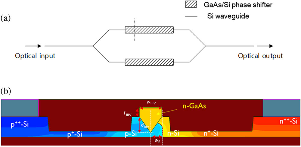
Figure 1.(a) Schematic of a Mach–Zehnder modulator with the III–V/Si optical phase shifters in both arms. (b) Cross-section of the GaAs/Si optical phase shifter.
The device was fabricated by IMEC’s CMOS line, including the monolithic selective area growth of the GaAs on the V-grooved Si trenches fabricated on a 300 mm Si-on-insulator substrate (SOI, top
![]()
Figure 2.Integration flow of the GaAs/Si optical phase shifter. (a) Si-on-insulator, (b) waveguide formation, (c) L-shape pn junction formation, (d) Si V-groove formation, (e) epitaxial GaAs growth on Si V-groove, (f) planarization, and (g)
To investigate the layer quality of the grown n-GaAs film, we investigated the structural quality by scanning transmission electron microscopy (STEM). Figures 3(a) and 3(b) show the dark-field (DF) STEM image of the device cross-section and magnified image of the waveguide core, respectively. The GaAs/Si interface is clearly shown in Fig. 3(b). The bright image contrast indicates the presence of misfit dislocation in the DF-STEM picture.
![]()
Figure 3.(a) Cross-section of the optical phase shifter and (b) the magnified dashed yellow rectangle for GaAs/Si V-groove.
It was reported before in Ref. [20] that under our chosen GaAs growth conditions a periodic array of 60° misfit dislocations is initiated along the two {111} GaAs/Si interfaces of the V-groove. This misfit array ensures the main strain relaxation and causes very bright contrast lines in the DF-STEM image. Residual strain inside the GaAs ridge leads to the nucleation of additional threading dislocations, which are also visible in the main GaAs ridge material as white contrast lines. The density of these threading dislocations clearly reduces going from the GaAs/Si interface to the GaAs ridge surface. Therefore, the crystal quality near the interface is worse than that of the top region. Figure 4 shows the energy dispersive X-ray spectroscopy (EDX) results of the GaAs on the Si V-groove region. The two-dimensional profiles of the Si, Ga, and As atoms are shown in Figs. 4(a), 4(b), and 4(c), respectively. As expected from the DF-STEM image in Fig. 3, the EDX images also show the clearly divided regions for Si and GaAs.
![]()
Figure 4.EDX images of (a) Si, (b) Ga, and (c) As.
3. DEVICE CHARACTERISTICS
Figure 5 shows a microscopic top-view image of the fabricated lumped MZ modulators with GaAs/Si optical phase shifters. The three MZMs consist of grating couplers at the edges of both sides, two asymmetric arms with a 40-μm-length difference, optical phase shifters in both arms with three different lengths of 500, 1000, and 1500 μm, and electrodes on highly doped Si regions for both arms.
![]()
Figure 5.Optical microscopic top-view image of the fabricated GaAs/Si V-groove lumped MZ modulators of 500-, 1000-, and 1500-μm-long optical phase shifters at both arms.
We evaluated the electrical characteristics of the pn junctions in the GaAs/Si and Si optical phase shifters. The Si optical phase shifter was also characterized as a reference, which was simultaneously fabricated on the same wafer. It has a typical lateral pn junction without a V-groove and GaAs on the Si rib waveguide. Figure 6(a) shows the current-voltage (
![]()
Figure 6.Electrical characteristics of the pn junction in the GaAs/Si and Si optical phase shifters: (a) current-voltage and (b) capacitance-voltage.
For electro-optic characteristics, we measured the transmission of both lumped MZ modulators, applying the DC bias voltages shown in Fig. 7. In Fig. 5, continuous-wave transverse magnetic (TE)-polarized light in the wavelength range of 1530–1580 nm was coupled to the grating coupler on the wafer through a cleaved optical fiber. Then, the output power was measured similarly at the different bias points of the forward bias (0.5 V to the reversed bias,
![]()
Figure 7.Bias-dependent measured spectra of the lumped MZ modulators with the 500-μm-phase shifter length: (a) the Si reference and (b) the GaAs/Si.
The wavelength spectra shifted with the increasing bias voltage, resulting in the increase of the optical phase difference between the two Mach–Zehnder interferometer (MZI) arms due to the plasma dispersion effect. Notably, the GaAs/Si device shows a much larger spectrum shift than the Si pn device, indicating a much efficient phase shift at the same bias conditions, which is attributed to the stronger free-electron effects in the n-GaAs. On the other hand, as seen in the spectra between the REF waveguide and MZ modulators, the insertion loss of the GaAs/Si modulator is slightly higher than that of the Si reference modulator by the difference between the spectra of the REF waveguide and the MZ modulators. We will discuss the main causes later, which are the two possible losses from the phase shifter and waveguide transitions from the Si to the GaAs/Si waveguide.
For quantitative analysis, the phase shift was extracted from these shifts in the spectra. Figure 8 shows the extracted optical phase shift and modulation efficiency of
![]()
Figure 8.(a) Extracted phase shift and (b)
To characterize the phase shifter loss, we measured the transmission spectra of the MZ modulators with three different phase shifter lengths, 500, 1000, and 1500 μm, to estimate a propagation loss of an optical phase shifter. Figures 9(a) and 9(b) show the spectra for Si and GaAs/Si, respectively. The transmissions show clear interference patterns and power dependency on the lengths. By increasing the length, the insertion loss increases due to the optical loss in the phase shifter. The increase in the insertion loss of the GaAs/Si device is larger than that in the Si device, indicating higher propagation loss of the GaAs/Si compared to the Si.
![]()
Figure 9.Phase shifter length-dependent measured spectra of the lumped MZ modulators with 500-, 1000-, and 1500-μm phase shifter lengths: (a) the Si reference and (b) the GaAs/Si.
The propagation loss was extracted from the slope of the normalized insertion loss as a function of the length, as shown in Fig. 10. Here, the normalized insertion loss is given by the difference between transmissions at 1550 nm of the Si REF waveguide and the MZMs. The extracted propagation losses are 6.46 dB/mm for the GaAs/Si and 4.54 dB/mm for the Si, respectively. Since the amount of the implantation dose in the pn junction formation was larger than in the conventional Si optical phase shifter (
To extract the waveguide transition loss, we measured the test site including a reference waveguide (REF waveguide) and spiral waveguides (Spiral 01 and Spiral 02), as shown in Fig. 8(a). In Spiral 01 and Spiral 02, the GaAs/Si waveguides are included, and one of them is indicated by a red-colored rectangle. Here, the GaAs/Si waveguide is the same as the GaAs/Si V-groove phase shifter, but the Si is not doped the same as the phase shifter, indicating no free-carrier absorption induced optical loss due to the boron and phosphorus implantation like the phase shifter. The enlarged image of Fig. 11(a) is shown in Fig. 11(b). As it can be seen, the GaAs/Si waveguide is included. Figure 11(c) shows the waveguide transition from Si to GaAs/Si waveguides, which is the blue-colored part in Fig. 11(b). It consists of the 8-μm-long discrete taper. Figure 11(d) is the measured transmission of the three waveguides. The insertion loss (IL) and the transmission difference between the REF and the spiral waveguides, IL(01) and IL(02) in the figure, can be expressed as
Parameter Values of Waveguide Lengths and Number of Waveguide Transitions for Spiral 01 and Spiral 02
| Spiral 01 | 1561 | 6439 | 36 |
| Spiral 02 | 9990 | 5010 | 36 |
![]()
Figure 10.Normalized insertion as a function of the phase shifter length for extracting the propagation loss of the GaAs/Si and the Si reference phase shifters.
![]()
Figure 11.(a) Test site of the spiral waveguides including the GaAs/Si waveguide, the Si waveguide, and the waveguide transition. (b) The GaAs/Si waveguide region, red-colored rectangle. (c) The waveguide transition region from the Si to the GaAs/Si waveguide, blue-colored rectangle. (d) The measured transmission of the REF waveguide, Spiral 01, and Spiral 02.
![]()
Figure 12.(a) Propagation loss of the GaAs/Si waveguide and (b) the insertion loss of the waveguide transition.
To estimate the performance of the optical modulator, the optical modulation amplitude (OMA) is an important parameter, considering both parameters of the
![]()
Figure 13.(a) Optical power versus applied voltage for the OMA definition and (b) the comparison of the OMA versus the phase shifter length between the GaAs/Si and the Si modulators.
4. CONCLUSION
In this paper, we demonstrated monolithically integrated n-GaAs/p-Si depletion-type optical phase shifters fabricated on a 300 mm wafer-scale Si photonics platform. We characterized Mach–Zehnder modulators with the GaAs/Si optical phase shifters on both arms. They show
Acknowledgment
Acknowledgment. The EDA tool was supported by the IC Design Education Center (IDEC), Korea.
References
[1] Y. Kim, J.-H. Han, D. Ahn, S. Kim. Heterogeneously-integrated optical phase shifters for next-generation modulators and switches on a silicon photonics platform: a review. Micromachines, 12, 625(2021).
[2] A. Rahim, A. Hermans, B. Wohlfeil, D. Petousi, B. Kuyken, D. van Thourhout, R. G. Baets. Taking silicon photonics modulators to a higher performance level: state-of-the-art and a review of new technologies. Adv. Photon., 3, 024003(2021).
[3] C. Xiong, D. M. Gill, J. E. Proesel, J. S. Orcutt, W. Haensch, W. M. J. Green. Monolithic 56 Gb/s silicon photonic pulse-amplitude modulation transmitter. Optica, 3, 1060-1065(2016).
[4] P. Dong, X. Liu, S. Chandrasekhar, L. L. Buhl, R. Aroca, Y.-K. Chen. Monolithic silicon photonic integrated circuits for compact
[5] T. Thiessen, P. Grosse, J. Da Fonseca, P. Billondeau, B. Szelag, C. Jany, J. K. S. Poon, S. Menezo. 30 GHz heterogeneously integrated capacitive InP-on-Si Mach–Zehnder modulators. Opt. Express, 27, 102-109(2019).
[6] T. Hiraki, T. Aihara, K. Hasebe, K. Takeda, T. Fujii, T. Kakitsuka, T. Tsuchizawa, H. Fukuda, S. Matsuo. Heterogeneously integrated III–V/Si MOS capacitor Mach–Zehnder modulator. Nat. Photonics, 11, 482-485(2017).
[7] T. Hiraki, T. Aihara, T. Fujii, K. Takeda, Y. Maeda, T. Kakitsuka, T. Tsuchizawa, S. Matsuo. Integration of a high-efficiency Mach-Zehnder modulator with a DFB laser using membrane InP-based devices on Si photonics platform. Opt. Express, 29, 2431-2441(2021).
[8] J.-H. Han, F. Boeuf, J. Fujikata, S. Takahashi, S. Takagi, M. Takenaka. Efficient low-loss InGaAsP/Si hybrid MOS optical modulator. Nat. Photonics, 11, 486-490(2017).
[9] Q. Li, J.-H. Han, C. P. Ho, S. Takagi, M. Takenaka. Ultra-power-efficient 2 × 2 Si Mach-Zehnder interferometer optical switch based on III–V/Si hybrid MOS phase shifter. Opt. Express, 26, 35003-35012(2018).
[10] Q. Li, C. P. Ho, S. Takagi, M. Takenaka. Optical phase modulators based on reverse-biased III-V/Si hybrid metal-oxide-semiconductor capacitors. IEEE Photon. Technol. Lett., 32, 345-348(2020).
[11] M. Takenaka, J.-H. Han, F. Boeuf, J.-K. Park, Q. Li, C. P. Ho, D. Lyu, S. Ohno, J. Fujikata, S. Takahashi, S. Takagi. III–V/Si hybrid MOS optical phase shifter for Si photonic integrated circuits. J. Lightwave Technol., 37, 1474-1483(2019).
[12] B. R. Bennett, R. A. Soref, J. A. Del Alamo. Carrier-induced change in refractive index of InP, GaAs and InGaAsP. IEEE J. Quantum Electron., 26, 113-122(1990).
[13] N. Waldron, C. Merckling, L. Teugels, P. Ong, S. A. U. Ibrahim, F. Sebaai, A. Pourghaderi, K. Barla, N. Collaert, A. V.-Y. Thean. InGaAs gate-all-around nanowire devices on 300 mm Si substrates. IEEE Electron Device Lett., 35, 1097-1099(2014).
[14] C. I. Ozdemir, Y. De Koninck, D. Yudistira, N. Kuznetsova, M. Baryshnikova, D. Van Thourhout, B. Kunert, M. Pantouvaki, J. Van Campenhout. Low dark current and high responsivity 1020 nm InGaAs/GaAs nano-ridge waveguide photodetector monolithically integrated on a 300-mm Si wafer. J. Lightwave Technol., 39, 5263-5269(2021).
[15] Z. Wang, B. Tian, M. Pantouvaki, W. Guo, P. Absil, J. Van Campenhout, C. Merckling, D. Van Thourhout. Room-temperature InP distributed feedback laser array directly grown on silicon. Nat. Photonics, 9, 837-842(2015).
[16] Y. Shi, Z. Wang, J. Van Campenhout, M. Pantouvaki, B. Kunert, D. Van Thourhout. Monolithic InGaAs/GaAs multi-QWs DFB nanoridge laser directly grown on 300 mm Si wafer. Advanced Photonics 2017, ITu2A.2(2017).
[17] Y. Kim, S.-H. Kim, Y. Ban, S. Lardenois, D. Yudistira, M. Pantouvaki, J. Van Campenhout. Proposal and simulation of a low loss, highly efficient monolithic III–V/Si optical phase shifter. 16th International Conference on Group IV Photonics (GFP), WP29(2019).
[18] S. Kim, Y. Kim, Y. Ban, M. Pantouvaki, J. Van Campenhout. Simulation study of a monolithic III-V/Si V-groove carrier depletion optical phase shifter. IEEE J. Quantum Electron., 56, 6300208(2020).
[19] M. Paladugu, C. Merckling, R. Loo, O. Richard, H. Bender, J. Dekoster, W. Vandervorst, M. Caymax, M. Heyns. Site selective integration of III–V materials on Si for nanoscale logic and photonic devices. Cryst. Growth Des., 12, 4696-4702(2012).
[20] W. Guo, Y. Mols, J. Belz, A. Beyer, K. Volz, A. Schulze, R. Langer, B. Kunert. Anisotropic relaxation behavior of InGaAs/GaAs selectively grown in narrow trenches on (001) Si substrates. J. Appl. Phys., 122, 025303(2017).
[21] A. Georgakilas, E. Aperathitis, V. Foukaraki, M. Kayambaki, P. Panayotatos. Investigation of the GaAs/Si heterojunction band lineup with capacitance and current versus voltage measurements. Mater. Sci. Eng. B, 44, 383-386(1997).
[22] G. Wang, G. Y. Zhao, T. Soga, T. Jimbo, M. Umeno. Effects of H plasma passivation on the optical and electrical properties of GaAs-on-Si. Jpn. J. Appl. Phys., 37, L1280-L1282(1998).
[23] G. Wang, T. Ogawa, T. Soga, T. Jimbo, M. Umeno. Detailed study of H2 plasma passivation effects on GaAs/Si solar cell. Sol. Energy Mater. Sol. Cells, 66, 599-605(2001).
[24] K. C. Hsieh, M. S. Feng, G. E. Stillman, N. Holonyak, C. R. Ito, M. Feng. Hydrogenation and subsequent hydrogen annealing of GaAs on Si. Appl. Phys. Lett., 54, 341-343(1989).
[25] S. J. Pearton, C. S. Wu, M. Stavola, F. Ren, J. Lopata, W. C. Dautremont-Smith, S. M. Vernon, V. E. Haven. Hydrogenation of GaAs on Si: effects on diode reverse leakage current. Appl. Phys. Lett., 51, 496-498(1987).
[26] V. Swaminathan. Defects in GaAs. Bull. Mater. Sci., 4, 403-442(1982).
[27] M. R. Watts, W. A. Zortman, D. C. Trotter, R. W. Young, A. L. Lentine. Low-voltage, compact, depletion-mode, silicon Mach–Zehnder modulator. IEEE J. Sel. Top. Quantum Electron., 16, 159-164(2010).
[28] Y. Kim, T. Jin, Y. Bae. A comparative simulation study on lateral and L-shape pn junction phase shifters for single-drive 50 Gbps lumped Mach-Zehnder modulators. Jpn. J. Appl. Phys., 60, 052002(2021).
[29] E. Peiner, A. Guttzeit, H.-H. Wehmann. The effect of threading disclocations on optical absorption and electron scattering in strongly mismatched heteroepitaxial III–V compound semiconductors on silicon. J. Phys. Condens. Matter, 14, 13195-13201(2002).
[30] F. Boeuf, J.-H. Han, S. Takagi, M. Takenaka. Benchmarking Si, SiGe, and III–V/Si hybrid SIS optical modulators for datacenter applications. J. Lightwave Technol., 35, 4047-4055(2017).
[31] D. A. B. Miller. Energy consumption in optical modulators for interconnects. Opt. Express, 20, A293-A308(2012).


Set citation alerts for the article
Please enter your email address

© Copyright 2018-2021 | Chinese Laser Press. All Rights Reserved 沪ICP备15018463号-20