
Jiachen Li, Sigang Yang, Hongwei Chen, Xingjun Wang, Minghua Chen, Weiwen Zou, "Fully integrated hybrid microwave photonic receiver," Photonics Res. 10, 1472 (2022)
- Photonics Research
- Vol. 10, Issue 6, 1472 (2022)
Abstract
1. INTRODUCTION
Microwave photonics (MWP) is a promising interdisciplinary technology positioned so as to overcome the performance bottleneck of traditional microwave systems by utilizing the inherent superiorities of photonic technologies [1,2], including wide operation bandwidth, low loss, flexibility, and immunity to electromagnetic interference. Leveraging these unique advantages, the MWP has propelled technological advancements in plenty of radio-frequency (RF) applications, such as microwave photonic filters [3–7], photonic analog-to-digital converters (ADCs) [8,9], microwave photonic receivers (transmitters) [10–17], photonics-based microwave generation [18–21], photonics-based microwave measurement [22,23], transport and distribution of RF signals over optical fiber (ROF) [24,25], and photonic true-time delay beamforming [26–28]. Particularly recently, driven by urgent requirements on size, weight, and power consumption (SWaP) oriented to miniaturized application scenarios and the technological maturity of photonic integrated circuits (PICs), researchers have been attempting to shift more efforts from the validation of system concepts based on bulk optical components to the implementation of MWP microsystems based on PICs, widely known as integrated microwave photonics (IMWP) [29,30].
A long-standing goal of IMWP is to demonstrate chip-scale microsystems with all the required active and passive optoelectronic components integrated into the same substrate, either monolithically [3,20] or through hybrid integration approaches [5,27]. Most of the recent IMWP demonstrations have been based on three mainstream photonic integrated platforms [29]: indium phosphide (InP) [31,32], silicon nitride (
Fortunately, heterogeneous or hybrid integration of III–V materials with SOI or
Sign up for Photonics Research TOC. Get the latest issue of Photonics Research delivered right to you!Sign up now
In this work, we report for the first time, to the best of our knowledge, a chip-scale fully integrated hybrid microwave photonic receiver (FIH-MWPR) with the integration of all optoelectronic components, including the laser source, high-speed phase modulators, tunable optical bandpass filters based on microring resonators (MRRs), and photodetectors. Here, all the functionalities except the laser source are monolithically integrated on an SOI PIC, whereas the light is provided by an InP distributed feedback (DFB) semiconductor laser chip. These two complementary platforms are hybrid integrated into the same substrate with the method of free-space micro-optics. Figure 1 presents the photograph of the completely packaged FIH-MWPR module, occupying a compact volume of
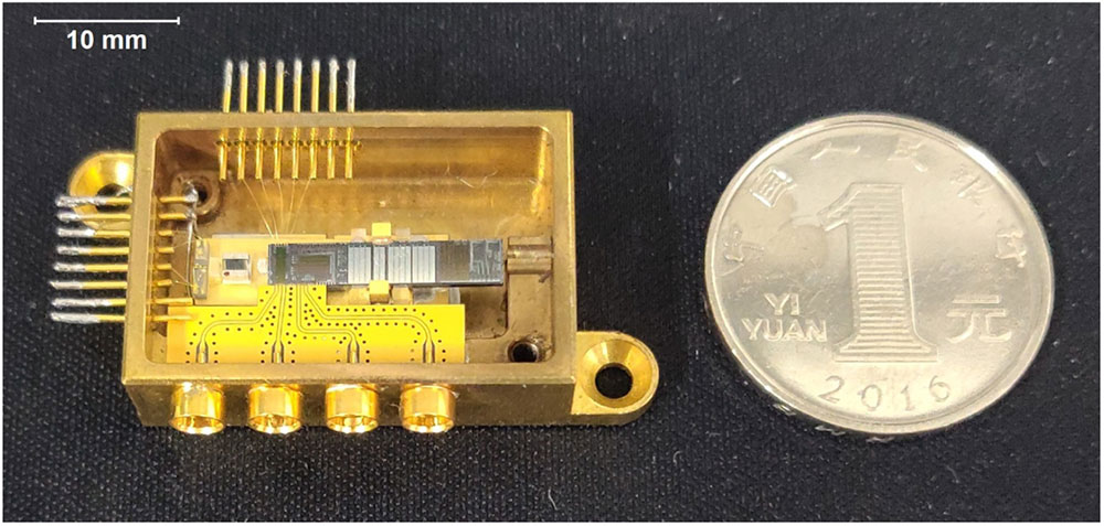
Figure 1.Packaged FIH-MWPR module with a compact volume of
2. FIH-MWPR ARCHITECTURE AND CHIP DESIGN
Figure 2(a) illustrates the schematic architecture of the proposed FIH-MWPR, where an InP-based DFB laser chip and a monolithic SOI-based PIC are hybrid-integrated through the micro-optics-based approach to establish a complete IMWP microsystem. The SOI-based PIC includes most of the required on-chip optoelectronic components: two parallel high-speed phase modulators, two tunable optical bandpass filters based on MRRs, and a photodetector array. The operation principle of this FIH-MWPR is presented by describing the evolution of optical and electrical spectra at several key points labeled in the system, as shown in Fig. 2(b). A continuous-wave light around 1550 nm provided by the InP-based DFB laser chip first goes through a sub-assembly comprising two microlenses and a micro-isolator and is coupled into the SOI PIC via an on-chip spot-size converter. Then the light is split equally into two branches as optical carriers by a 50:50 multimode interferometer (MMI). The optical carrier in the upper branch is sent into a high-speed phase modulator, which is driven by the received RF input signal, while the optical carrier in the lower branch is sent into another parallel phase modulator, which is driven by the RF local oscillator (LO). Here, we choose the phase modulator instead of the Mach–Zehnder modulator (MZM) because of its good linearity and no extra phase bias [10]. The modulated optical signals leaving the phase modulators are then routed to MRR-based tunable optical bandpass filters for the signal extracting. The target RF signal and LO are selected from their first-order modulation sidebands, respectively. Finally, these extracted signals from the filters are mixed by a 50:50 optical coupler and sent into photodetectors for down-converting the target RF signal to the intermediate frequency (IF), which equals the beat difference between frequencies of the target RF signal and LO. Owing to the employed tunable optical bandpass filters, the FIH-MWPR can flexibly select the target part from the modulated broadband RF input signal in the optical domain, which substantially lightens the burden of broadband signal processing in the RF domain. Meanwhile, the instantaneous bandwidth of the FIH-MWPR is basically determined by the passband width of employed optical bandpass filters.
![]()
Figure 2.(a) Schematic diagram of the proposed FIH-MWPR. DFB, distributed feedback semiconductor laser; SSC, spot-size converter; PM, phase modulator; MRR, microring resonator; PD, photodetector. (b) Spectra at several key points labeled in the system. 1, 2, and 3 are optical spectra, and 4 is the electrical spectrum. The signal–signal beat interference (SSBI) at 4 is ignored. (c) Optical microscope images of key elements on the fabricated SOI chip. (d) Cross-sectional schematic view (not to scale) of the SOI platform.
The monolithic SOI PIC is fabricated on a standard 220 nm SOI platform based on CMOS-compatible processes offered by Advanced Micro Foundry (AMF) [37]. The footprint of the whole chip is
The employed InP-based semiconductor laser chip is a commercially available large-power narrow-linewidth DFB laser diode capable of providing a single-mode output light of 50 mW near 1550 nm under a typical injection current of 200 mA. With the method of micro-optics, the coupling loss between the InP DFB laser chip and the SOI PIC is optimized at about 3.5 dB, and a 1 dB loss here is induced by the polarization-maintaining micro-isolator (50 dB isolation) inserted between two microlenses. This micro-isolator is necessary to protect the laser chip from the feedback light reflected back from the SOI PIC [67].
These two chips and micro-optic components are mounted on a W-Cu submount with an underneath thermo-electric cooler (TEC) controlled by a high-resolution temperature controller (Arroyo Instruments, 5305 TECSource, the long-term stability is 0.01°C over 24 h), and assembled into a compact package, as shown in Fig. 1. Moreover, the RF signals applied to modulators and the IF signals generated by photodetectors are carried from on-chip RF pads to the SMP connectors on the package through wire bonding and custom-designed RF transmission lines mounted on ceramics.
3. EXPERIMENTAL RESULTS
A. Characterization of Key Elements
On-chip SOI phase modulators in the FIH-MWPR are critical elements for up-converting the RF signals to the optical domain, ultimately determining the operation bandwidth of the microsystem. We experimentally characterize the electro-optic (E/O) modulation responses by measuring the optical modulation spectrum from the grating coupler and recording the first-order modulation sideband power under different driving frequencies and bias voltages, using a high-resolution optical spectrum analyzer (OSA, APEX, AP2081B). Figure 3 shows the measured E/O modulation responses of the phase modulator with or without the package. For the unpackaged on-chip phase modulator, we utilize a 40 GHz probe (GGB, 40A-GSG-150-LP) to load the RF driving signal onto the pad. In this case, the measured response is mainly decided by the on-chip modulator itself. As shown in Fig. 3(a), the on-chip phase modulator supports an intrinsic 3 dB E/O bandwidth of 10 GHz at 0 V bias, which gradually increases to
![]()
Figure 3.Normalized measured E/O modulation responses of (a) the unpackaged on-chip phase modulator and (b) the packaged phase modulator under various bias voltages.
We further evaluate the half-wave voltage (
On-chip MRR-based tunable bandpass filters are utilized to extract the target signal from the modulation sidebands in the optical domain, and their tunability ensures the software-defined flexibility of the FIH-MWPR across the whole operation frequency band. We experimentally characterize the transmission responses of MRR filters using the aforementioned OSA with a built-in tunable laser. Figure 4(a) depicts the directly measured notch response spectrum (green, dots) of the MRR from the grating coupler. By fitting this measured notch response to the theoretical Lorentzian transfer function (green, dashed line) of add-drop MRRs [69], we extract key parameters of the MRR and simulate its corresponding bandpass response (blue, solid line), which exhibits a 3 dB bandwidth of 4.74 GHz and an insertion loss of
![]()
Figure 4.(a) Measured MRR notch response (green, dots), simulated MRR bandpass response (blue, solid line), and the Lorentzian fitting (green, dashed line) of the measured notch response. (b) The MRR resonance wavelength is tuned with the increasing heating power. (c) Temporal waveform of the square-wave electrical driving signal applied on the TiN microheater. (d) Measured temporal optical response with a fall/rise time of
On-chip photodetectors are utilized to down-convert the processed modulated signals from the optical back to the electrical domain. Figure 5(a) shows the measured photocurrent as a function of the input optical power at the wavelength of 1550 nm under different bias voltages. The responsivity of the photodetector is measured to be 1.02 A/W at a bias voltage of
![]()
Figure 5.(a) Measured responsivities of on-chip photodetectors under various bias voltages. (b) Normalized measured O/E responses of on-chip photodetectors under various bias voltages.
The InP-based large-power DFB semiconductor laser chip in the FIH-MWPR provides an optical carrier at
![]()
Figure 6.(a) Measured optical spectrum of the employed InP-based DFB semiconductor laser. (b) Frequency noise measurement of the DFB laser showing a Lorentzian linewidth of
B. RF-link Performance Metrics
The RF-link performance metrics, including the link gain, the NF, and the SFDR, quantitatively characterize the system performance of the demonstrated FIH-MWPR module to down-convert the RF signals to the IF, and these metrics are measured using the standard two-tone test [4]. As a specific example, a two-tone test signal (14.001 and 13.999 GHz) generated by a vector signal generator (Agilent E8267D) drives the RF signal modulator, while another single-tone signal (14.2 GHz, 20 dBm) generated by an analog signal generator (Anritsu, MG3694B) drives the LO modulator. After the operation presented in Section 2, the FIH-MWPR module down-converts the two-tone RF input signal to IF at 0.199 and 0.201 GHz, as shown by the electrical spectrum in Fig. 7(a), which is acquired by an electrical spectrum analyzer (ESA, Agilent, N9030A). However, due to nonlinearities induced in the modulation and photodetection, the third-order intermodulation distortion (IMD3) tones (0.197 and 0.203 GHz) arise close to the desired IF fundamental tones, which are regarded as the pivotal distortion limiting the linear dynamic range of the FIH-MWPR, since the second-order intermodulation distortion (IMD2) can be easily filtered out in the electrical domain for common narrowband signals [30]. Furthermore, we measure the output power of IF fundamental tones and IMD3 tones under different RF input power in this case, as shown in Fig. 7(b). Here, by calculating the power ratio of IF fundamental tones to the RF input signal, the link gain (G) is extracted to be
![]()
Figure 7.(a) Measured electrical spectrum (RBW: 100 kHz, VBW: 1 kHz) of the down-converted IF signal, with the two-tone RF signal centered at 14 GHz (14.001 and 13.999 GHz) and the LO (20 dBm) centered at 14.2 GHz. (b) Measured output power of the IF fundamental tones and the IMD3 tones under different RF input power. (c) Measured link gain of the FIH-MWPR over the frequency range from 2 to 18 GHz. (d) Measured noise floor of the FIH-MWPR over the frequency range from 2 to 18 GHz. (e) Measured NF of the FIH-MWPR over the frequency range from 2 to 18 GHz. (f) Measured SFDR of the FIH-MWPR over the frequency range from 2 to 18 GHz.
We further performed the aforementioned two-tone test to measure the RF-link performance metrics of the FIH-MWPR across the whole operation frequency band, with the RF input frequency varying from 2 to 18 GHz and the corresponding LO varying from 2.2 to 18.2 GHz. Figures 7(c)–7(f) show the measured link gain, noise floor, NF, and SFDR as functions of the RF input frequency, respectively. The link gain reaches a maximum of
To further characterize the capability of the FIH-MWPR to down-convert the RF input signal to different intermediate frequencies, we measure the RF-link performance metrics by gradually tuning the LO frequency from 14.1 to 17 GHz and fixing the RF input frequency at 14 GHz. As shown by the link gain, NF, and SFDR measured as functions of the IF in Fig. 8, the FIH-MWPR is verified to maintain a stable performance with the IF ranging from 0.1 to 3 GHz. Here, the slight variation of measured RF-link performance metrics is attributed to the nonuniform frequency responses of phase modulators and photodetectors under different operation frequencies, as shown in Figs. 3 and 5.
![]()
Figure 8.Link gain, NF, and SFDR measured as functions of IF. Here, the RF input signal is fixed at 14 GHz, while the LO (20 dBm) is tuned from 14.1 to 17 GHz.
The measured RF-link performance metrics of the demonstrated FIH-MWPR are consistent with predicted values and comparable to those of reported integrated systems with equivalent external optical input. For instance, in Ref. [15], our research group has once proposed an SOI-based microwave photonic transceiver with an external laser source and experimentally demonstrated its down-conversion function, which exhibits a link gain of
C. System Performance Evaluation as a De-chirp Receiver
In this part, we evaluate the system performance of the demonstrated FIH-MWPR as a de-chirp receiver for processing broadband LFM radar echo signals at different frequency bands (S-, C-, X-, and Ku-bands) by utilizing the fiber-delay-based radar target emulator, where the electrical LFM radar signal is up-converted to the optical domain and delayed in an optical fiber spool. The experimental setup is shown in Fig. 9(a). A continuous-wave optical carrier is provided by a narrow-linewidth fiber laser source (NKT Photonics, Adjustik E15) and then modulated by an MZM (EOSPACE, 20 GHz). The MZM is driven by the LFM signal generated by a high-speed arbitrary waveform generator (AWG, Tektronix AWG70001A) with a sampling rate of 50 GSa/s. The modulated optical signal is amplified by an erbium-doped fiber amplifier (EDFA), followed by an optical bandpass filter to eliminate the amplified spontaneous emission (ASE) noise. Then the light is equally split into two branches by an optical coupler. In the lower branch, the light is directly sent into a photodetector (Finisar XPDV2120R) to obtain the down-converted LFM signal from the optical back to the electrical domain, with a variable optical attenuator (VOA) inserted to adjust the signal power. The electrical LFM signal is then amplified by a low-noise amplifier (LNA) and filtered by an electrical bandpass filter. Unlike the lower branch, the light in the upper branch is first delayed in an optical fiber spool before being sent into the photodetector, and thus the time delay between two branches is determined by the length of the employed optical fiber spool. Here, the delayed electrical LFM signal from the upper branch is used as the emulated radar echo signal, while that from the lower branch is used as the LO for de-chirping the radar echo. The echo signal and LO are then sent into the demonstrated FIH-MWPR and processed as the operation stated in Section 2. Subsequently, the de-chirped IF signal generated by the FIH-MWPR is acquired by a low-speed ADC module (2 GSa/s) and processed by a digital signal processor (DSP). The de-chirping principle is illustrated in the inset of Fig. 9(a). In the case of fiber-delay-based radar target emulator, assuming the fiber delay length between two branches is
![]()
Figure 9.(a) Experimental setup for evaluating the system performance of the FIH-MWPR as a de-chirp receiver. The inset shows the de-chirping principle. MZM, Mach–Zehnder modulator; EDFA, erbium-doped fiber amplifier; OBPF, optical bandpass filter; OC, optical coupler; VOA, variable optical attenuator; PD, photodetector; AWG, arbitrary waveform generator; LNA, low noise amplifier; EBPF, electrical bandpass filter; ADC, analog to digital converter; DSP, digital signal processor. (b) Instantaneous time-frequency diagrams of generated LFM radar echo signals from the fiber-delay-based radar target emulator at different frequency bands (S-, C-, X-, and Ku-bands). (c) The normalized electrical spectra of de-chirped IF signals generated by the FIH-MWPR, with the LFM radar signals located at different frequency bands (S-, C-, X-, and Ku-bands). The insets show the zoom-in views around the main peaks. (d) Measured frequencies of the de-chirped IF signals under different fiber delay distances, with the LFM radar signals located at different frequency bands (S-, C-, X-, and Ku-bands).
Figure 9(b) shows instantaneous time-frequency diagrams of emulated radar echo signals covering different bandwidths at S-, C-, X-, and Ku-bands, which are calculated based on the short-time Fourier transform (STFT) of temporal waveforms acquired using a 50 GSa/s digital oscilloscope (Tektronix, DPO72004B). In our experimental setup, the fiber delay length of the radar echo signal in the fiber-delay-based radar target emulator is set at
Normalized electrical spectra of de-chirped IF signals generated by the FIH-MWPR are obtained by performing the fast Fourier transform (FFT) on the captured waveforms from the ADC and plotted in Fig. 9(c). With the LFM radar signal covering a bandwidth of 2 GHz in the S-band (2–4 GHz), the de-chirped IF signal shows a low-frequency main peak at 100.901 MHz, indicating a fiber delay length of
We further evaluate the range measurement accuracy of the FIH-MWPR as a de-chirp receiver by gradually increasing the fiber delay distance with fiber patch cords. Here, the employed fiber patch cords are accurately calibrated using a commercial high-resolution optical vector network analyzer (LUNA, OVA5000) with a detection resolution of 1 mm. Figure 9(d) shows measured frequencies of the de-chirped IF signals under the increasing fiber delay distance, with the LFM radar signals at different frequency bands. For example, when the FIH-MWPR operates at S-band with the LFM radar signal covering a bandwidth of 2 GHz, the measured frequencies of de-chirped IF signals agree well with theoretical values calculated based on Eq. (3). As can be seen, the measured frequency errors are kept within
4. DISCUSSION
We compare our work with the state-of-the-art integrated microwave photonic receivers, and their overall performance is summarized in Table 1. Compared to the work in Ref. [11], which relies on hybrid integrating unpackaged discrete components (laser, crystal modulators, fiber filters, and PDs) into a common enclosure, our FIH-MWPR features a significant reduction in SWaP by further integrating all functional components into the chip. Here, the power consumption of the demonstrated FIH-MWPR is estimated to be only about 1.2 W, which mainly originates from the laser diode driver (
Comparison among Reported Integrated Microwave Photonic Receivers [
| Platforms | Configuration and | Volume | Power | Operation | Link | NF | SFDR |
|---|---|---|---|---|---|---|---|
| Hybrid III-V/SOI (this work) | All components (laser, modulators, filters, and PDs) are on-chip and hybrid integrated. | 6 | 1.2 | 2–18 | −51.9 to −58.6 | 59.7–75.2 | 89.0–94.1 |
| Hybrid III- | Unpackaged laser, crystal modulators, fiber filters, and PDs are hybrid integrated into a common enclosure. | 180 | 5 | 10–18 | 105 (at 12 GHz) | ||
| SOI [ | Modulators, filters, and PDs are on-chip. The laser is from an external device. | N/A | N/A | 2–10 | 91.9 (at 3 GHz) | ||
| SOI [ | Modulators and PDs are on-chip. The laser is from an external device. No optical filters. | N/A | N/A | 3.4–14.1 | N/A | 99 (at 10.4 GHz) |
N/A, not applicable.
The RF-link performance metrics are evaluated without IF amplifiers.
Among all the integrated microwave photonic receivers listed in Table 1, the FIH-MWPR features the broadest operation bandwidth (2–18 GHz), which mainly benefits from the high-speed modulation performance of on-chip SOI modulators and optimized RF losses in the package (see Fig. 3). Meanwhile, thanks to the broadband tunability and the fast tuning speed of on-chip bandpass filters (see Fig. 4), the FIH-MWPR can be rapidly switched among different operation frequency bands. In particular, to further validate the broadband processing capability of the FIH-MWPR toward real-world application scenarios, we utilized it as a de-chirp receiver to process the broadband LFM radar echo signals at different frequency bands (S-, C-, X-, and Ku-bands). With the optimized traveling-wave electrode structure and well-designed doping profile, the 3 dB E/O bandwidth of the silicon modulator can be improved to 40 GHz after packaging [74,75]. Besides, with the improved doping structure, the O/E bandwidth of the Ge-on-Si photodetector can be increased to over 50 GHz [76]. Therefore, in the future, the operation bandwidth of the FIH-MWPR can be further extended to cover the full K-band and Ka-band.
The RF-link performance metrics of the FIH-MWPR are comparable to those of reported integrated microwave photonic receivers listed in Table 1. However, they still can not compete with those of state-of-the-art discrete systems [12,72]. For example, our research group has once proposed an all-optical full-band microwave photonic receiver [12] and conceptually verified its performance based on bulk optical devices. In the experiment, its system performance is measured from
In the FIH-MWPR, the optical bandpass filters process the modulated microwave photonic signals and determine the instantaneous bandwidth of the receiver. For the employed MRR filters, their out-of-band suppression is limited by the Lorentzian response lineshape, and their filter responses lack reconfigurability toward different application scenarios. To further improve the receiver performance, the more complex filter based on the lattice structure [77] could be considered in the future. For example, based on three-stage cascaded ring-assisted Mach–Zehnder interferometers (RAMZIs), the optical rectangular filter shows a continuously tunable bandwidth from 4.1 to 14.1 GHz and a good shape factor [78]. Therefore, by substituting this reconfigurable rectangular filter for the MRR filter, we can realize a reconfigurable microwave photonic receiver with a tunable instantaneous bandwidth toward different application scenarios.
5. CONCLUSIONS
In conclusion, we presented here, to the best of our knowledge, the first realization of a chip-scale fully integrated microwave photonic receiver, based on the hybrid integration of the InP laser chip and the SOI PIC. The FIH-MWPR can support a broad operation bandwidth of 2–18 GHz with an instantaneous bandwidth of
Acknowledgment
Acknowledgment. The authors thank Advanced Micro Foundry (AMF) for offering the SOI waveguide manufacturing technology.
References
[1] J. Capmany, D. Novak. Microwave photonics combines two worlds. Nat. Photonics, 1, 319-330(2007).
[2] J. Yao. Microwave photonics. J. Lightwave Technol., 27, 314-335(2009).
[3] S. J. Fandiño, P. Muñoz, D. Domenech, J. Capmany. A monolithic integrated photonic microwave filter. Nat. Photonics, 11, 124-129(2017).
[4] Y. Liu, A. Choudhary, D. Marpaung, B. J. Eggleton. Integrated microwave photonic filters. Adv. Opt. Photon., 12, 485-555(2020).
[5] Y. Tao, H. Shu, X. Wang, M. Jin, Z. Tao, F. Yang, J. Shi, J. Qin. Hybrid-integrated high-performance microwave photonic filter with switchable response. Photon. Res., 9, 1569-1580(2021).
[6] W. Zhang, J. Yao. On-chip silicon photonic integrated frequency-tunable bandpass microwave photonic filter. Opt. Lett., 43, 3622-3625(2018).
[7] Y. Liu, J. Hotten, A. Choudhary, B. J. Eggleton, D. Marpaung. All-optimized integrated RF photonic notch filter. Opt. Lett., 42, 4631-4634(2017).
[8] A. Khilo, S. J. Spector, M. E. Grein, A. H. Nejadmalayeri, C. W. Holzwarth, M. Y. Sander, M. S. Dahlem, M. Y. Peng, M. W. Geis, N. A. DiLello, J. U. Yoon, A. Motamedi, J. S. Orcutt, J. P. Wang, C. M. Sorace-Agaskar, M. A. Popović, J. Sun, G.-R. Zhou, H. Byun, J. Chen, J. L. Hoyt, H. I. Smith, R. J. Ram, M. Perrott, T. M. Lyszczarz, E. P. Ippen, F. X. Kärtner. Photonic ADC: overcoming the bottleneck of electronic jitter. Opt. Express, 20, 4454-4469(2012).
[9] S. Xu, X. Zou, B. Ma, J. Chen, L. Yu, W. Zou. Deep-learning-powered photonic analog-to-digital conversion. Light Sci. Appl., 8, 66(2019).
[10] J. Li, S. Yang, H. Chen, M. Chen. Hybrid microwave photonic receiver based on integrated tunable bandpass filters. Opt. Express, 29, 11084-11093(2021).
[11] A. C. Paolella, R. DeSalvo, C. Middleton, S. Ayotte, M. Morin, G. Bilodeau, L.-P. Perron-Houle, F. Costin, A. Babin, G. Brochu, J. Blanchet-Létourneau, C.-A. Davidson, D. D’Amato, E. Girard-Deschênes, P. Chrétien, M. Laplante, M. Drolet. Hybrid integration of RF photonic systems. J. Lightwave Technol., 36, 5067-5073(2018).
[12] H. Yu, M. Chen, Q. Guo, M. Hoekman, H. Chen, A. Leinse, R. G. Heideman, R. Mateman, S. Yang, S. Xie. All-optical full-band RF receiver based on an integrated ultra-high-
[13] C. Yin, J. Li, L. Shu, Z. Yu, F. Yin, Y. Zhou, Y. Dai, K. Xu. Broadband lower-IF RF receiver based on microwave photonic mixer and Kramers-Kronig detection. Opt. Express, 26, 26400-26410(2018).
[14] W. Chen, D. Zhu, J. Liu, S. Pan. Multi-band RF transceiver based on the polarization multiplexed photonic LOs and mixers. IEEE J. Sel. Top. Quantum Electron., 27, 7601009(2021).
[15] M. Chen, H. Yu, B. Yang, Y. Li, H. Chen, S. Xie. A silicon integrated microwave-photonic transceiver. Optical Fiber Communication Conference, W4B.3(2017).
[16] F. Falconi, S. Melo, F. Scotti, M. N. Malik, M. Scaffardi, C. Porzi, L. Ansalone, P. Ghelfi, A. Bogoni. A combined radar & lidar system based on integrated photonics in silicon-on-insulator. J. Lightwave Technol., 39, 17-23(2021).
[17] S. Li, Z. Cui, X. Ye, J. Feng, Y. Yang, Z. He, R. Cong, D. Zhu, F. Zhang, S. Pan. Chip-based microwave-photonic radar for high-resolution imaging. Laser Photon. Rev., 14, 1900239(2020).
[18] J. Liu, E. Lucas, S. A. Raja, J. He, J. Riemensberger, N. R. Wang, M. Karpov, H. Guo, R. Bouchand, J. T. Kippenberg. Photonic microwave generation in the X- and K-band using integrated soliton microcombs. Nat. Photonics, 14, 486-491(2020).
[19] Y. K. Chembo, D. Brunner, M. Jacquot, L. Larger. Optoelectronic oscillators with time-delayed feedback. Rev. Mod. Phys., 91, 035006(2019).
[20] J. Tang, T. Hao, W. Li, D. Domenech, R. B. Nos, P. M. Noz, N. Zhu, J. Capmany, M. Li. Integrated optoelectronic oscillator. Opt. Express, 26, 12257-12265(2018).
[21] P. Zhou, R. Zhang, N. Li, Z. Jiang, S. Pan. An RF-source-free microwave photonic radar with an optically injected semiconductor laser for high-resolution detection and imaging(2021).
[22] X. Zou, B. Lu, W. Pan, L. Yan, A. Stöhr, J. Yao. Photonics for microwave measurements. Laser Photon. Rev., 10, 711-734(2016).
[23] S. Pan, J. Yao. Photonics-based broadband microwave measurement. J. Lightwave Technol., 35, 3498-3513(2017).
[24] Y. He, K. G. H. Baldwin, B. J. Orr, R. B. Warrington, M. J. Wouters, A. N. Luiten, P. Mirtschin, T. Tzioumis, C. Phillips, J. Stevens, B. Lennon, S. Munting, G. Aben, T. Newlands, T. Rayner. Long-distance telecom-fiber transfer of a radio-frequency reference for radio astronomy. Optica, 5, 138-146(2018).
[25] C. Lim, A. Nirmalathas. Radio-over-fiber technology: present and future. J. Lightwave Technol., 39, 881-888(2021).
[26] C. Zhu, L. Lu, W. Shan, W. Xu, G. Zhou, L. Zhou, J. Chen. Silicon integrated microwave photonic beamformer. Optica, 7, 1162-1170(2020).
[27] C. Tsokos, E. Andrianopoulos, A. Raptakis, N. K. Lyras, L. Gounaridis, P. Groumas, R. B. Timens, I. Visscher, R. Grootjans, L. S. Wefers, D. Geskus, E. Klein, H. Avramopoulos, R. Heideman, C. Kouloumentas, C. G. H. Roeloffzen. True time delay optical beamforming network based on hybrid InP-silicon nitride integration. J. Lightwave Technol., 39, 5845-5854(2021).
[28] X. Xu, J. Wu, T. G. Nguyen, T. Moein, S. T. Chu, B. E. Little, R. Morandotti, A. Mitchell, D. J. Moss. Photonic microwave true time delays for phased array antennas using a 49 GHz FSR integrated optical micro-comb source Invited. Photon. Res., 6, B30-B36(2018).
[29] D. Marpaung, J. Yao, J. Capmany. Integrated microwave photonics. Nat. Photonics, 13, 80-90(2019).
[30] D. Marpaung, C. Roeloffzen, R. Heideman, A. Leinse, S. Sales, J. Capmany. Integrated microwave photonics. Laser Photon. Rev., 7, 506-538(2013).
[31] V. Rustichelli, C. Calò, F. Lemaitre, S. Andreou, N. Michel, F. Pommereau, H. Ambrosius, K. Williams. Monolithic integration of buried-heterostructures in a generic integrated photonic foundry process. IEEE J. Sel. Top. Quantum Electron., 25, 6100808(2019).
[32] G. E. Hoefler, Y. Zhou, M. Anagnosti, A. Bhardwaj, P. Abolghasem, A. James, S. Luna, P. Debackere, A. Dentai, T. Vallaitis, P. Liu, M. Missey, S. Corzine, P. Evans, V. Lal, M. Ziari, D. Welch, F. Kish, J. S. Suelzer, P. S. Devgan, N. G. Usechak. Foundry development of system-on-chip InP-based photonic integrated circuits. IEEE J. Sel. Top. Quantum Electron., 25, 6100317(2019).
[33] P. Muñoz, P. W. L. van Dijk, D. Geuzebroek, M. Geiselmann, C. Domínguez, A. Stassen, J. D. Doménech, M. Zervas, A. Leinse, C. G. H. Roeloffzen, B. Gargallo, R. Baños, J. Fernàndez, G. M. Cabanes, L. A. Bru, D. Pastor. Foundry developments toward silicon nitride photonics from visible to the mid-infrared. IEEE J. Sel. Top. Quantum Electron., 25, 8200513(2019).
[34] C. G. H. Roeloffzen, M. Hoekman, E. J. Klein, L. S. Wevers, R. B. Timens, D. Marchenko, D. Geskus, R. Dekker, A. Alippi, R. Grootjans, A. van Rees, R. M. Oldenbeuving, J. P. Epping, R. G. Heideman, K. Wörhoff, A. Leinse, D. Geuzebroek, E. Schreuder, P. W. L. van Dijk, I. Visscher, C. Taddei, Y. Fan, C. Taballione, Y. Liu, D. Marpaung, L. Zhuang, M. Benelajla, K.-J. Boller. Low-loss Si3N4 TriPleX optical waveguides: technology and applications overview. IEEE J. Sel. Top. Quantum Electron., 24, 4400321(2018).
[35] K. Giewont, K. Nummy, F. A. Anderson, J. Ayala, T. Barwicz, Y. Bian, K. K. Dezfulian, D. M. Gill, T. Houghton, S. Hu, B. Peng, M. Rakowski, S. Rauch, J. C. Rosenberg, A. Sahin, I. Stobert, A. Stricker. 300-mm monolithic silicon photonics foundry technology. IEEE J. Sel. Top. Quantum Electron., 25, 8200611(2019).
[36] T. Aalto, M. Cherchi, M. Harjanne, S. Bhat, P. Heimala, F. Sun, M. Kapulainen, T. Hassinen, T. Vehmas. Open-access 3-μm SOI waveguide platform for dense photonic integrated circuits. IEEE J. Sel. Top. Quantum Electron., 25, 8201109(2019).
[37] S. Y. Siew, B. Li, F. Gao, H. Y. Zheng, W. Zhang, P. Guo, S. W. Xie, A. Song, B. Dong, L. W. Luo, C. Li, X. Luo, G.-Q. Lo. Review of silicon photonics technology and platform development. J. Lightwave Technol., 39, 4374-4389(2021).
[38] W. M. Puckett, K. Liu, N. Chauhan, Q. Zhao, N. Jin, H. Cheng, J. Wu, O. R. Behunin, T. P. Rakich, D. K. Nelson, J. D. Blumenthal. 422 million intrinsic quality factor planar integrated all-waveguide resonator with sub-MHz linewidth. Nat. Commun., 12, 934(2021).
[39] J. Liu, G. Huang, R. N. Wang, J. He, A. S. Raja, T. Liu, N. J. Engelsen, T. J. Kippenberg. High-yield, wafer-scale fabrication of ultralow-loss, dispersion-engineered silicon nitride photonic circuits. Nat. Commun., 12, 2236(2021).
[40] C. Xiang, J. Liu, J. Guo, L. Chang, R. N. Wang, W. Weng, J. Peters, W. Xie, Z. Zhang, J. Riemensberger, J. Selvidge, T. J. Kippenberg, J. E. Bowers. Laser soliton microcombs heterogeneously integrated on silicon. Science, 373, 99-103(2021).
[41] B. Shen, L. Chang, J. Liu, H. Wang, Q.-F. Yang, C. Xiang, N. R. Wang, J. He, T. Liu, W. Xie, J. Guo, D. Kinghorn, L. Wu, Q.-X. Ji, J. T. Kippenberg, K. Vahala, E. J. Bowers. Integrated turnkey soliton microcombs. Nature, 582, 365-369(2020).
[42] B. Stern, X. Ji, Y. Okawachi, A. L. Gaeta, M. Lipson. Battery-operated integrated frequency comb generator. Nature, 562, 401-405(2018).
[43] X. Xue, Y. Xuan, Y. Liu, P.-H. Wang, S. Chen, J. Wang, D. E. Leaird, M. Qi, A. M. Weiner. Mode-locked dark pulse Kerr combs in normal-dispersion microresonators. Nat. Photonics, 9, 594-600(2015).
[44] Y. Fan, A. van Rees, P. J. M. van der Slot, J. Mak, R. M. Oldenbeuving, M. Hoekman, D. Geskus, C. G. H. Roeloffzen, K.-J. Boller. Hybrid integrated InP-Si3N4 diode laser with a 40-Hz intrinsic linewidth. Opt. Express, 28, 21713-21728(2020).
[45] W. Jin, Q.-F. Yang, L. Chang, B. Shen, H. Wang, A. M. Leal, L. Wu, A. Feshali, M. Paniccia, J. K. Vahala, E. J. Bowers. Hertz-linewidth semiconductor lasers using CMOS-ready ultra-high-
[46] J. Li, B. Zhang, S. Yang, H. Chen, M. Chen. Robust hybrid laser linewidth reduction using Si3N4-based subwavelength hole defect assisted microring reflector. Photon. Res., 9, 558-566(2021).
[47] C. Xiang, J. Guo, W. Jin, J. Peters, W. Xie, L. Chang, B. Shen, H. Wang, Q.-F. Yang, L. Wu, D. Kinghorn, M. Paniccia, J. K. Vahala, A. P. Morton, E. J. Bowers. High-performance lasers for fully integrated silicon nitride photonics. Nat. Commun., 12, 6650(2021).
[48] B. Li, W. Jin, L. Wu, L. Chang, H. Wang, B. Shen, Z. Yuan, A. Feshali, M. Paniccia, K. J. Vahala, J. E. Bowers. Reaching fiber-laser coherence in integrated photonics. Opt. Lett., 46, 5201-5204(2021).
[49] Q. Wilmart, S. Brision, J.-M. Hartmann, A. Myko, K. Ribaud, C. Petit-Etienne, L. Youssef, D. Fowler, B. Charbonnier, C. Sciancalepore, E. Pargon, S. Bernabé, B. Szelag. A complete Si photonics platform embedding ultra-low loss waveguides for O- and C-band. J. Lightwave Technol., 39, 532-538(2021).
[50] A. Rahim, A. Hermans, B. Wohlfeil, D. Petousi, B. Kuyken, D. V. Thourhout, R. G. Baets. Taking silicon photonics modulators to a higher performance level: state-of-the-art and a review of new technologies. Adv. Photon., 3, 024003(2021).
[51] T. G. Reed, G. Mashanovich, Y. F. Gardes, J. D. Thomson. Silicon optical modulators. Nat. Photonics, 4, 518-526(2010).
[52] J. Michel, J. Liu, C. L. Kimerling. High-performance Ge-on-Si photodetectors. Nat. Photonics, 4, 527-534(2010).
[53] D. Liang, E. J. Bowers. Recent progress in lasers on silicon. Nat. Photonics, 4, 511-517(2010).
[54] Y. Wan, J. C. Norman, Y. Tong, M. J. Kennedy, W. He, J. Selvidge, C. Shang, M. Dumont, A. Malik, H. K. Tsang, A. C. Gossard, J. E. Bowers. 1.3 μm quantum dot-distributed feedback lasers directly grown on (001) Si. Laser Photon. Rev., 14, 2000037(2020).
[55] Y. Wan, C. Xiang, J. Guo, R. Koscica, M. Kennedy, J. Selvidge, Z. Zhang, L. Chang, W. Xie, D. Huang, A. C. Gossard, J. E. Bowers. High speed evanescent quantum-dot lasers on Si. Laser Photon. Rev., 15, 2100057(2021).
[56] D. Huang, M. A. Tran, J. Guo, J. Peters, T. Komljenovic, A. Malik, P. A. Morton, J. E. Bowers. High-power sub-kHz linewidth lasers fully integrated on silicon. Optica, 6, 745-752(2019).
[57] J. Zhang, G. Muliuk, J. Juvert, S. Kumari, J. Goyvaerts, B. Haq, C. Op de Beeck, B. Kuyken, G. Morthier, D. Van Thourhout, R. Baets, G. Lepage, P. Verheyen, J. Van Campenhout, A. Gocalinska, J. O’Callaghan, E. Pelucchi, K. Thomas, B. Corbett, A. J. Trindade, G. Roelkens. III-V-on-Si photonic integrated circuits realized using micro-transfer-printing. APL Photon., 4, 110803(2019).
[58] B. Haq, S. Kumari, K. Van Gasse, J. Zhang, A. Gocalinska, E. Pelucchi, B. Corbett, G. Roelkens. Micro-transfer-printed III-V-on-silicon C-band semiconductor optical amplifiers. Laser Photon. Rev., 14, 1900364(2020).
[59] M. Theurer, M. Moehrle, A. Sigmund, K.-O. Velthaus, R. M. Oldenbeuving, L. Wevers, F. M. Postma, R. Mateman, F. Schreuder, D. Geskus, K. Wörhoff, R. Dekker, R. G. Heideman, M. Schell. Flip-chip integration of InP to SiN photonic integrated circuits. J. Lightwave Technol., 38, 2630-2636(2020).
[60] S. Lin, X. Zheng, J. Yao, S. S. Djordjevic, J. E. Cunningham, J.-H. Lee, I. Shubin, Y. Luo, J. Bovington, D. Y. Lee, H. D. Thacker, K. Raj, A. V. Krishnamoorthy. Efficient, tunable flip-chip-integrated III-V/Si hybrid external-cavity laser array. Opt. Express, 24, 21454-21462(2016).
[61] M. R. Billah, M. Blaicher, T. Hoose, P.-I. Dietrich, P. Marin-Palomo, N. Lindenmann, A. Nesic, A. Hofmann, U. Troppenz, M. Moehrle, S. Randel, W. Freude, C. Koos. Hybrid integration of silicon photonics circuits and InP lasers by photonic wire bonding. Optica, 5, 876-883(2018).
[62] Y. Gao, C. Bolle, Y. Low, R. Papazian, M. Cappuzzo, B. Keller, F. Pardo, M. P. Earnshaw. Hybrid integration with efficient ball lens-based optical coupling for compact WDM transmitters. IEEE Photon. Technol. Lett., 28, 2549-2552(2016).
[63] J. Zhou, J. Wang, L. Zhu, Q. Zhang. High baud rate all-silicon photonics carrier depletion modulators. J. Lightwave Technol., 38, 272-281(2020).
[64] T.-Y. Liow, K.-W. Ang, Q. Fang, J.-F. Song, Y.-Z. Xiong, M.-B. Yu, G.-Q. Lo, D.-L. Kwong. Silicon modulators and germanium photodetectors on SOI: monolithic integration, compatibility, and performance optimization. IEEE J. Sel. Top. Quantum Electron., 16, 307-315(2010).
[65] L. Jia, C. Li, T.-Y. Liow, G.-Q. Lo. Efficient suspended coupler with loss less than −1.4 dB between Si-photonic waveguide and cleaved single mode fiber. J. Lightwave Technol., 36, 239-244(2018).
[66] Q. Deng, L. Liu, X. Li, Z. Zhou. Arbitrary-ratio 1 × 2 power splitter based on asymmetric multimode interference. Opt. Lett., 39, 5590-5593(2014).
[67] M. Harfouche, D. Kim, H. Wang, C. T. Santis, Z. Zhang, H. Chen, N. Satyan, G. Rakuljic, A. Yariv. Kicking the habit/semiconductor lasers without isolators. Opt. Express, 28, 36466-36475(2020).
[68] P. Dong, L. Chen, Y. K. Chen. High-speed low-voltage single-drive push-pull silicon Mach-Zehnder modulators. Opt. Express, 20, 6163-6169(2012).
[69] C. K. Madsen, J. Zhao. Optical Filter Design and Analysis: A Signal Processing Approach(1999).
[70] D. Humphreys. Integrated-optic system for high-speed photodetector bandwidth measurements. Electron. Lett., 25, 1555-1557(1989).
[71] Y. Li, Y. Zhang, H. Chen, S. Yang, M. Chen. Tunable self-injected Fabry–Perot laser diode coupled to an external high-
[72] Z. Tang, S. Pan. A reconfigurable photonic microwave mixer using a 90° optical hybrid. IEEE Trans. Microw. Theory Tech., 64, 3017-3025(2016).
[73] J. Zhang, W. Jiang, Y. Yu, X. Zhang. Photonics-based simultaneous measurement of distance and velocity using multi-band LFM microwave signals with opposite chirps. Opt. Express, 27, 27580-27591(2019).
[74] H. Zhang, M. Li, Y. Zhang, D. Zhang, Q. Liao, J. He, S. Hu, B. Zhang, L. Wang, X. Xiao, N. Qi, S. Yu. 800 Gbit/s transmission over 1 km single-mode fiber using a four-channel silicon photonic transmitter. Photon. Res., 8, 1776-1782(2020).
[75] M. Li, L. Wang, X. Li, X. Xiao, S. Yu. Silicon intensity Mach-Zehnder modulator for single lane 100 Gb/s applications. Photon. Res., 6, 109-116(2018).
[76] L. Virot, D. Benedikovic, B. Szelag, C. Alonso-Ramos, B. Karakus, J.-M. Hartmann, X. L. Roux, P. Crozat, E. Cassan, D. Marris-Morini, C. Baudot, F. Boeuf, J.-M. Fédéli, C. Kopp, L. Vivien. Integrated waveguide pin photodiodes exploiting lateral Si/Ge/Si heterojunction. Opt. Express, 25, 19487-19496(2017).
[77] D. Pérez, I. Gasulla, P. D. Mahapatra, J. Capmany. Principles, fundamentals, and applications of programmable integrated photonics. Adv. Opt. Photon., 12, 709-786(2020).
[78] J. Li, S. Yang, H. Chen, M. Chen. Reconfigurable rectangular filter with continuously tunable bandwidth and wavelength. IEEE Photon. J., 12, 6601309(2020).


Set citation alerts for the article
Please enter your email address

© Copyright 2018-2021 | Chinese Laser Press. All Rights Reserved 沪ICP备15018463号-20