Abstract
1. INTRODUCTION
Optical phase control is a key functionality to modulate optical signals in photonic integrated circuits (PICs) for various applications. In particular, integrated phase modulator-based micro-ring resonators (MRRs) are becoming increasingly important due to their compact footprint, high Q-factor, and low cost [1–4]. In contrast to the traditional silicon on insulator (SOI), the silicon nitride (SiN) platform has stimulated great interest because of its ultralow propagation loss and broadband transparency window. Moreover, a thick SiN platform is expected for high optical confinement and dispersion engineering to enhance nonlinear optical properties [5,6]. The MRR-based on-chip modulator as a most important device for the optical link shows great potential in the field of high-volume optical signal processing [7–11]. The optical signal can be effectively controlled through engineering the effective index of the optical waveguide. State-of-the-art silicon modulators rely on the phase modulation through the plasma dispersion effect, either by injection, accumulation, or depletion of free carrier to control the effective index of the waveguide. Despite being relatively fast and efficient, these devices suffer from a complex fabrication process and high insertion loss [12]. Alternative approaches are based on heterogeneous integration with materials such as III-V semiconductors, electro-optic organic layers, or epitaxial barium titanate (BTO) [13–17]. However, most of the above-mentioned solutions are not feasible using the SiN platform. Specifically, thanks to its insulating nature ( bandgap), plasma dispersion effects and many approaches based on integrated III-V semiconductors and organic layers, which rely on the conductivity of doped silicon waveguides, cannot be used in SiN-based photonic devices. Recently, the integration of various electro-refractive and electro-absorption materials such as graphene and transition metal dichalcogenides (TMDs) has opened additional routes toward performant SiN-based modulators, which promise to extend the performance beyond the limits set by the physical properties of SiN. For instance, on-chip modulators integrated with graphene on the SiN platform have been demonstrated due to their high carrier mobility and broadband absorption ability [18–22]. While graphene exhibits various exceptional properties, the lack of an electronic bandgap due to its Dirac cone band structure limits its practical applications and encourages related research to explore alternative two-dimensional layered materials (2DLMs) with semiconducting characteristics [7,10]. As a member of 2DLMs, TMDs with fascinating properties such as layer-dependent bandgap, large exciton binding energies, and high optical nonlinearities have been widely studied on field effect transistors, photodetectors, and optical switches [23–32]. Among the TMDs, molybdenum disulfide () is a typical two-dimensional semiconductor material with a direct bandgap of for monolayer and a bulk indirect bandgap of . It shows the characteristics of electrically regulating the dielectric constant and the ability of broadband absorption ranging from visible to near-infrared (NIR) [33–37]. While previous studies have been devoted to investigating the photoelectric characteristics of TMDs based on-chip photonic devices, few studies have explored the electrical control of the optical response in few-layer TMDs on a thick SiN platform, which is highly desired for further applications.
In this work, we fabricate a composite waveguide integrated MRR phase modulator, and ionic liquid is employed to develop a capacitor configuration. The chemically assisted wet transfer method is used to transfer few-layer on the surface of the SiN waveguide. The MRR-based phase modulator shows a high tuning efficiency of 29.42 pm/V at 1549.8 nm and the maximum effective index modulation of . The half-wave-voltage-length product () is calculated to be 0.69 V·cm. Additionally, the influences of different types of charged doping (cations and anions) are systematically studied. Interestingly, the change of coupling states between the bus waveguide and MRR from under-coupling to over-coupling is observed in our experiment, which can be involved as a degree of freedom for the coupling tailoring. Such a large tunability in effective index arises from the strong electro-refractive responses in few-layer film, which allows for the electrical control of the effective index of heterostructure integrated photonic devices and, thus, nonlinear optical responses for future on-chip optoelectronics.
2. RESULTS AND DISCUSSION
We deposited 3 μm thermally oxidized by plasma enhanced chemical vapor disposition (PECVD) as buried oxide on the 500 μm silicon substrate. The SiN layer with 780 nm thickness was then deposited on the by low pressure chemical vapor deposition (LPCVD). The typical CMOS process, such as electron beam lithography (EBL) and inductively coupled plasma-reactive ion etching (ICP-RIE), was used to pattern the SiN waveguide with cross section (corresponding to width and height) for the bus waveguide and MRR and cross section for the inverse taper. We deposited Cr/Au (5 nm/50 nm) film as the metallic electrode. Few-layer was grown on the sapphire substrate by chemical vapor deposition (CVD). The poly(methyl methacrylate) (PMMA) was spin-coated on the surface of as auxiliary transfer material. The stack was then transferred onto the SiN waveguide and one of the electrodes. After the transfer, the PMMA was completely removed by soaking in acetone. The used in our device was directly integrated with SiN waveguides and metallic electrode, which contributes to a low power consumption and strong interaction between light and materials. Finally, we introduced ionic liquid () cladded on the surface of the composite waveguide to form a capacitor configuration. The schematic of the composite waveguide integrated MRR phase modulator is shown in Fig. 1(a). The optical field is well confined in the SiN waveguide because of the large refractive index difference between the waveguide and external medium. The large waveguide width and excellent perpendicularity of the sidewall ( in our experiment) can effectively reduce the instinct sidewall scattering loss caused by the fabrication process [38]. The coupling distance between the MRR and bus waveguide is designed to , which makes our resonator near critical coupling regime. Figure 1(b) illustrates the composite waveguide cladded with the ionic liquid to achieve the charged doping process. Benefitting from the chemically assisted wet transfer technique, few-layer is uniformly cladded on the surface of the SiN waveguide by van der Waals force. Both sides of SiN waveguide are combined with inverse taper to enhance the coupling efficiency, which works as a mode transformer to transform the fiber mode to the waveguide mode. We coupled external light to the input port of the SiN waveguide using a tapered single-mode fiber that is then collected at the output port of the SiN waveguide using a similar tapered fiber. The transmission spectrum of the MRR under different bias voltages was recorded by an optical spectrometer (AQ63700, Yokogawa) to measure the phase shift and absorption change.
Sign up for Photonics Research TOC. Get the latest issue of Photonics Research delivered right to you!Sign up now
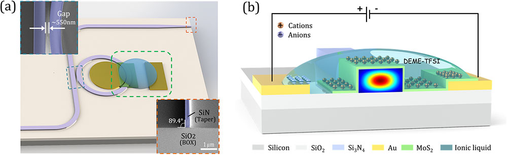
Figure 1.(a) Schematic of a few-layer
As shown in Fig. 2(a), the broadband linear absorption spectrum of few-layer film is measured ranging from 500 nm to 2000 nm. The A and B peaks around visible regime belong to the A and B exciton absorption of and indicate a high quality of film. The linear transmission of film at 1550 nm wave band is measured to be . The small linear absorption contributes to decreasing the insertion loss of film when transferred on the surface of the resonator waveguide. The thickness of used in our experiment is measured to be [Fig. 2(a), inset] by an atomic force microscope (AFM), which indicates the number of layers is about 8 (considering thickness for single layer prepared by mechanical exfoliation method) [36]. The Raman spectrometer is used with 532 nm excitation wavelength to characterize the crystal quality of transferred film, and the results are shown in Fig. 2(b). The two peaks indicate the in-plane vibrational modes of the Mo and S atoms () and the out-of-plane vibrational mode of S atoms (), respectively. The film with high crystal quality contributes to the light–matter interaction more efficiently and further improves the performance of heterostructure integrated photonic devices.
Figure 2.(a) Broadband linear absorption spectrum of few-layer
The bias voltage is applied across the two electrodes to achieve electrostatic doping of the film via ionic liquid (). First, we set the electrode in direct contact with the film as the negative bias voltage, which results in the accumulation of cations at the interface of film. As shown in Fig. 3(a), the MRR has a resonance near 1549.8 nm. When the bias voltages are gradually increased, the resonance wavelength is redshifted with an offset of at 2.6 V, indicating a strong phase shift of the propagating mode in the MRR. Figure 3(b) shows that the resonance shift has a linear relationship with the applied voltage and the tuning efficiency is calculated to be 29.42 pm/V. According to the relationship of , the half-wave-voltage length product is calculated to be 0.69 V·cm, which is comparable to previous reported results [10,16]. Additionally, we also observe the regular intensity modulation in our MRR, which is mainly caused by the change in coupling conditions and the absorption modulation of few-layer and is discussed in detail in the following section. When the inversed bias voltage is applied, indicating the accumulation of anions at the interface of film [Fig. 4(a)], the normalized transmission response of the MRR is also redshifted with a linear relationship for the applied voltages, but the tuning efficiency is calculated to be as low as 10.35 pm/V at [Fig. 4(b)]. Interestingly, as shown in Fig. 5(a), when we continue to increase the bias voltage, the offset of the resonance wavelength loses its linearity at and tends to a similar saturation state. When the applied voltage is further changed from to , the maximum wavelength offset is measured to be relative to the resonance wavelength at [Fig. 5(b)]. The variation of the effective index at different bias voltages is extracted from the normalized transmission spectra [10]. When the interface of is cations doped, the effective index of the composite waveguide changes linearly during the voltage increase. The maximum offset of the effective index reaches at a bias voltage of 3.8 V. When inversed bias voltages are applied, the effective index of the composite waveguide also changes linearly before with a maximum value of . However, the effective index displays a saturable state when the bias voltage is further adjusted with a range from to .
Figure 3.(a) Normalized transmission response of the phase shifter as a function of applied bias voltage (cations doping on the interface of
Figure 4.(a) Normalized transmission response of a phase shifter as a function of applied bias voltage (anion doping on the surface of
Figure 5.(a) Normalized transmission response of a phase shifter at high bias voltages. (b) The offset of resonance wavelength loses its linearity at
Interestingly, besides the phase modulation, the output spectra under different types of charge doping also display regular intensity modulation, which is desired for enormous applications such as optical frequency combs and microwave photonics. Unlike the monolayer that is nearly transparent in the NIR band, few-layer has been demonstrated with a certain absorption capacity at NIR wavelengths [39,40]. Figure 6 shows the relationship between the effective index of the composite waveguide and the applied voltages. The inset images are the energy-band diagram of few-layer under different types of charged doping. Note that few-layer used in our experiment is an n-type semiconductor, which is consistent with previously reported results [41,42]. As shown in Fig. 6, when film is charged-doped by cations under voltages ranging from 0 V to 3.8 V, the effective index of the composite –SiN waveguide increases linearly with the increase of bias voltage, which redshifts the resonant wavelength. At the same time, because the Fermi level of film is adjusted to the conduction band, the absorption of light by the film becomes smaller. Finally, the coupling intensity of the MRR reaches the maximum, and the change of effective index is calculated to be at 1.4 V bias voltage shown in Fig. 3(a). When the bias voltage is further increased, because the absorption of the film has reached the minimum, the further increase of the effective index of the composite waveguide causes the shift of the resonant wavelength and changes the critical coupling to the over-coupling, which leads the coupling intensity to decrease again. In contrast, since the density of states (DOS) in the valence band of is less than that in the conduction band, the accumulated charge of the valence band is also smaller than that of conduction band [43–45]. As shown in Fig. 6, when the interface of film is doped with anions, the effective index of the composite waveguide increases linearly with the increase of bias voltage in the range from 0 V to and redshifts the resonant wavelength. Since the Fermi level adjustment of the film tends to its valence band, the absorption induced from can be enhanced, thereby further introducing larger losses in the micro-ring cavity. The coupling state of the MRR remains at under-coupling. The coupling intensity of the MRR to the incident light is the lowest at the bias voltage ranging from to . However, when the voltage is further increased, the absorption due to the film has reached the maximum value. Meanwhile, the anion doping makes the effective index change of the composite waveguide in the range from to approach saturation with a change amount of about , which is less than the refractive index offset () of the same bias voltage by cation doping. Therefore, within this range, the MRR is always in an under-coupling state. Note that the coupling intensity of the MRR to incident light varies with a small change in the effective index of the composite waveguide.
Figure 6.The effective index of the composite
In Table 1, we compare the performance of the present hybrid integrated device with the state-of-the-art, including silicon–graphene-hybrid MZMs, silicon–-hybrid MZMs, silicon–organic-hybrid MZMs, SiN–PZT-hybrid MRRs, SiN–-hybrid MRRs, and SiN–TMD-hybrid MRRs. Here, we focus on the cross section of waveguide and the phase tuning efficiency of each device, which are key merits to represent the propagation loss and modulation efficiency. As shown in Table 1, our device is the only one to achieve low at a thick SiN platform. In particular, a thick SiN waveguide possesses a lower propagation loss (typical ) than that of a thin SiN waveguide, which requires a cladding layer to reduce the insertion loss. In addition, a thick SiN waveguide enables us to achieve dispersion engineering, which can be used to integrate with other functional devices such as Kerr optical frequency combs and tunable delay lines at a single chip. The demonstrated of our device is also promising, which is only surpassed by the silicon–graphene-hybrid MZMs with a much higher waveguide propagation loss and electrical power consumption. Our proposed device has a simple processing flow, which is more suitable for large-scale photonic systems with low electrical power dissipation and high performance. Moreover, in order to further reduce the insertion loss introduced to the MRRs after transfer, a CMOS-compatible patterning process can be used to precisely pattern the shape of the transferred material and remove excess material. Comparison of Phase Tuning Efficiency for the Hybrid Integrated Phase Modulator MZM, Mach–Zehnder modulator; PZT, piezoelectric lead zirconate titanate; Racetrack, racetrack resonator.Platform Structure Method Cross Section of Waveguide Insertion Loss (dB) Refs. SOI MZM Graphene–silicon / 0.28 [ SOI MZM 2.5 2.2 [ SOI MZM Organic–silicon 5.4 1.4 [ SOI MZM ITO–silicon 6.7 0.0095 [ SiN MRR PZT–SiN / 3.3 [ SiN Racetrack 13 5.1 [ SiN MZM 1.7 [ MRR / 0.8 SiN MRR 3.2 0.69 This work
3. CONCLUSION
We have experimentally demonstrated a heterostructure integrated MRR phase shifter with electrostatically doping ionic liquid. The chemically assisted wet transfer method is used to uniformly clad few-layer on the surface of the SiN waveguide. The effective index of the composite waveguide is studied via adjusting bias voltages to achieve different charged doping induced electro-refractive responses in film. The experimental results demonstrate that our phase shifter has a phase tuning efficiency reaching 29.42 pm/V and is calculated to be 0.69 V·cm. The maximum change in the effective index with cation doping film is measured to be at 3.8 V. Additionally, when applying the anion doping to the interface of film, the maximum change in the effective index of composite is about at bias voltage, and the saturation phenomenon is also observed. Since the resonator is designed near the critical coupling regime, during the charged doping process, the coupling condition between the bus waveguide and MRR can be engineered from under-coupling to over-coupling. That can be involved as a degree of freedom for the coupling tailoring. The proposed phase shifter presents a facile scheme to be hybrid with 2DLMs and to be realized on a thick SiN platform, which is promising for compact MRR structures and might be used as a promising phase modulation scheme for large-scale optical links with ultralow loss and power consumption.
References
[1] S. Brian, X. C. Ji, Y. Okawachi, A. L. Gaeta, M. Lipson. Battery-operated integrated frequency comb generator. Nature, 562, 401-405(2018).
[2] M. La Notte, B. Troia, T. Muciaccia, C. E. Campanella, F. De Leonardis, V. M. N. Passaro. Recent advances in gas and chemical detection by Vernier effect-based photonic sensors. Sensors, 14, 4831-4855(2014).
[3] Y. Tao, H. Shu, X. Wang, M. Jin, Z. Tao, F. Yang, J. Shi, J. Qin. Hybrid-integrated high-performance microwave photonic filter with switchable response. Photon. Res., 9, 1569-1580(2021).
[4] X. Xue, X. Zheng, B. Zhou. Super-efficient temporal solitons in mutually coupled optical cavities. Nat. Photonics, 13, 616-622(2019).
[5] Y. Okawachi, M. Lamont, K. Luke, D. Carvalho, M. Yu, M. Lipson, A. L. Gaeta. Bandwidth shaping of microresonator-based frequency combs via dispersion engineering. Opt. Lett., 39, 3535-3538(2014).
[6] Y. Zhao, X. Ji, B. Y. Kim, P. S. Donvalkar, J. K. Jang, C. Joshi, M. Yu, C. Joshi, R. R. Domeneguetti, F. A. S. Barbosa, P. Nussenzveig, Y. Okawachi, M. Lipson, A. L. Gaeta. Visible nonlinear photonics via high-order-mode dispersion engineering. Optica, 7, 135-141(2020).
[7] S. Yang, D. C. Liu, Z. L. Tan, K. Liu, Z. H. Zhu, S. Q. Qin. CMOS-compatible WS2-based all-optical modulator. ACS Photon., 5, 342-346(2018).
[8] H. Lin, Z. Luo, T. Gu, L. C. Kimerling, K. Wada, A. Agarwal, J. Hu. Mid-infrared integrated photonics on silicon: a perspective. Nanophotonics, 7, 393-420(2018).
[9] V. Sorianello, M. Midrio, G. Contestabile, I. Asselberghs, J. Van Campenhout, C. Huyghebaert, I. Goykhman, A. K. Ott, A. C. Ferrari, M. Romagnoli. Graphene–silicon phase modulators with gigahertz bandwidth. Nat. Photonics, 12, 40-44(2018).
[10] I. Datta, S. H. Chae, G. R. Bhatt, M. A. Tadayon, B. Li, Y. Yu, C. Park, J. Park, L. Cao, D. N. Basov, J. Hone, M. Lipson. Low-loss composite photonic platform based on 2D semiconductor monolayers. Nat. Photonics, 14, 256-262(2020).
[11] R. Zhang, J. A. Ma. Simple bidirectional hybrid optical link for alternatively providing wired and wireless accesses based on an optical phase modulator. Photon. Netw. Commun., 34, 478-485(2017).
[12] W. Zhang, M. Ebert, B. Chen, J. D. Reynolds, X. Yan, H. Du, M. Banakar, D. T. Tran, K. Debnath, C. G. Littlejohns, S. Saito, D. J. Thomson. Integration of low loss vertical slot waveguides on SOI photonic platforms for high efficiency carrier accumulation modulators. Opt. Express, 28, 23143-23153(2020).
[13] F. Eltes, G. E. Villarreal-Garcia, D. Caimi, H. Siegwart, A. A. Gentile, A. Hart, P. Stark, G. D. Marshall, M. G. Thompson, J. Barreto, J. Fompeyrine, S. Abel. An integrated optical modulator operating at cryogenic temperatures. Nat. Mater., 19, 1164-1168(2020).
[14] J. E. Ortmann, F. Eltes, D. Caimi, N. Meier, A. A. Demkov, L. Czornomaz, J. Fompeyrine, S. Abel. Ultra-low-power tuning in hybrid barium titanate–silicon nitride electro-optic devices on silicon. ACS Photon., 6, 2677-2684(2019).
[15] N. Ahmed, S. Shi, A. J. Mercante, D. W. Prather. High-performance racetrack resonator in silicon nitride thin film lithium niobate hybrid platform. Opt. Express, 27, 30741-30751(2019).
[16] K. Alexander, J. P. George, J. Verbist, K. Neyts, B. Kuyken, D. V. Thourhout, J. Beeckman. Nanophotonic Pockels modulators on a silicon nitride platform. Nat. Commun., 9, 3444(2018).
[17] P. Zhang, H. Huang, Y. Jiang, X. Han, H. Xiao, A. Frigg, T. G. Nguyen, A. Boes, G. Ren, Y. Su, Y. Tian, A. Mitchell. High-speed electro-optic modulator based on silicon nitride loaded lithium niobate on an insulator platform. Opt. Lett., 46, 5986-5989(2021).
[18] C. Phare, Y. H. Daniel Lee, J. Cardenas, M. Lipson. Graphene electro-optic modulator with 30 GHz bandwidth. Nat. Photonics, 9, 511-514(2015).
[19] J. Wang, X. Zhang, Y. Chen, Y. Geng, Y. Du, X. Li. Design of a graphene-based silicon nitride multimode waveguide-integrated electro-optic modulator. Opt. Commun., 481, 126531(2021).
[20] C. Qiu, Y. Yang, C. Li, Y. Wang, K. Wu, J. Chen. All-optical control of light on a graphene-on-silicon nitride chip using thermo-optic effect. Sci. Rep., 7, 17046(2017).
[21] Z. Ruan, L. Pei, J. Wang, J. Zheng, J. Wang, J. Li, T. Ning, Q. Zhao, Y. Xi. All-optical graphene oxide modulator based on phase-shifted FBG. J. Lightwave Technol., 39, 5516-5522(2021).
[22] Y. Meng, S. Ye, Y. Shen, Q. Xiao, X. Fu, R. Lu, Y. Liu, M. Gong. Waveguide engineering of graphene optoelectronics—modulators and polarizers. IEEE Photon. J., 10, 6600217(2018).
[23] K. F. Mak, C. Lee, J. Hone, J. Shan, T. F. Heinz. Atomically thin MoS2: a new direct-gap semiconductor. Phys. Rev. Lett., 105, 136805(2010).
[24] T. Chu, H. Ilatikhameneh, G. Klimeck, R. Rahman, Z. Chen. Electrically tunable bandgaps in bilayer MoS2. Nano Lett., 15, 8000-8007(2015).
[25] K. Mak, K. He, C. Lee, J. Hone, T. F. Heinz, J. Shan. Tightly bound trions in monolayer MoS2. Nat. Mater., 12, 207-211(2013).
[26] N. Peimyoo, T. Deilmann, F. Withers, J. Escolar, D. Nutting, T. Taniguchi, K. Watanabe, A. Taghizadeh, M. F. Craciun, K. S. Thygesen, S. Russo. Electrical tuning of optically active interlayer excitons in bilayer MoS2. Nat. Nanotechnol., 16, 888-893(2021).
[27] W. Zhao, S. Bi, C. Zhang, P. D. Rack, G. Feng. Adding solvent into ionic liquid-gated transistor: the anatomy of enhanced gating performance. ACS Appl. Mater. Interfaces, 11, 13822-13830(2019).
[28] Y. Zhang, J. Ye, Y. Matsuhashi, Y. Iwasa. Ambipolar MoS2 thin flake transistors. Nano Lett., 12, 1136-1140(2012).
[29] T. H. Tsai, A. K. Sahoo, H. K. Syu, Y. C. Wu, M. Y. Tsai, M. D. Siao, Y. C. Yang, Y. F. Lin, R. S. Liu, P. W. Chiu. WS2/WSe2 nanodot composite photodetectors for fast and sensitive light detection. ACS Appl. Electron. Mater., 3, 4291-4299(2021).
[30] Y. Sun, R. Hu, C. An, X. Ma, J. Zhang, J. Liu. Visible to near-infrared photodetector based on SnSe2/WSe2 heterojunction with potential application in artificial visual neuron. Nanotechnology, 32, 475206(2021).
[31] G. Wei, T. K. Stanev, D. A. Czaplewski, I. W. Jung, N. P. Stern. Silicon-nitride photonic circuits interfaced with monolayer MoS2. Appl. Phys. Lett., 107, 091112(2015).
[32] Y. Dai, Y. Wang, S. Das, H. Xue, X. Bai, E. Hulkko, Z. Sun. Electrical control of interband resonant nonlinear optics in monolayer MoS2. ACS Nano, 14, 8442-8448(2020).
[33] E. J. G. Santos, E. Kaxiras. Electrically driven tuning of the dielectric constant in MoS2 layers. ACS Nano, 7, 10741-10746(2013).
[34] S. Wang, H. Yu, H. Zhang, A. Wang, M. Zhao, Y. Chen, L. Mei, J. Wang. Broadband few-layer MoS2 saturable absorbers. Adv. Mater., 26, 3538-3544(2014).
[35] Y. Zhou, L. Tao, Z. Chen, H. Lai, W. Xie, J. Xu. Defect etching of phase-transition-assisted CVD-grown 2H-MoTe2. Small, 17, 2102146(2021).
[36] B. Radisavljevic, A. Radenovic, J. Brivio, V. Giacometti, A. Kis. Single-layer MoS2 transistors. Nat. Nanotechnol., 6, 147-150(2011).
[37] Y. Rho, J. Pei, L. Wang, Z. Su, M. Eliceiri, C. P. Grigoropoulos. Site-selective atomic layer precision thinning of MoS2 via laser-assisted anisotropic chemical etching. ACS Appl. Mater. Interfaces, 11, 39385-39393(2019).
[38] X. Ji, F. Barbosa, S. P. Roberts, A. Dutt, J. Cardenas, Y. Okawachi, A. Bryant, A. L. Gaeta, M. Lipson. Ultra-low-loss on-chip resonators with sub-milliwatt parametric oscillation threshold. Optica, 4, 619-624(2017).
[39] M. Zhang, R. C. Howe, R. I. Woodward, E. J. Kelleher, F. Torrisi, G. Hu, T. Hasan. Solution processed MoS2-PVA composite for sub-bandgap mode-locking of a wideband tunable ultrafast Er:fiber laser. Nano Res., 8, 1522-1534(2015).
[40] K. Wu, X. Zhang, J. Wang, J. Chen. 463-MHz fundamental mode-locked fiber laser based on few-layer MoS2 saturable absorber. Opt. Lett., 40, 1374-1377(2015).
[41] A. Pezeshki, S. H. H. Shokouh, T. Nazari, K. Oh, S. Im. Electric and photovoltaic behavior of a few-layer α-MoTe2/MoS2 dichalcogenide heterojunction. Adv. Mater., 28, 3216-3222(2016).
[42] S. Rathi, I. Lee, D. Lim, J. Wang, Y. Ochiai, N. Aoki, K. Watanabe, T. Taniguchi, G.-H. Lee, Y.-J. Yu, P. Kim, G.-H. Kim. Tunable electrical and optical characteristics in monolayer graphene and few-layer MoS2 heterostructure devices. Nano Lett., 15, 5017-5024(2015).
[43] D. Braga, I. G. Lezama, H. Berger, A. F. Morpurgo. Quantitative determination of the band gap of WS2 with ambipolar ionic liquid-gated transistors. Nano Lett., 12, 5218-5223(2012).
[44] A. Kuc, N. Zibouche, T. Heine. Influence of quantum confinement on the electronic structure of the transition metal sulfide TS2. Phys. Rev. B., 83, 245213(2011).
[45] Y. Ding, X. Zhu, S. Xiao, H. Hu, L. H. Frandsen, N. A. Mortensen, K. Yvind. Effective electro-optical modulation with high extinction ratio by a graphene–silicon microring resonator. Nano Lett., 15, 4393-4400(2015).
[46] M. He, M. Xu, Y. Ren, J. Jian, Z. Ruan, Y. Xu, S. Gao, S. Sun, X. Wen, L. Zhou, L. Liu, C. Guo, H. Chen, S. Yu, L. Liu, X. Cai. High-performance hybrid silicon and lithium niobate Mach–Zehnder modulators for 100 Gbit s−1 and beyond. Nat. Photonics, 13, 359-364(2019).
[47] M. Li, L. Wang, X. Li, X. Xiao, S. Yu. Silicon intensity Mach–Zehnder modulator for single lane 100 Gb/s applications. Photon. Res., 6, 109-116(2018).
[48] R. Amin, R. Maiti, Y. Gui, C. Suer, M. Miscuglio, E. Heidari, R. T. Chen, H. Dalir, V. J. Sorger. Sub-wavelength GHz-fast broadband ITO Mach–Zehnder modulator on silicon photonics. Optica, 7, 333-335(2020).
[49] W. Jin, R. G. Polcawich, P. A. Morton, J. E. Bowers. Piezoelectrically tuned silicon nitride ring resonator. Opt. Express, 26, 3174-3187(2018).
Set citation alerts for the article
Please enter your email address