• Photonics Research
  • Vol. 10, Issue 6, 1440 (2022)
Guohui Li1, Huihui Pi1, Yanfu Wei1, Bolin Zhou1, Ya Gao1, Rong Wen1, Yuying Hao1, Han Zhang2、4, Beng S. Ong3、5, and Yanxia Cui1、*
Author Affiliations
  • 1College of Physics and Optoelectronics, Key Laboratory of Interface Science and Engineering in Advanced Materials, Key Laboratory of Advanced Transducers and Intelligent Control System of Ministry of Education, Taiyuan University of Technology, Taiyuan 030024, China
  • 2Collaborative Innovation Centre for Optoelectronic Science and Technology, Key Laboratory of Optoelectronic Devices and Systems of Ministry of Education and Guangdong Province, College of Physics and Optoelectronic Engineering, Shenzhen Key Laboratory of Micro-Nano Photonic Information Technology, Guangdong Laboratory of Artificial Intelligence and Digital Economy (SZ), Shenzhen University, Shenzhen 518060, China
  • 3Department of Chemistry, Research Centre of Excellence for Organic Electronics, Institute of Advanced Materials, Hong Kong Baptist University, Kowloon Tong, Hong Kong, China
  • 4e-mail: hzhang@szu.edu.cn
  • 5e-mail: bong@hkbu.edu.hk
  • show less
    DOI: 10.1364/PRJ.452620 Cite this Article Set citation alerts
    Guohui Li, Huihui Pi, Yanfu Wei, Bolin Zhou, Ya Gao, Rong Wen, Yuying Hao, Han Zhang, Beng S. Ong, Yanxia Cui. Passivation of degradation path enables high performance perovskite nanoplatelet lasers with high operational stability[J]. Photonics Research, 2022, 10(6): 1440 Copy Citation Text show less

    Abstract

    MAPbI3 perovskite has attracted widespread interests for developing low-cost near infrared semiconductor gain media. However, it faces the instability issue under operation conditions, which remains a critical challenge. It is found that the instability of the MAPbI3 nanoplatelet laser comes from the thermal-induced degradation progressing from the surface defects towards neighboring regions. By using PbI2 passivation, the defect-initiated degradation is significantly suppressed and the nanoplatelet degrades in a layer-by-layer way, enabling the MAPbI3 laser to sustain for 4500 s (2.7×10⁷ pulses), which is nearly three times longer than that of the nanoplatelet laser without passivation. Meanwhile, the PbI2 passivated MAPbI3 nanoplatelet laser with the nanoplatelet cavity displays a maximum quality factor up to 7800, the highest reported for all MAPbI3 nanoplatelet cavities. Furthermore, a high stability MAPbI3 nanoplatelet laser that can last for 8500 s (5.1×10⁷ pulses) is demonstrated based on a dual passivation strategy, by retarding the defect-initiated degradation and surface-initiated degradation simultaneously. This work provides in-depth insights for understanding the operating degradation of perovskite lasers, and the dual passivation strategy paves the way for developing high stability near infrared semiconductor laser media.

    1. INTRODUCTION

    Near infrared semiconductor nanolasers are of great significance for integrated optoelectronic chips [13]. An efficient gain medium is one of the key components of near infrared nanolasers [46]. The traditional gain media of near infrared lasers are made of inorganic semiconductors, but their quantum efficiencies are low and the growths require critical conditions [3]. Perovskites have attracted considerable interests and have been considered as leading-candidate gain media for next generation on-chip optical sources, thanks to their outstanding photophysical properties as well as low cost and promise for electrically driven lasing [710]. Among various perovskite materials, organic–inorganic hybrid materials, with MAPbI3 as a representative, are of particular interest in the fields of semiconductor lasers as well as solar cells [11,12], light emitting diodes [13], photodetectors [14], etc., due to their large absorption coefficients, exceptionally low trap-state densities, large charge carrier diffusion lengths, and high charge mobilities [15].

    In recent years, organic–inorganic hybrid perovskite lasers have achieved rapid progress. Zhang et al. achieved a room-temperature MAPbI3 nanoplatelet laser with a lasing threshold of 37  μJcm2 and a cavity quality factor of 650 through the vapor phase deposition method [3]. Zhu et al. demonstrated room-temperature lasing using solution-processed single-crystalline MAPbI3 nanowires, which showed a lasing threshold down to 220  nJcm2 and a cavity quality factor Q as high as 3600 [1]. Jia et al. demonstrated continuous wave lasing by an MAPbI3 distributed feedback laser at a substrate temperature of 102 K [16]. In 2020, Qin et al. achieved continuous wave pumped lasing with quasi-2D phenylethylammonium bromide and 1-naphthylmethylamibe bromide based perovskite media in air at room temperature [17]. Although various inorganic cations have been proposed to replace the organic cation [1820] and different lead-free perovskite materials have also been developed [2123], their lasing characteristics including the lasing threshold and cavity quality factor performed well below those of the organic–inorganic Pb based counterparts up to now [11].

    However, organic and inorganic hybrid perovskites suffer from instability under operating conditions. It was reported that the temperature of a distributed feedback MAPbI3 laser on sapphire increased by 30 K after pumping for 50 ns and then by 90 K for 1 ms [24]. Such a temperature increase can result in thermal-induced degradation of perovskite crystals. Fan et al. found that the crystalline structure gradually evolved from tetragonal MAPbI3 to trigonal layered PbI2 after the temperature increased to 358 K [25]. Ascribed to the detrimental temperature increase, most of the organic and inorganic hybrid perovskite lasers could not sustain more than 107  pulses. For example, the emission intensity of an inkjet-printed MAPbI3 laser on a flexible PET substrate with a nanoimprinted grating in N2 atmosphere dropped to 90% of its initial value after 1×10⁶  pulses [26]. The MAPbI3 laser with a silica microsphere resonator could sustain by 8.6×10⁶  pulses [2]. Similarly, solution-processed FAPbBr3 microdisk lasers could work stably for 3000 s (3×10⁶  pulses) before dropping to 90% of the initial value [27].

    On the one hand, promoting the operating stability of lasers is one of the constant tasks of laser technology [28]. Although room-temperature continuous wave perovskite lasers have been reported [17], one of the major hurdles towards electrically pumped lasers is resistive heating under current injection [7]. On the other hand, improving the thermal stability is of critical importance for achieving electrically pumped perovskite lasers. Until now, great efforts have been made to improve the stability of organic–inorganic perovskites while maintaining their outstanding photophysical properties [2931]. Working at cryogenic temperatures to keep perovskites below thermal degradation temperature is helpful to promote the stability of perovskite lasers. For example, CW amplified spontaneous emission (ASE) in a phase-stable perovskite has been demonstrated at temperatures up to 120 K [32]. However, room-temperature operating lasers are preferred in most applications [28]. The encapsulation strategy has been resorted to improve the perovskite lasing stability. For example, a thin poly-methyl-methacrylate (PMMA) encapsulation layer was applied in an MAPbI3 photonic crystal laser so that the operational stability at a pump intensity of 102.5±6.4  μJ/cm2 was extended from 600 s (105  pulses) to 6000 s (106  pulses) [33]. By using a CYTOP encapsulation film, an MAPbI3 distributed feedback laser that operated at a pump intensity of 7  μJ/cm2 could sustain 107  pulses before dropping to 90% of its initial value [34]. It was also demonstrated that the stability of MAPbI3 could be improved by encapsulating with boron nitride flakes [25]. Nevertheless, the stability performance of hybrid perovskite lasers is still dissatisfactory. Improving their stability is still one of the major tasks in this field, which is what has been done in the organic display industry [35]. For example, perovskite microlasers with longer lifetime can produce stronger signal and sustain for longer measurement times, which will generate a better signal to noise ratio for sensors [36]. The ultimate goal is to achieve perovskite laser diodes with lifetimes of many thousands of hours that are capable of supporting many commercial applications [7,37].

    Understanding the degradation mechanisms is of significant importance for improving the operating stability of perovskite lasers. MAPbI3 perovskite is reported to evolve from tetragonal MAPbI3 to trigonal lead iodide layered crystal layer by layer due to the fact that a surface-initiated layer by layer degradation path exhibits the lowest energy barrier for crystal transition under moderate heating at 358 K in 2017 [25]. With the rapid development of the perovskite solar cell, the degradation mechanisms of operating perovskite solar cells have received widespread interest in recent years. The degradation behavior of perovskite solar cells was found to be profoundly influenced by macroscopic operation conditions in 2018 [38]. In perovskite solar cells, the performance degradation after hundreds of hours of operation in N2 atmosphere was found to be induced by cation-dependent phase segregation during device operation in 2020 [39]. Degradation of operating perovskite solar cells under vacuum was considered to be caused by a large degree of lattice shrinkage and a spontaneous process for phase segregation in 2021 [40]. Compared with standard one sun illumination (1.5  kW/m2) in PSC, perovskite lasers are illuminated by much stronger laser light (peak intensity up to 650  GW/m2) and degrade after outputting 107  pulses. Pumped by a femtosecond laser with a repetition rate of 250 kHz, perovskite lasers will degrade after tens of minutes, which is much shorter than that of PSCs. Therefore, the faster degradation process of perovskite lasers cannot be explained by lattice shrinkage and phase segregation, which are responsible for the degradation of PSCs. To direct scientific progress towards more applications, the microscopic degradation mechanism for hybrid perovskite during the laser pumping process needs to be fully understood.

    In this work, by continuously monitoring the emission properties of an MAPbI3 nanoplatelet laser, we find that the gradual degradation of tetragonal MAPbI3 starts from the surface defects and the laser output intensity drops to 90% after 1200  s (7.2×10⁶  pulses). Those surface defects on the MAPbI3 nanoplatelets can be effectively passivated by introducing excess PbI2. As a result, the evolution from tetragonal MAPbI3 to PbI2 launches from the crystal surface and the nanoplatelet degrades layer by layer, bringing forward the operational stability being extended from 1200 s to 4500 s (2.7×10⁷  pulses). On the basis of the PbI2 passivated nanoplatelet, we further introduce an additional DBP (C64H36) protection film, which can suppress the surface-initiated degradation by passivating the surface dangling bonds, thereby dramatically improving the operational stability of the MAPbI3 laser to up to 8500 s (5.1×10⁷  pulses), which is around 1.89 times as long as that of the MAPbI3 nanoplatelet with only PbI2 passivation. Compared with the initial MAPbI3 nanoplatelets with surface defects, the dual passivation strategy with both PbI2 and DBP enables the MAPbI3 laser to sustain for six times longer, promoting the stability performance of MAPbI3 perovskite lasers significantly. The present passivation strategy of improving the perovskite laser stability paves the way for developing high stability near infrared gain media. In addition, our first attempt at demonstrating the degradation mechanism of the hybrid perovskite crystals under laser pumping might provide in-depth insights for resolving the critical stability hurdle in practical applications of perovskite lasers.

    2. RESULTS AND DISCUSSION

    The MAPbI3 nanoplatelets used in our study were synthesized by the two-step chemical vapor deposition method (see Appendix A for more details), which includes a first step of growing PbI2 nanoplatelets and a second step of converting PbI2 nanoplatelets into MAPbI3 nanoplatelets. The lasing threshold of an unpassivated nanoplatelet laser can be as low as 18.0  μJ/cm2 (see Appendix B). We measured the time-resolved photoluminescence (TRPL) of an MAPbI3 nanoplatelet laser without passivation (see Appendix B). Since MAPbI3 crystals show both fast dynamics and slow dynamics, biexponential fitting was performed to quantify the carrier dynamics. Here, the slow decay component reveals the lifetime of carriers [41]. At a pump intensity of 17.87  μJ/cm2 (below threshold), the PL decay curve shows a long average lifetime of 1.74  ns. At a pump intensity of 26.81  μJ/cm2 (above the threshold), the PL decay curve shows a short average lifetime of 0.86  ns. More information of MAPbI3 nanoplatelet lasers without passivation can be found in our previous work [42]. As MAPbI3 perovskite is very sensitive to electron-beam irradiation and begins to decompose into PbI2 under 151  e2 total dose irradiation [43], monitoring the degradation process continuously with scanning electron microscopy (SEM) will introduce radiation damage. Therefore, only one SEM measurement is made on a nanoplatelet and the time is controlled within 1 min to avoid total dose irradiation exceeding 151  e2. We continuously monitored the emission properties and the spectra of the MAPbI3 nanoplatelet laser in ambient air conditions with a home-built microscopic imaging and excitation system (see Appendix A for more details) in the operational stability measurement.

    The degradation evolution of an MAPbI3 nanoplatelet laser operating at a pumping intensity of 26.1  μJ/cm2 (1.1Pth) is shown in Fig. 1(a). In order to illustrate the degradation process better, the degradation region is marked with dashed lines. As can be seen in microscopic images, the emission intensity was almost uniform during the first 300 s. After operating for 500 s, the emission intensity on the left side of the laser started to decrease, which indicates that parts of the MAPbI3 molecules degrade to molecules that do not emit light in the monitoring spectral region. After operating for 700 s, the dark area expands to neighboring regions, which is different from the layer-to-layer degradation demonstrated in a previous report [25]. After operating for 900 s, the dark area continues to expand to neighboring regions. After operating for 1100 s, the dark area expands to the edge of the nanoplatelet. Therefore, we can conclude that the degradation propagated to the surrounding areas during the operating process. Since the measurement takes a long time, the emission intensity of the laser operating at a pump intensity of 1.1Pth (26.1  μJ/cm2) during the operating time was measured using an ideaoptics PG2000-Pro spectrometer (see Appendix A for more details) as shown in Fig. 1(b). As can be seen, the laser output intensity as a whole does not change, because more pumping energy can reach a lower MAPbI3 layer, which keeps the population inversion ΔN required for maintaining the output intensity IΔN almost unchanged as the upper layer of MAPbI3 degrades (see Appendix C for more details). After operating for 1200 s (7.2×10⁶  pulses), the output intensity of the nanoplatelet laser decreases to 90% of the initial intensity as can be seen in Fig. 1(b). The operational stability data are in agreement with most of the reported MAPbI3 lasers [1,34]. After operating for 1100 s, the dark area keeps increasing and the output intensity of the nanoplatelet laser decreases dramatically. The laser dies after working for 1750 s. Besides this nanoplatelet laser, the operational stability of two other unpassivated nanoplatelet lasers has also been measured. The two nanoplatelet lasers can sustain for 1170 s and 1200 s (see Appendix B) before the output intensity decreases to 90% of its initial values, which are consistent with that of the first nanoplatelet laser.

    (a) Microscopic image of an MAPbI3 laser operating at a pump intensity of 1.1Pth (26.1 μJ/cm2) after working for different times. (b) Lasing stability data of MAPbI3 laser under femtosecond laser pumping with a repetition rate of 6 kHz in ambient air condition. (c) Spectrum evolution of MAPbI3 laser operating at a pump intensity of 1.1Pth (26.1 μJ/cm2) after working for different times. (d) Microscopic image of the nanoplatelet after operating for 1800 s. (e) Microscopic image and SEM image of the initial MAPbI3 nanoplatelet with surface defects. (f) Atomic force microscopic image of the MAPbI3 nanoplatelet shows that its RMS roughness is 2.1 nm.

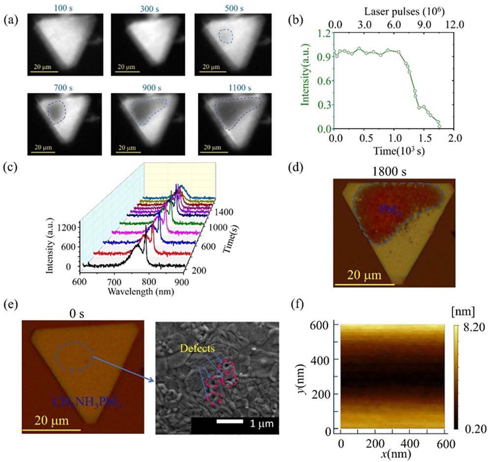
    Figure 1.(a) Microscopic image of an MAPbI3 laser operating at a pump intensity of 1.1Pth (26.1  μJ/cm2) after working for different times. (b) Lasing stability data of MAPbI3 laser under femtosecond laser pumping with a repetition rate of 6 kHz in ambient air condition. (c) Spectrum evolution of MAPbI3 laser operating at a pump intensity of 1.1Pth (26.1  μJ/cm2) after working for different times. (d) Microscopic image of the nanoplatelet after operating for 1800 s. (e) Microscopic image and SEM image of the initial MAPbI3 nanoplatelet with surface defects. (f) Atomic force microscopic image of the MAPbI3 nanoplatelet shows that its RMS roughness is 2.1 nm.

    The emission spectrum evolutions of the laser operating at a pump intensity of 1.1Pth (26.1  μJ/cm2) during the operating time were also measured by using an ideaoptics PG2000-Pro spectrometer (see Appendix A for more details). From the emission spectrum as shown in Fig. 1(c), we can see that the intensity of the laser line after operating for 1000 s starts to decrease with the decreasing spontaneous emission intensity. After 1800 s, the spontaneous emission intensity drops down to 50% of its initial value and the laser line almost disappears at the same time (see Appendix B). As can be seen in the microscopic image [Fig. 1(d)] of the MAPbI3 nanoplatelet after operating for 1800 s, part of the nanoplatelet marked with a dashed line has faster degradations, and the color of this part has changed to brown as compared with the yellow color of the other regions, which is similar to the initial color of the MAPbI3 nanoplatelet as shown in Fig. 1(e).

    From the microscopic image of the initial MAPbI3 nanoplatelet as shown in Fig. 1(e), it is seen that the nanoplatelet with a thickness of 130  nm (see Appendix B) initially has a uniform surface and the whole surface is almost the same yellow color. However, from the SEM image of the MAPbI3 nanoplatelets, some surface defects are found on the surface, as can be seen in Fig. 1(e). Defects are mainly located at perovskite grain boundaries, which is in good agreement with previous results [44]. Atomic force microscopy (AFM) image [Fig. 1(f)] of the nanoplatelets shows that the RMS roughness of the surface is 2.1  nm. As can be seen in Fig. 1(f), there is a trench that almost covers the whole image in the 600  nm×600  nm region. Its depth is 8  nm. Therefore, the MAPbI3 nanoplatelet under operating condition starts to degrade from surface defects and progresses gradually to neighboring areas as shown in Fig. 1(a). The corresponding X-ray diffraction (XRD) pattern shows that the perovskite nanoplatelets initially have a pure tetragonal MAPbI3 crystal structure without impurities such as PbI2 (see Appendix B). The existence of the small (202), (112), (210), and (221) peaks indicates that the MAPbI3 nanoplatelets are in the room-temperature tetragonal phase [45]. After operating for 1800 s, more than a half of the surface has changed from yellow to brown as can be seen in Fig. 1(d). The corresponding XRD pattern shows that (001), (003), and (004) peaks of PbI2 appear after the nanoplatelets operate for 1800 s, confirming that some part of the tetragonal phase MAPbI3 nanoplatelet degrades to PbI2 [45].

    The observed phenomenon of MAPbI3 degradation launching from the surface defects deviates from the layer-by-layer degradation theory, which expresses that the thermal-induced degradation starts from the surface of MAPbI3 as a result of dangling bonds, structure relaxation, and charge redistribution on the surface and occurs in a sequential layer-by-layer style [25]. A calculation of the transient thermal response of an MAPbI3 nanoplatelet shows that, with a moderate laser pump intensity of 17  μJ/cm2, the transient temperature at the nanoplatelet (see Appendix D) far exceeds the thermal degradation threshold temperature [25]. It is unquestionable that the MAPbI3 nanoplatelet suffers detrimental thermal-induced degradation in the experiment. In reality, with respect to the smooth flat surface, the surface defect regions on the surface of the nanoplatelet can form extra dangling bonds on their walls, which initiate new degradation pathways. Since the longer Pb–I–Pb bonds along the [001] direction of MAPbI3 are less resistant to bond breakage than those in the (001) plane [46], these bonds tend to break first under an external stimulus and form dangling bonds. The more defects there are on the nanoplatelet, the faster the speed of the thermal-induced degradation. Under laser operating conditions, the expansion of the defect region would accelerate the degradation, so a snowball effect is produced. Therefore, ascribed to the existence of surface defects, the degradation proceeds from the inner part to the edge rather than following the layer-by-layer degradation theory. It is plausible to suppose that reducing the defects can suppress the degradation and make the nanoplatelet lasers operate for longer times.

    In contrast to fully converting PbI2 to MAPbI3 during the second step of chemical vapor deposition, a certain amount of PbI2 was intentionally reserved to passivate the defects in the fabrication of new perovskite nanoplatelets. As shown in Fig. 2(a), MAPbI3 nanoplatelets with well-defined triangular and hexagonal shape, 100–200 nm thickness, and tens of micrometers edge lengths were synthesized. As can be seen in the XRD pattern [Fig. 2(b)], there also exist (001), (003), and (004) peaks of the PbI2 structure in addition to the tetragonal phase MAPbI3 peaks, confirming the excess PbI2 being reserved in the perovskite nanoplatelets. Figure 2(c) shows the microscopic image of the MAPbI3 nanoplatelet for carrying out the following lasing operation. The perovskite nanoplatelet has a thickness of 180  nm (see Appendix E). The SEM image in Fig. 2(d) reflects that the surface defects were successfully passivated to a large extent. As can be seen, a newly formed species appeared on the nanoplatelet surface, and the new species displayed brighter color as compared with neighboring species as a result of poorer conductivity [47]. According to the XRD pattern as shown in Fig. 2(b), the species should be PbI2, while the darker films are considered to be perovskite. Because the formation energies of defects are generally related to the chemical potentials of the perovskite constituent element, defects can be controlled by adjusting the ratio of I/Pb in perovskite films [47]. It has been reported that the trap density can be reduced through a moderate excess PbI2 passivation [44]. During the chemical vapor deposition process, PbI2 is squeezed to grain boundaries by perovskite grain growth. Thus, the rich defect regions can be passivated by PbI2 and defects can be reduced [Fig. 2(d)]. From the SEM images, it can be clearly observed that the excess PbI2 was mainly distributed on the perovskite grain boundaries. Benefiting from reduced defects, the PbI2 passivated perovskite nanoplatelets have smoother surfaces. The AFM image in Fig. 2(e) indicates an RMS roughness of 0.7  nm, confirming that the nanoplatelets have much smoother surfaces supporting the whispering-gallery-mode cavity after passivation. After PbI2 passivation, there are only two tiny pinholes with diameter of 100  nm and depth of less than 3 nm in a 600  nm×600  nm region as shown in Fig. 2(e).

    (a) Microscopic image of MAPbI3 nanoplatelets on a mica substrate. (b) XRD pattern of the MAPbI3 nanoplatelets. (c) Microscopic image of an MAPbI3 nanoplatelet used for demonstrating the laser before exposure to a pump laser. (d) SEM image of MAPbI3 nanoplatelet. (e) AFM image of MAPbI3 nanoplatelet shows its RMS roughness is ∼0.7 nm. (f) Laser output intensity as a function of pump intensity. (g) Evolution of emission spectra obtained at different pump intensities. (h) Lorentz fitting of a lasing oscillation mode at ≈781.3 nm gives an FWHM of 0.10 nm, corresponding to a Q factor of 7813. (i) Time-resolved photoluminescence (TRPL) spectra of perovskite nanoplatelet operating at spontaneous emission (P=11.12 μJ/cm2) and laser emission condition (P=24.8 μJ/cm2).

    Figure 2.(a) Microscopic image of MAPbI3 nanoplatelets on a mica substrate. (b) XRD pattern of the MAPbI3 nanoplatelets. (c) Microscopic image of an MAPbI3 nanoplatelet used for demonstrating the laser before exposure to a pump laser. (d) SEM image of MAPbI3 nanoplatelet. (e) AFM image of MAPbI3 nanoplatelet shows its RMS roughness is 0.7  nm. (f) Laser output intensity as a function of pump intensity. (g) Evolution of emission spectra obtained at different pump intensities. (h) Lorentz fitting of a lasing oscillation mode at 781.3  nm gives an FWHM of 0.10 nm, corresponding to a Q factor of 7813. (i) Time-resolved photoluminescence (TRPL) spectra of perovskite nanoplatelet operating at spontaneous emission (P=11.12  μJ/cm2) and laser emission condition (P=24.8  μJ/cm2).

    The influence of excess PbI2 on the laser performance is investigated in the following. The light-in–light-out curve in Fig. 2(f) shows that the emission intensity grows slowly with the increasing pump intensity below the pump intensity of 14.98  μJ/cm2, and then the emission intensity grows very quickly. At a pump intensity of 15.87  μJ/cm2, the emission intensity saturates due to blue shift of the center wavelength of the laser [1]. Lasing death did not happen in the measurement. Here, the lasing threshold of 14.98  μJ/cm2 is lower than that of the MAPbI3 nanoplatelet laser without passivation, which can be found in our previous work [42]. Since the spectrum has a narrow linewidth that cannot be resolved by an ideaoptics PG2000-Pro spectrometer, the emission spectrum evolution of the laser operating at different pump intensities was measured by using a Horiba iHR 550 spectrometer (see Appendix A for more information). The spectra of the emission light in Fig. 2(g) show that there exists only spontaneous emission below 14.98  μJ/cm2. Above the threshold, a narrow laser peak appears, and the laser peak increases rapidly with the increasing pump intensity. As shown in Fig. 2(h), the separation between adjacent modes is 0.3  nm, which is in agreement with the theoretical value (0.3  nm) calculated with the edge length of the cavity [42]. A Lorentz fit of the laser peak at the pump intensity of 14.98  μJ/cm2 shows that the full-width at half-maximum (FWHM) is 0.1  nm, which corresponds to a cavity quality factor Q of 7810, far superior to the unpassivated MAPbI3 nanoplatelet laser, which shows a cavity quality factor Q of 2600 [42].

    We also measured the TRPL as shown in Fig. 2(i). At a pump intensity of 11.12  μJ/cm2 (below threshold), the PL decay curve shows a long average lifetime of 6.62  ns, which is longer than that of an unpassivated MAPbI3 nanoplatelet. At a pump intensity of 24.8  μJ/cm2 (above the threshold), the PL decay curve shows a short average lifetime of 0.67  ns, which is slightly shorter than that of an unpassivated MAPbI3 nanoplatelet. It can be concluded that the lasing threshold has been reduced and the quality factor of nanoplatelet cavities has been improved significantly thanks to the reduced surface defects by PbI2 passivation.

    The operational stability of the PbI2 passivated MAPbI3 nanoplatelet laser has also been tested under continuous laser pumping with a pumping intensity of 16.5  μJ/cm2 (P=1.1Pth). As can be seen in Fig. 3(a), the laser emission intensity of the PbI2 passivated laser is very stable for 4600 s. During the 4600 s operation, the microscopic images captured at different times show that the emission intensity on the surface of the PbI2 passivated laser is uniform. A region with a faster degradation rate than the unpassivated nanoplatelet laser cannot be found, which indicates that degradation in the PbI2 passivated laser is different from defect-initiated degradation in the unpassivated laser. After 4600 s, the laser output intensity decreases very rapidly and the emission from the surface becomes weak as a whole, confirming that there is no defect-initiated degradation in the PbI2 passivated laser. According to density functional theory calculation, decomposition starting with the surface is kinetically preferred compared with bulk degradation and the next surface layer underneath will be exposed [25]. The decomposition will progress sequentially throughout the entire bulk in a layer-by-layer fashion, eventually leading to the degradation of MAPbI3 bulk. Therefore, the whole surface of the PbI2 passivated laser degrades at a similar rate from top layer to inner layer. After operating for 5600 s, its surface color was still uniform as shown by the microscopic image of the nanoplatelet in Fig. 3(b), which confirms that the PbI2 passivated laser degrades layer by layer. Thanks to PbI2 passivation, the surface defects are reduced significantly and thereby the surface-defect-induced degradation is effectively suppressed. Therefore, on the surface of the nanoplatelet, there only exists the dangling bonds triggered thermal decomposition, and, correspondingly, the degradation starts from the surface and proceeds layer by layer. Since the measurement takes a long time, the emission intensity of the laser operating at a pump intensity of 1.1Pth (16.48  μJ/cm2) during the operating time was also measured by using an ideaoptics PG2000-Pro spectrometer, which is capable of long-time measurement (see Appendix A for more details). As can be seen in Fig. 3(c), the monitoring of the laser emission intensity shows that the laser can maintain 90% of the initial intensity after 4500 s (2.7×10⁷  pulses), which is nearly 3 times longer than that of the MAPbI3 nanoplatelet laser without passivation, and is 2.7 times longer than that of the state-of-the-art MAPbI3 nanowire laser [1]. Besides this PbI2 passivated nanoplatelet laser, the operational stability of two other PbI2 passivated nanoplatelet lasers has also been measured. The two nanoplatelet lasers can sustain for 4400 s and 4300 s (see Appendix E) before the output intensity decreases to 90% of the initial values, which are consistent with that of the first PbI2 passivated nanoplatelet laser.

    (a) Microscopic images of a PbI2 passivated MAPbI3 nanoplatelet laser by operating at a pump intensity of 1.1Pth (16.48 μJ/cm2) for different times. (b) Microscopic image of MAPbI3 nanoplatelet after operating at 1.1Pth for 5600 s. (c) Lasing stability data of PbI2 passivated MAPbI3 nanoplatelet under femtosecond laser pumping with a repetition rate of 6 kHz in ambient air condition.

    Figure 3.(a) Microscopic images of a PbI2 passivated MAPbI3 nanoplatelet laser by operating at a pump intensity of 1.1Pth (16.48  μJ/cm2) for different times. (b) Microscopic image of MAPbI3 nanoplatelet after operating at 1.1Pth for 5600 s. (c) Lasing stability data of PbI2 passivated MAPbI3 nanoplatelet under femtosecond laser pumping with a repetition rate of 6 kHz in ambient air condition.

    Next, we optimized the operational stability of a PbI2 passivated MAPbI3 nanoplatelet laser by introducing an additional encapsulation layer to passivate the surface of the nanoplatelet. Pb–I–Pb bonds along the [001] direction tend to break first under an external stimulus due to weaker bond strengths as compared with those in the [001] plane, which forms Pb+ and I dangling bonds on the MAPbI3 surface. Surface-initiated layer-by-layer degradation of MAPbI3 is considered to be caused by the MAPbI3 surface Pb+ and I dangling bonds where atoms are no longer stabilized by the PbI2 layer as in the bulk [25]. Therefore, the surface atoms are more susceptible to rearrange under even moderate thermal excitation. Hydrogen and pseudo-hydrogen atoms are supposed to provide an ideal passivation to pair the electron in the dangling bonds on the surface of semiconductor nano-structures [48,49]. DBP (C64H36) is a promising material for improving the performance of perovskite optoelectronic devices such as solar cells and light emitting diodes [50,51].

    To suppress the surface-initiated degradation of perovskite nanoplatelets, we employed a thin DBP film as the encapsulation layer on a newly synthesized PbI2 passivated MAPbI3 nanoplatelet surface to form a DBPMAPbI3mica heterostructure as shown in Fig. 4(a). The DBP film was spin-coated on the surface of MAPbI3 nanoplatelets on the mica substrate as shown in Fig. 4(b). After coating the DBP film, the MAPbI3 nanoplatelets on the mica substrate become darker as compared with the uncoated MAPbI3 nanoplatelets on the mica substrate (see Appendix F). The peak wavelength of a DBP passivated nanoplatelet laser is redshifted as compared with that of the nanoplatelet laser before passivation due to a change of the effective refractive index after DBP coating (see Appendix F). Without passivation, the MAPbI3 surface with Pb and I dangling bonds is more susceptible to degradation. As shown in Appendix F, the yellow nanoplatelet degrades severely for 48 h in ambient air conditions. Instead, the DBP encapsulated nanoplatelet can remain in ambient air conditions for more than 120 h as can be seen in Appendix F. This is because, with DBP encapsulation, the H+ in the C64H36 pairs the electron in perovskite surface dangling bonds, which effectively reduces the surface activity and enables a highly stable MAPbI3 nanoplatelet.

    (a) Schematic diagram of passivating the surface of MAPbI3 nanoplatelet with DBP (C64H36). (b) Process illustration of spin-coating a DBP film on the PbI2 passivated MAPbI3 nanoplatelet. (c) Laser output intensity as a function of pump intensity. (d) Evolution of emission spectra obtained at different pump intensities. (e) Lorentz fitting of a lasing oscillation mode at ≈779.9 nm, which gives an FWHM of 0.10 nm, corresponding to a Q factor of 7799. (f) Lasing stability data of the dual passivation processed MAPbI3 nanoplatelet laser under the femtosecond laser pumping with a repetition rate of 6 kHz in ambient air condition. Dual passivation refers to PbI2 passivation and DBP passivation.

    Figure 4.(a) Schematic diagram of passivating the surface of MAPbI3 nanoplatelet with DBP (C64H36). (b) Process illustration of spin-coating a DBP film on the PbI2 passivated MAPbI3 nanoplatelet. (c) Laser output intensity as a function of pump intensity. (d) Evolution of emission spectra obtained at different pump intensities. (e) Lorentz fitting of a lasing oscillation mode at 779.9  nm, which gives an FWHM of 0.10 nm, corresponding to a Q factor of 7799. (f) Lasing stability data of the dual passivation processed MAPbI3 nanoplatelet laser under the femtosecond laser pumping with a repetition rate of 6 kHz in ambient air condition. Dual passivation refers to PbI2 passivation and DBP passivation.

    The lasing performance of the DBP encapsulated MAPbI3 nanoplatelet laser is shown in Fig. 4. It is found that the lasing threshold (16.32  μJ/cm2) of the MAPbI3 nanoplatelet laser is slightly increased by DBP encapsulation as shown in Fig. 4(c), which might be induced by light absorption of DBP. Since the spectrum has a narrow linewidth that cannot be resolved by the ideaoptics PG2000-Pro spectrometer, the emission spectrum evolutions of the laser operating at a different pump intensity were also measured by using a Horiba iHR 550 spectrometer (see Appendix A for more details). The spectra of the emission light in Fig. 4(d) show that there exists only spontaneous emission below 16.32  μJ/cm2. Above the threshold, a narrow laser peak appears and the laser peak increases rapidly with the increase of the pump intensity. As can be seen in Fig. 4(e), a Lorentz fit of the laser peak at the pump intensity of 16.47  μJ/cm2 shows that the FWHM is 0.1  nm, which corresponds to a cavity quality factor Q of 7799.

    We then performed the operational stability test of the obtained stable MAPbI3 nanoplatelet at a pump intensity of 1.1Pth (17.95  μJ/cm2) at room temperature in ambient air conditions. Since the measurement takes a long time, the emission intensity of the laser was measured by using an ideaoptics PG2000-Pro spectrometer (see Appendix A for more details). As can be seen in Fig. 4(f), it shows that the dual passivation processed MAPbI3 nanoplatelet laser has considerably improved operational stability. The output intensity of the dual passivation processed laser retains 90% of the initial value for longer than 8500 s (5.1×10⁷  pulses), which is around 1.89 times as long as that of the MAPbI3 nanoplatelet with only PbI2 passivation. Compared with the initial unpassivated MAPbI3 nanoplatelets with surface defects, the dual passivation strategy enables the MAPbI3 laser to sustain for six times longer, outperforming all reported hybrid perovskite lasers. Its operational stability is even better than that of some of the all-inorganic CsPbBr3 lasers [19,52]. This result confirms that the rich hydrogen atoms contained in the DBP molecules can provide effective passivation of dangling bonds on the surface of MAPbI3 nanoplatelets. By coating the MAPbI3 surface with DBP film, the H+ could pair with the electron of perovskite surface dangling bonds as demonstrated in passivation of GaAs quantum dots [48]. Such interaction between charges in DBP and perovskite surface dangling bonds slows down the surface degradation and promotes operational stability. Besides this dual passivation processed nanoplatelet laser, the operational stability of two other dual passivation processed nanoplatelet lasers has also been measured. The two nanoplatelet lasers can sustain for 8290 s and 8390 s (see Appendix E) before the output intensity decreases to 90% of its initial value, which is consistent with that of the first dual passivation processed nanoplatelet laser.

    The average operation times of unpassivated (sample A), PbI2 passivated (sample B), and dual passivation processed nanoplatelet lasers (sample C) under femtosecond laser pumping with a repetition rate of 6 kHz in ambient air conditions are 1190 s, 4400 s, and 8450 s (see Appendix G), respectively. It can be seen that the average operation time of PbI2 passivated nanoplatelet lasers is more than three times longer than that of unpassivated nanoplatelet lasers. Through dual passivation processing, the average operation time of nanoplatelet lasers is improved more than seven times as compared with that of the unpassivated nanoplatelet lasers.

    3. CONCLUSION

    In conclusion, a high stability MAPbI3 nanoplatelet laser has been demonstrated based on a dual passivation strategy, in which excess PbI2 and a DBP encapsulation film were utilized to passivate the defect-initiated degradation and the surface-initiated degradation, respectively. The continuous monitoring of the emission intensity of the initial MAPbI3 nanoplatelet laser reflects that the laser instability stems from thermal-induced degradation, which starts at the surface defects on the surface of MAPbI3 and then progresses towards the neighboring regions. Unreacted PbI2 has been employed to successfully suppress the defect-induced-degradation; therefore the nanoplatelet degrades in a layer-by-layer way. As a result, the PbI2 passivated nanoplatelet laser can sustain for 4500 s (2.7×10⁷  pulses), which is more than three times longer than that of the nanoplatelet laser without passivation. It has been demonstrated that the PbI2 passivated nanoplate laser has a threshold as low as 14.98  μJ/cm2 and a cavity quality factor up to 7810. To further retard the surface-initiated degradation, an additional DBP film has been utilized as a protection layer on the PbI2 passivated MAPbI3 nanoplatelet. The DBP encapsulated nanoplatelet shows considerably improved operational stability that can last for 8500 s (5.1×10⁷  pulses) until it falls to 90% of its initial intensity. Our results demonstrate the microscopic degradation mechanism of an MAPbI3 nanoplatelet laser and show the critical importance of managing the defects and dangling bonds of the surface in developing stable perovskite near infrared lasers. Challenges remain in the commercialization of perovskite lasers. It is believed that the operational stability will be improved quickly by collective efforts in the future.

    Acknowledgment

    Acknowledgment. YC also acknowledges support from Key Research and Development, Henry Fok Education Foundation Young Teachers Fund, and Platform and Base Special Project of Shanxi Province. HZ also acknowledges support from the Natural Science Foundation of Guangdong Province, Shenzhen Nanshan District Pilotage Team Program, and the Science and Technology Innovation Commission of Shenzhen.

    APPENDIX A: EXPERIMENTAL METHODS

    Synthesis of Perovskite NPLs

    PbI2 (99.999%, Alfa) was used as a single source and placed into a quartz tube mounted on a single zone furnace (CY Scientific Instrument, CY-O1200-1L) at a room temperature of 18°C. The fresh-cleaved muscovite mica substrate was pre-cleaned with acetone and placed in the downstream region inside the quartz tube. The quartz tube was first evacuated to 0.1 Pa, followed by a 30 sccm (standard cubic centimeters per minute) flow of high purity Ar premixed with 10% H2 gas. The temperature and pressure inside the quartz tube were set and stabilized at 380°C and 0.12 MPa for PbI2. The synthesis of PbI2 was completed within 14 min, and the furnace was allowed to cool naturally to room temperature. Then, pre-grown lead halide nanoplatelets were thermally intercalated with MAI (Xi’an Polymer Light Technology) in a fresh quartz tube. The mica substrate with nanoplatelets was placed in the downstream region, while the MAI powder was placed in the center of the tube. The intercalation was carried out at 120°C at a pressure of 0.11 MPa with a 34-sccm flow of high purity Ar for 200 min to convert the lead halides to perovskites completely. For PbI2 passivation, the intercalation was carried out for 170 min to keep parts of lead iodide for passivation.

    Fabrication of the DBP Film

    0.002 g DBP (99%, Han Feng) was first fully dissolved in 1 mL chlorobenzene (Sigma). After filtration, 20 μL DBP solution was spin-coated on the surface of the perovskite nanoplatelets at 4500 r/min for 30 s in a N2 filled glovebox. The film formed after 2 min.

    Image and Phase Characterizations

    The optical images of MAPbI3 nanostructures were obtained on a Nikon LV150 optical microscope. The AFM images were collected on an FM-Nanoview 1000 AFM (FSM Precision), which samples 512 points separately in the x and y directions. The XRD data were acquired on a DX-2700 diffractometer (Dandong Haoyuan) by using a sampling time of 0.1 s. The SEM images were obtained at an accelerating voltage of 5.0 kV by using a JEOL JSM-IT500 scanning electron microscope. SEM measurement times were controlled within 1 min to avoid a total irradiation dose exceeding 151  e2.

    Optical Spectrum Characterization

    We carried out optically pumped lasing measurements on a home-built microscope setup. The 343 nm excitation pulses were generated by frequency tripling the 1028 nm output (with a BBO crystal) from a light conversion carbide femtosecond laser (290 fs, 6 kHz, 1028 nm). The pumping source was focused onto samples via an uncoated convex lens (focal length, 20 cm; transmittance, 80%). To ensure uniform energy injection, the laser spot diameter was focused to 107  μm. The transmitted emission was collected through a 20× objective lens (Olympus; numerical aperture, 0.4). Half of the emission signals were imaged on a camera (Hamamatsu, C11440-36U). The other half of the emission signal from a single nanoplatelet was collected into an optical fiber with core diameter of 600 μm and analyzed using a Horiba iHR 550 equipped with a symphony CCD head. Each spectrum was obtained through a single measurement. The CCD head has an E2V manufactured 2048×512 pixels back illuminated visible CCD chip and was cooled to 140 K with liquid N2. The spectrometer can work stably for 4 h after being filled with liquid N2. A 1200 g/mm, 500 nm blazed, 76  mm×76  mm, and ion-etched holographic diffraction grating and the entrance slit of 50 μm were used in the measurement. The spectral resolution of the spectrometer is 0.04  nm. The emission was time resolved by using a TCSPC module (Picoquant, PicoHarp 300) and an SPAD detector (MPD, PD-100-CTE) with an instrument response function of 30 ps (FWHM).

    Stability Characterization

    The emission intensity from a single nanoplatelet was monitored using an ideaoptics PG2000-Pro spectrometer with a wavelength resolution (FWHM) of 0.3 nm in the range of 700–900 nm. Since the spectrometer does not require cooling liquid, it can work stably for longer. For the spectral range of 200–1100 nm, the ideaoptics PG2000 spectrometer with a wavelength resolution (FWHM) of 1.3 nm was used.

    APPENDIX B: CHARACTERIZATION OF UNPASSIVATED MAPbI3 LASERS

    Laser performance of an MAPbI3 laser is shown in Fig. 5. The light-in-light-out curve in Fig. 5(a) shows a slow increase in emission intensity below a pump density of 18μJ/cm2, and then a faster increase in emission intensity thereafter. The nonlinear dependence of emission intensity on pump intensity is one of the key properties of lasing. As can be seen in Fig. 5(b), at low pump density (<18μJ/cm2), each emission shows a broad spectrum, which corresponds to spontaneous emission (SPE). At higher pump density (>18μJ/cm2), the emission spectrum evolves from a broad spectrum to a narrow spectrum which is another key property of lasing. At Pth=18  μJ/cm2, a sharp peak appears and grows rapidly with increasing pump density, and the intensity of the broad SPE peak remains almost constant. The TRPL result of an MAPbI3 laser is shown in Fig. 5(c). The long average lifetime of spontaneous emission in an MAPbI3 nanoplatelet is ∼1.74 ns and that of lasing is ∼0.86 ns.

    (a) Laser output intensity as a function of pump intensity. (b) Evolution of emission spectra obtained at different pump intensities. (c) TRPL spectra of a perovskite nanoplatelet without passivation operating at spontaneous emission (P=17.87 μJ/cm2) and laser emission condition (P=26.81 μJ/cm2).

    Figure 5.(a) Laser output intensity as a function of pump intensity. (b) Evolution of emission spectra obtained at different pump intensities. (c) TRPL spectra of a perovskite nanoplatelet without passivation operating at spontaneous emission (P=17.87  μJ/cm2) and laser emission condition (P=26.81  μJ/cm2).

    Lasing stability data of two other unpassivated MAPbI3 lasers under femtosecond laser pumping with a repetition rate of 6 kHz in ambient air condition.

    Figure 6.Lasing stability data of two other unpassivated MAPbI3 lasers under femtosecond laser pumping with a repetition rate of 6 kHz in ambient air condition.

    Emission spectra of an unpassivated MAPbI3 nanoplatelet laser after operating for different times measured using the ideaoptics PG2000 spectrometer (see Appendix A for more information).

    Figure 7.Emission spectra of an unpassivated MAPbI3 nanoplatelet laser after operating for different times measured using the ideaoptics PG2000 spectrometer (see Appendix A for more information).

    (a) AFM image of the edge of the unpassivated MAPbI3 nanoplatelet and (b) the corresponding cross view showing the thickness.

    Figure 8.(a) AFM image of the edge of the unpassivated MAPbI3 nanoplatelet and (b) the corresponding cross view showing the thickness.

    XRD patterns of MAPbI3 nanoplatelets on mica substrate before and after exposure to the pump laser for 1800 s.

    Figure 9.XRD patterns of MAPbI3 nanoplatelets on mica substrate before and after exposure to the pump laser for 1800 s.

    APPENDIX C: POPULATION INVERSION RELATED LASER OUTPUT

    A light wave traveling through a nanoplatelet as shown in Fig. 10 can be expressed as E(z,t)=E0exp[i(ωtkz)]·exp{[iΔk+γ(ω)/2]z},where Δkz is the phase change of the light wave, γ is the laser gain, γ(ω)=λ2ΔN8πn2τspg(v),where ΔN is the population inversion, n is the refractive index, and g(v) is a normalized line shape function [53].

    Schematic diagram of the light path in an MAPbI3 nanoplatelet.

    Figure 10.Schematic diagram of the light path in an MAPbI3 nanoplatelet.

    The output power from a laser is P0=VmIsl(γlLi+T1)T,where Vm is the mode volume, T is the intensity transmission, l is the roundtrip distance, γl is the roundtrip gain, Li is the roundtrip loss, and Is is the saturation intensity. The population inversion ΔN will increase with increased pumping, and the roundtrip gain will also increase. Therefore, the output power can be increased by using higher pumping intensity.

    Since MAPbI3 has a much larger absorption coefficient than PbI2, more pumping power will reach the inner layer of the nanoplatelet as the MAPbI3 degrades to PbI2 according to the Lambert–Beer law of linear absorption: I=I0exp(αz),where α represents the linear absorption coefficient.

    Therefore, more MAPbI3 molecules in the inner layer of the nanoplatelet will contribute to the population inversion at the beginning of the degradation. However, the population inversion cannot be sustained anymore with more MAPbI3 degradation.

    APPENDIX D: SIMULATION OF TRANSIENT THERMAL RESPONSE OF AN MAPbI3 NANOPLATELET

    A 3D heat transfer model is solved by the finite difference method to determine the time-dependent temperature distribution in the perovskite nanoplatelets. The hexagonal MAPbI3 nanoplatelet is simplified to be a round-shape nanoplatelet with a thickness of 150 nm and diameter of 40 μm as shown in Fig. 11(a). It is heated for 290 fs by a 343 nm pump laser with a peak power of 6666.7 W (pump intensity of 17  μJ/cm2). The laser beam has a Gaussian intensity profile with a beam diameter of 107 μm. Since the MAPbI3 nanoplatelet has much higher absorption at 343 nm than that at 780 nm, the 343 nm pump laser is modeled as the only heat source. Thanks to the exceptionally large absorption coefficient of MAPbI3, most of the pumping light energy is absorbed by the nanoplatelet, and the optical penetration depth is 15  nm. Therefore, the absorption at the mica substrate is neglected. The pump laser has Gaussian-shape beam profile with average power of 11.5 μW, beam radius of 107 μm, and pulse duration time of 290 fs. The environment temperature is set at 300 K. Parameters of the materials used for transient thermal response simulation are summarized in Table 1.

    Parameters of the Materials Used for Transient Thermal Response Simulation

    TypeMAPbI3Mica
    Absorption coefficient [cm1]6×10⁵ [54]
    Thermal conductivity [Wm1K1]0.5 [24]0.75 [55]
    Density [kg/m3]3947 [56]2900 [57]
    Heat capacity [JK1kg1]241.9 [24]880 [55]

    (a) Schematic diagram of an MAPbI3 nanoplatelet on mica substrate being heated by a pump laser. (b) Transient thermal response of an MAPbI3 nanoplatelet. (c) Temperature of an MAPbI3 nanoplatelet at 290 fs after being pumped by a 290 fs laser pulse. (d) Radial temperature distribution of an MAPbI3 nanoplatelet at 290 fs after being pumped by a 290 fs laser pulse.

    Figure 11.(a) Schematic diagram of an MAPbI3 nanoplatelet on mica substrate being heated by a pump laser. (b) Transient thermal response of an MAPbI3 nanoplatelet. (c) Temperature of an MAPbI3 nanoplatelet at 290 fs after being pumped by a 290 fs laser pulse. (d) Radial temperature distribution of an MAPbI3 nanoplatelet at 290 fs after being pumped by a 290 fs laser pulse.

    Figure 11(b) shows the transient thermal response of the MAPbI3 nanoplatelet. As can be seen, the temperature of the nanoplatelet increases to 570 K in 290 fs and gradually falls down to 5 ps. Therefore, MAPbI3 suffers a significant temperature increase (270 K) in a short time, which induces the nanoplatelet to degrade gradually from the dangling bonds. The temperature distribution of the nanoplatelet at 290 fs is shown in Fig. 11(c). It can be seen that the center of nanoplatelet has higher temperatures as a result of the Gaussian beam profile. The temperature distribution along the radial direction is shown in Fig. 11(d). As can be seen, the temperature of the edge of the nanoplatelet is still higher than 500 K, which is also high enough to induce the thermal degradation of the nanoplatelet.

    APPENDIX E: CHARACTERIZATION OF PbI2 PASSIVATED MAPbI3 LASERS

    The thickness of the PbI2 passivated nanoplatelet mentioned in the main text was also measured by AFM. As can be seen in Fig. 12(a), the nanoplatelet boundary is still regular after passivation. By taking cross view at position indicated by the white line shown in Fig. 12(a), we can see that the thickness of the nanoplatelet is ∼180 nm [Fig. 12(b)].

    (a) AFM image of the edge of PbI2 passivated MAPbI3 nanoplatelet and (b) the corresponding thickness.

    Figure 12.(a) AFM image of the edge of PbI2 passivated MAPbI3 nanoplatelet and (b) the corresponding thickness.

    Lasing stability data of another two PbI2 passivated MAPbI3 lasers under femtosecond laser pumping with a repetition rate of 6 kHz in ambient air condition.

    Figure 13.Lasing stability data of another two PbI2 passivated MAPbI3 lasers under femtosecond laser pumping with a repetition rate of 6 kHz in ambient air condition.

    APPENDIX F: CHARACTERIZATION OF DUAL PASSIVATED MAPbI3 LASERS

    Image of DBP passivated and unpassivated MAPbI3 nanoplatelets is shown in Fig. 14. As can be seen, the color of DBP film encapsulated MAPbI3 nanoplatelets [Fig. 14(a)] is darker than that of unpassivated MAPbI3 nanoplatelets [Fig. 14(b)].

    (a) Image of the PbI2 passivated MAPbI3 nanoplatelets encapsulated with a DBP film on mica substrate and (b) image of unpassivated MAPbI3 nanoplatelets on mica substrate.

    Figure 14.(a) Image of the PbI2 passivated MAPbI3 nanoplatelets encapsulated with a DBP film on mica substrate and (b) image of unpassivated MAPbI3 nanoplatelets on mica substrate.

    Emission spectra of an unpassivated MAPbI3 nanoplatelet laser and a DBP passivated MAPbI3 nanoplatelet laser at the same pump intensity.

    Figure 15.Emission spectra of an unpassivated MAPbI3 nanoplatelet laser and a DBP passivated MAPbI3 nanoplatelet laser at the same pump intensity.

    Microscopic images of an MAPbI3 nanoplatelet after leaving in ambient air condition for (a) 0 h and (b) 48 h, respectively.

    Figure 16.Microscopic images of an MAPbI3 nanoplatelet after leaving in ambient air condition for (a) 0 h and (b) 48 h, respectively.

    Microscopic images of the PbI2 passivated MAPbI3 nanoplatelets encapsulated with a DBP film after leaving in ambient air condition for different times.

    Figure 17.Microscopic images of the PbI2 passivated MAPbI3 nanoplatelets encapsulated with a DBP film after leaving in ambient air condition for different times.

    Lasing stability data of another two dual passivation processed MAPbI3 lasers under femtosecond laser pumping with a repetition rate of 6 kHz in ambient air condition.

    Figure 18.Lasing stability data of another two dual passivation processed MAPbI3 lasers under femtosecond laser pumping with a repetition rate of 6 kHz in ambient air condition.

    APPENDIX G: COMPARISON OF OPERATIONAL STABILITY OF DIFFERENT MAPbI3 LASERS

    The average operation time of unpassivated (sample A), PbI2 passivated (sample B), and dual passivation processed nanoplatelet lasers (sample C) is shown in Fig. 19. It can be seen that operational stability of MAPbI3 nanoplatelet lasers can be significantly improved through PbI2 and DBP passivation.

    Average operation time of unpassivated (sample A), PbI2 passivated (sample B), and dual passivation processed nanoplatelet lasers (sample C) under femtosecond laser pumping with a repetition rate of 6 kHz in ambient air condition.

    Figure 19.Average operation time of unpassivated (sample A), PbI2 passivated (sample B), and dual passivation processed nanoplatelet lasers (sample C) under femtosecond laser pumping with a repetition rate of 6 kHz in ambient air condition.

    References

    [1] H. Zhu, Y. Fu, F. Meng, X. Wu, Z. Gong, Q. Ding, M. V. Gustafsson, M. T. Trinh, S. Jin, X. Y. Zhu. Lead halide perovskite nanowire lasers with low lasing thresholds and high quality factors. Nat. Mater., 14, 636-642(2015).

    [2] B. R. Sutherland, S. Hoogland, M. M. Adachi, C. T. O. Wong, E. H. Sargent. Conformal organohalide perovskites enable lasing on spherical resonators. ACS Nano, 8, 10947-10952(2014).

    [3] Q. Zhang, S. T. Ha, X. Liu, T. C. Sum, Q. Xiong. Room-temperature near-infrared high-Q perovskite whispering-gallery planar nanolasers. Nano Lett., 14, 5995-6001(2014).

    [4] M. T. Hill, M. C. Gather. Advances in small lasers. Nat. Photonics, 8, 908-918(2014).

    [5] Q. Wei, X. Li, C. Liang, Z. Zhang, J. Guo, G. Hong, G. Xing, W. Huang. Recent progress in metal halide perovskite micro- and nanolasers. Adv. Opt. Mater., 7, 1900080(2019).

    [6] K. Wang, S. Wang, S. Xiao, Q. Song. Recent advances in perovskite micro- and nanolasers. Adv. Opt. Mater., 6, 1800278(2018).

    [7] B. R. Sutherland, E. H. Sargent. Perovskite photonic sources. Nat. Photonics, 10, 295-302(2016).

    [8] Y. Zhang, C.-K. Lim, Z. Dai, G. Yu, J. W. Haus, H. Zhang, P. N. Prasad. Photonics and optoelectronics using nano-structured hybrid perovskite media and their optical cavities. Phys. Rep., 795, 1-51(2019).

    [9] A. P. Schlaus, M. S. Spencer, K. Miyata, F. Liu, X. Wang, I. Datta, M. Lipson, A. Pan, X. Y. Zhu. How lasing happens in CsPbBr3 perovskite nanowires. Nat. Commun., 10, 265(2019).

    [10] Y. Liu, J. Cui, K. Du, H. Tian, Z. He, Q. Zhou, Z. Yang, Y. Deng, D. Chen, X. Zuo, Y. Ren, L. Wang, H. Zhu, B. Zhao, D. Di, J. Wang, R. H. Friend, Y. Jin. Efficient blue light-emitting diodes based on quantum-confined bromide perovskite nanostructures. Nat. Photonics, 13, 760-764(2019).

    [11] M. Green, E. Dunlop, J. Hohl-Ebinger, M. Yoshita, N. Kopidakis, X. Hao. Solar cell efficiency tables (version 57). Prog. Photovolt. Res. Appl., 29, 3-15(2021).

    [12] Y. Chen, X. Zuo, Y. He, F. Qian, S. Zuo, Y. Zhang, L. Liang, Z. Chen, K. Zhao, Z. Liu, J. Gou, S. Liu. Dual passivation of perovskite and SnO2 for high-efficiency MAPbI3 perovskite solar cells. Adv. Sci., 8, 2001466(2021).

    [13] S. A. Veldhuis, P. P. Boix, N. Yantara, M. Li, T. C. Sum, N. Mathews, S. G. Mhaisalkar. Perovskite materials for light-emitting diodes and lasers. Adv. Mater., 28, 6804-6834(2016).

    [14] G. Li, R. Gao, Y. Han, A. Zhai, Y. Liu, Y. Tian, B. Tian, Y. Hao, S. Liu, Y. Wu, Y. Cui. High detectivity photodetectors based on perovskite nanowires with suppressed surface defects. Photon. Res., 8, 1862-1874(2020).

    [15] J. S. Manser, J. A. Christians, P. V. Kamat. Intriguing optoelectronic properties of metal halide perovskites. Chem. Rev., 116, 12956-13008(2016).

    [16] Y. Jia, R. A. Kerner, A. J. Grede, B. P. Rand, N. C. Giebink. Continuous-wave lasing in an organic–inorganic lead halide perovskite semiconductor. Nat. Photonics, 11, 784-788(2017).

    [17] C. Qin, A. S. D. Sandanayaka, C. Zhao, T. Matsushima, D. Zhang, T. Fujihara, C. Adachi. Stable room-temperature continuous-wave lasing in quasi-2D perovskite films. Nature, 585, 53-57(2020).

    [18] S. W. Eaton, M. Lai, N. A. Gibson, A. B. Wong, L. Dou, J. Ma, L.-W. Wang, S. R. Leone, P. Yang. Lasing in robust cesium lead halide perovskite nanowires. Proc. Natl. Acad. Sci. USA, 113, 1993-1998(2016).

    [19] B. Tang, H. Dong, L. Sun, W. Zheng, Q. Wang, F. Sun, X. Jiang, A. Pan, L. Zhang. Single-mode lasers based on cesium lead halide perovskite submicron spheres. ACS Nano, 11, 10681-10688(2017).

    [20] C. Zhao, W. Tian, J. Liu, Q. Sun, J. Luo, H. Yuan, B. Gai, J. Tang, J. Guo, S. Jin. Stable two-photon pumped amplified spontaneous emission from millimeter-sized CsPbBr3 single crystals. J. Phys. Chem. Lett., 10, 2357-2362(2019).

    [21] M.-G. Ju, M. Chen, Y. Zhou, J. Dai, L. Ma, N. P. Padture, X. C. Zeng. Toward eco-friendly and stable perovskite materials for photovoltaics. Joule, 2, 1231-1241(2018).

    [22] Y. Yan, T. Pullerits, K. Zheng, Z. Liang. Advancing tin halide perovskites: strategies toward the ASnX3 paradigm for efficient and durable optoelectronics. ACS Energy Lett., 5, 2052-2086(2020).

    [23] J. Luo, X. Wang, S. Li, J. Liu, Y. Guo, G. Niu, L. Yao, Y. Fu, L. Gao, Q. Dong, C. Zhao, M. Leng, F. Ma, W. Liang, L. Wang, S. Jin, J. Han, L. Zhang, J. Etheridge, J. Wang, Y. Yan, E. H. Sargent, J. Tang. Efficient and stable emission of warm-white light from lead-free halide double perovskites. Nature, 563, 541-545(2018).

    [24] Y. Jia, R. A. Kerner, A. J. Grede, B. P. Rand, N. C. Giebink. Factors that limit continuous-wave lasing in hybrid perovskite semiconductors. Adv. Opt. Mater., 8, 1901514(2020).

    [25] Z. Fan, H. Xiao, Y. Wang, Z. Zhao, Z. Lin, H.-C. Cheng, S.-J. Lee, G. Wang, Z. Feng, W. A. Goddard, Y. Huang, X. Duan. Layer-by-layer degradation of methylammonium lead tri-iodide perovskite microplates. Joule, 1, 548-562(2017).

    [26] F. Mathies, P. Brenner, G. Hernandez-Sosa, I. A. Howard, U. W. Paetzold, U. Lemmer. Inkjet-printed perovskite distributed feedback lasers. Opt. Express, 26, A144-A152(2018).

    [27] X. Li, K. Wang, M. Chen, S. Wang, Y. Fan, T. Liang, Q. Song, G. Xing, Z. Tang. Stable whispering gallery mode lasing from solution-processed formamidinium lead bromide perovskite microdisks. Adv. Opt. Mater., 8, 2000030(2020).

    [28] Q. Zhang, Q. Shang, R. Su, T. T. H. Do, Q. Xiong. Halide perovskite semiconductor lasers: materials, cavity design, and low threshold. Nano Lett., 21, 1903-1914(2021).

    [29] G. Li, K. Chen, Y. Cui, Y. Zhang, Y. Tian, B. Tian, Y. Hao, Y. Wu, H. Zhang. Stability of perovskite light sources: status and challenges. Adv. Opt. Mater., 8, 1902012(2020).

    [30] T. Leijtens, G. E. Eperon, N. K. Noel, S. N. Habisreutinger, A. Petrozza, H. J. Snaith. Stability of metal halide perovskite solar cells. Adv. Energy Mater., 5, 1500963(2015).

    [31] Q. Fu, X. Tang, B. Huang, T. Hu, L. Tan, L. Chen, Y. Chen. Recent progress on the long-term stability of perovskite solar cells. Adv. Sci., 5, 1700387(2018).

    [32] P. Brenner, O. Bar-On, M. Jakoby, I. Allegro, B. S. Richards, U. W. Paetzold, I. A. Howard, J. Scheuer, U. Lemmer. Continuous wave amplified spontaneous emission in phase-stable lead halide perovskites. Nat. Commun., 10, 988(2019).

    [33] S. Chen, K. Roh, J. Lee, W. K. Chong, Y. Lu, N. Mathews, T. C. Sum, A. Nurmikko. A photonic crystal laser from solution based organo-lead iodide perovskite thin films. ACS Nano, 10, 3959-3967(2016).

    [34] G. L. Whitworth, J. R. Harwell, D. N. Miller, G. J. Hedley, W. Zhang, H. J. Snaith, G. A. Turnbull, I. D. Samuel. Nanoimprinted distributed feedback lasers of solution processed hybrid perovskites. Opt. Express, 24, 23677-23684(2016).

    [35] J. Clark, G. Lanzani. Organic photonics for communications. Nat. Photonics, 4, 438-446(2010).

    [36] K. Wang, G. Li, S. Wang, S. Liu, W. Sun, C. Huang, Y. Wang, Q. Song, S. Xiao. Dark-field sensors based on organometallic halide perovskite microlasers. Adv. Mater., 30, 1801481(2018).

    [37] A. Khan. Laser diodes go green. Nat. Photonics, 3, 432-434(2009).

    [38] K. Domanski, E. A. Alharbi, A. Hagfeldt, M. Grätzel, W. Tress. Systematic investigation of the impact of operation conditions on the degradation behaviour of perovskite solar cells. Nat. Energy, 3, 61-67(2018).

    [39] N. Li, Y. Luo, Z. Chen, X. Niu, X. Zhang, J. Lu, R. Kumar, J. Jiang, H. Liu, X. Guo, B. Lai, G. Brocks, Q. Chen, S. Tao, D. P. Fenning, H. Zhou. Microscopic degradation in formamidinium-cesium lead iodide perovskite solar cells under operational stressors. Joule, 4, 1743-1758(2020).

    [40] R. Guo, D. Han, W. Chen, L. Dai, K. Ji, Q. Xiong, S. Li, L. K. Reb, M. A. Scheel, S. Pratap, N. Li, S. Yin, T. Xiao, S. Liang, A. L. Oechsle, C. L. Weindl, M. Schwartzkopf, H. Ebert, P. Gao, K. Wang, M. Yuan, N. C. Greenham, S. D. Stranks, S. V. Roth, R. H. Friend, P. Müller-Buschbaum. Degradation mechanisms of perovskite solar cells under vacuum and one atmosphere of nitrogen. Nat. Energy, 6, 977-986(2021).

    [41] D. Shi, V. Adinolfi, R. Comin, M. Yuan, E. Alarousu, A. Buin, Y. Chen, S. Hoogland, A. Rothenberger, K. Katsiev, Y. Losovyj, X. Zhang, P. A. Dowben, O. F. Mohammed, E. H. Sargent, O. M. Bakr. Low trap-state density and long carrier diffusion in organolead trihalide perovskite single crystals. Science, 347, 519-522(2015).

    [42] G. Li, T. Che, X. Ji, S. Liu, Y. Hao, Y. Cui, S. Liu. Record-low-threshold lasers based on atomically smooth triangular nanoplatelet perovskite. Adv. Funct. Mater., 29, 1805553(2019).

    [43] Y.-H. Deng. Perovskite decomposition and missing crystal planes in HRTEM. Nature, 594, E6-E7(2021).

    [44] Y. Chen, Q. Meng, Y. Xiao, X. Zhang, J. Sun, C. B. Han, H. Gao, Y. Zhang, Y. Lu, H. Yan. Mechanism of PbI2in situ passivated perovskite films for enhancing the performance of perovskite solar cells. ACS Appl. Mater. Interfaces, 11, 44101-44108(2019).

    [45] S. T. Ha, X. Liu, Q. Zhang, D. Giovanni, T. C. Sum, Q. Xiong. Synthesis of organic–inorganic lead halide perovskite nanoplatelets: towards high-performance perovskite solar cells and optoelectronic devices. Adv. Opt. Mater., 2, 838-844(2014).

    [46] F. Brivio, J. M. Frost, J. M. Skelton, A. J. Jackson, O. J. Weber, M. T. Weller, A. R. Goñi, A. M. A. Leguy, P. R. F. Barnes, A. Walsh. Lattice dynamics and vibrational spectra of the orthorhombic, tetragonal, and cubic phases of methylammonium lead iodide. Phys. Rev. B, 92, 144308(2015).

    [47] Q. Chen, H. Zhou, T.-B. Song, S. Luo, Z. Hong, H.-S. Duan, L. Dou, Y. Liu, Y. Yang. Controllable self-induced passivation of hybrid lead iodide perovskites toward high performance solar cells. Nano Lett., 14, 4158-4163(2014).

    [48] J. Li, S.-H. Wei, L.-W. Wang. Stability of the DX- center in GaAs quantum dots. Phys. Rev. Lett., 94, 185501(2005).

    [49] J. Li, . Comparison between quantum confinement effects of quantum wires and dots. Chem. Mater., 16, 4012-4015(2004).

    [50] S. Ding, S. Li, Q. Sun, Y. Wu, Y. Liu, Z. Li, Y. Cui, H. Wang, Y. Hao, Y. Wu. Enhanced performance of perovskite solar cells by the incorporation of the luminescent small molecule DBP: perovskite absorption spectrum modification and interface engineering. J. Mater. Chem. C, 7, 5686-5694(2019).

    [51] T. Kirchhuebel, M. Gruenewald, F. Sojka, S. Kera, F. Bussolotti, T. Ueba, N. Ueno, G. Rouillé, R. Forker, T. Fritz. Self-assembly of tetraphenyldibenzoperiflanthene (DBP) films on Ag(111) in the monolayer regime. Langmuir, 32, 1981-1987(2016).

    [52] Y. Wang, X. Li, J. Song, L. Xiao, H. Zeng, H. Sun. All-inorganic colloidal perovskite quantum dots: a new class of lasing materials with favorable characteristics. Adv. Mater., 27, 7101-7108(2015).

    [53] W. G. Nagourney. Quantum Electronics for Atomic Physics(2010).

    [54] Y. Wang, Y. Zhang, P. Zhang, W. Zhang. High intrinsic carrier mobility and photon absorption in the perovskite CH3NH3PbI3. Phys. Chem. Chem. Phys., 17, 11516-11520(2015).

    [55] S. Wang, Q. Ai, T.-Q. Zou, C. Sun, M. Xie. Analysis of radiation effect on thermal conductivity measurement of semi-transparent materials based on transient plane source method. Appl. Therm. Eng., 177, 115457(2020).

    [56] M. D. Birowosuto, D. Cortecchia, W. Drozdowski, K. Brylew, W. Lachmanski, A. Bruno, C. Soci. X-ray scintillation in lead halide perovskite crystals. Sci. Rep., 6, 37254(2016).

    [57] https://www.tedpella.com/vacuum_html/Mica_Grade_V1_Properties.html. https://www.tedpella.com/vacuum_html/Mica_Grade_V1_Properties.html

    Guohui Li, Huihui Pi, Yanfu Wei, Bolin Zhou, Ya Gao, Rong Wen, Yuying Hao, Han Zhang, Beng S. Ong, Yanxia Cui. Passivation of degradation path enables high performance perovskite nanoplatelet lasers with high operational stability[J]. Photonics Research, 2022, 10(6): 1440
    Download Citation