
Xiangwen Guo, Linbo Shao, Lingyan He, Kevin Luke, Jesse Morgan, Keye Sun, Junyi Gao, Ta-Ching Tzu, Yang Shen, Dekang Chen, Bingtian Guo, Fengxin Yu, Qianhuan Yu, Masoud Jafari, Marko Lončar, Mian Zhang, Andreas Beling, "High-performance modified uni-traveling carrier photodiode integrated on a thin-film lithium niobate platform," Photonics Res. 10, 1338 (2022)
- Photonics Research
- Vol. 10, Issue 6, 1338 (2022)
Abstract
1. INTRODUCTION
Photonic integration holds the promise for realizing high-performance, low-cost, scalable solutions for communication, sensing, and quantum computation applications. Lithium niobate (LN) is one of the most suitable material platforms for integrated photonic circuits due to its unique material properties including the large electro-optic coefficient, the large second-order nonlinear susceptibility, and a wide optical transparency window (350 nm–5 μm) [1]. LN-based devices, such as electro-optic modulators, have been the workhorse of the optoelectronic industry for decades [2]. Recently, the revolutionary technology of lithium niobate on insulator (LNOI) and breakthroughs in nanofabrication techniques have made high-performance-integrated nanophotonic components possible and the manufacturing of wafer-scale high-quality devices on LNOI has become fully commercialized [3]. Moreover, these nanostructure devices, such as optical modulators and nonlinear wavelength converters have already outperformed legacy devices in bulk form [2]. Nanofabrication breakthroughs enabled ultra-low-loss resonators to be built on LNOI which realized novel applications, such as optical frequency combs and quantum transducers [3]. LNOI high-speed electro-optic modulators have become commercialized and work fully compatibly with complementary metal-oxide semiconductor (CMOS) voltages [2]. Lately, lasers were proven to have the compatibility to be integrated on the LNOI platform with low loss [4]. To date, almost all building blocks for a complete photonic system have been realized on the LNOI platform with outstanding performance except one—photodetectors.
Photodetectors that convert high-speed optical signals into the electrical domain are essential components in optical communication networks and microwave photonics systems. Conventionally, output optical signals from a photonic system are fiber coupled into a discrete photodetector. This, however, introduces additional loss and is not compatible with the need for fully integrated chip-scale photonic solutions. In the past years, various efforts on integrated photodetectors on non-native substrates have focused on platforms including silicon and silicon nitride [5,6], and bandwidths approaching 70 GHz have been reported [7]. An early attempt was made on integrating photodiodes on LN waveguides using GaAs [8], and one demonstration of an integrated silicon photodetector on LNOI with 10-MHz bandwidth for visible wavelengths was made [9].
Here, we advance the LNOI platform’s functionalities by demonstrating heterogeneously integrated modified uni-traveling carrier (MUTC) photodiodes (PDs) on thin-film LN (TFLN) that achieve a record-high bandwidth of all reported heterogeneously integrated PDs on non-native substrates to date. We use an MUTC structure with optimized thicknesses of the depleted and undepleted absorbers based on InGaAs/InP, which enables an 80-GHz bandwidth, low dark current of 3 nA, high internal responsivity of 0.6 A/W, and ability to detect a 40-Gbit/s data stream without additional electronic amplifiers.
Sign up for Photonics Research TOC. Get the latest issue of Photonics Research delivered right to you!Sign up now
2. DEVICE DESIGN AND FABRICATION
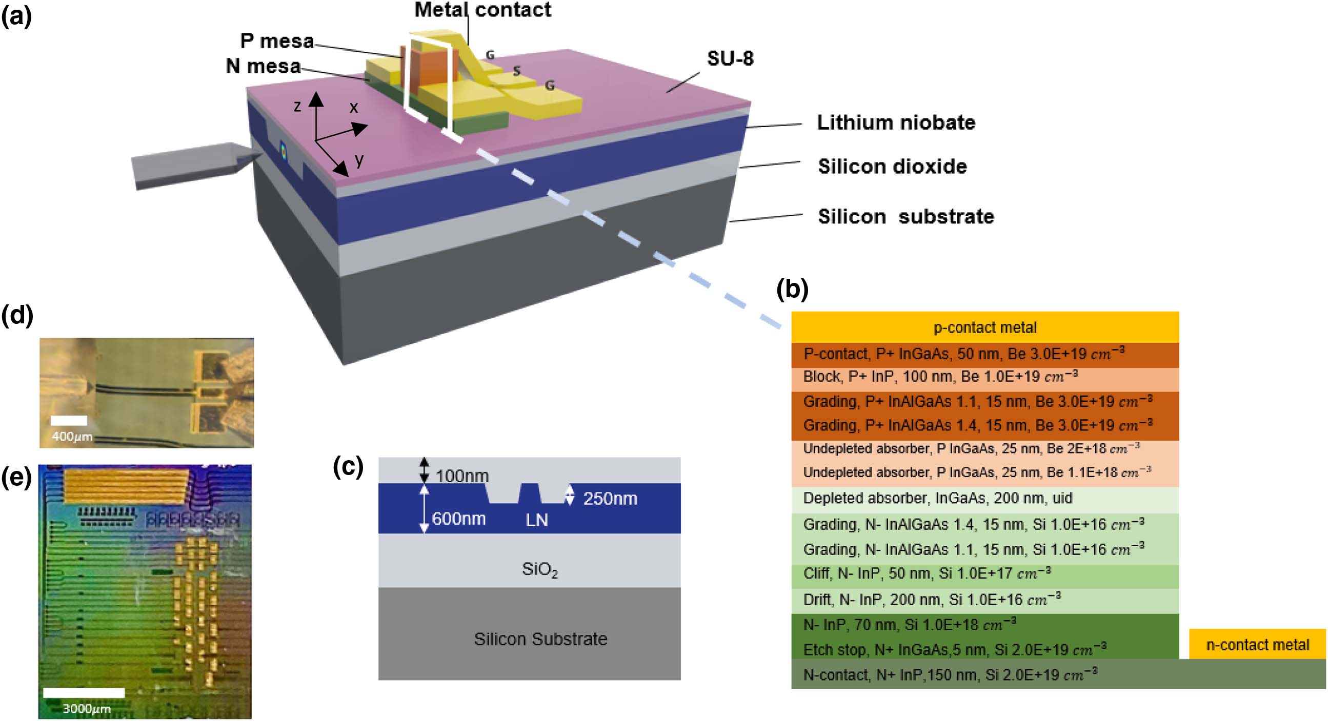
Figure 1.MUTC PDs integrated on TFLN. (a) Structural illustration. (b) Epitaxial structure of the n-down PD. (c) TFLN waveguide cross section. (d) Microscope image of a device under test with a lensed fiber and a radio frequency probe. (e) Microscope image of chip with integrated PDs.
![]()
Figure 2.Device simulations. (a) Calculation of transit time-limited bandwidth versus undepleted absorber thickness with total absorber thickness of 250 nm and a fixed drift layer thickness of 200 nm. Optical simulations of
As shown in Fig. 1(a) and in contrast to our previous work [5], we designed a structure that results in n down after bonding with the following benefits: the InP n-contact layer is transparent at the operating wavelength 1550 nm; a low sheet resistance in the contact layer can be achieved since high n-type doping levels (
Figure 1(c) shows a schematic of the TFLN waveguide which was optimized for photodiode integration. The total thickness of LN is 600 nm with the waveguide height being 250 nm. We deposited
Photodiodes were fabricated by first bonding a
3. DEVICE CHARACTERIZATION
A. DC Measurements
Dark current is an important figure of merit for PDs as it is one of the major sources for noise. The fact that the low dark current of our MUTC PD on a TFLN of 3 nA [Fig. 3(a)] is comparable to or lower than the dark current from similar PDs on a native substrate [12], indicates that the integration process did not degrade the performance.
![]()
Figure 3.DC measurements of MUTC photodiodes integrated on thin-film LN platform. (a) Dark current characteristics of a
The responsivity of the photodetectors was measured at 1550 nm by edge-coupling light into the TFLN waveguides. The external responsivity of the PDs was calculated by dividing the photocurrent by the optical power at the lensed fiber tip (measured by an optical power meter). For a
We also measured photocurrent versus optical power on a 20-μm wide and 30 μm-long PD. As shown in Fig. 3(b), the photocurrent was linear for input powers as high as 20 dBm.
B. Frequency Response
The 3-dB bandwidth was measured by a heterodyne setup. Two distributed feedback lasers with wavelengths near 1550 nm were used to generate a frequency tunable optical signal with near 100% modulation depth. The frequency of the beat signal is controlled by thermally tuning the wavelength of one laser, whereas the other laser remains at one stable wavelength. This optical signal was then directed to an erbium-doped fiber amplifier (EDFA) followed by a variable optical attenuator to control the amplitude of the optical signal. A single-mode tapered fiber was used to couple light into the TFLN waveguide. The fiber-to-waveguide alignment was performed using a six-axial stage. A GSG RF probe was used to extract the photocurrent by probing at the designed RF metal pads [Fig. 1(d)]. A semirigid coaxial cable was used to connect the RF probe with the bias tee. The RF signal was detected using a calibrated 50-Ω RF power meter with frequency range from DC to 110 GHz. The losses of the RF probe, semirigid coaxial cable, and bias tee were determined with a 110-GHz network analyzer and then subtracted from the measured data.
Figure 4(a) shows the bandwidth measurements of a
![]()
Figure 4.AC measurements of MUTC photodiodes integrated on thin-film LN. (a) Frequency responses of a
C. Eye Diagram
Digital data detection performance of the photodetectors was characterized by an eye diagram measurement. A non-return-to-zero on–off keyed pseudorandom bit sequence (PRBS) data pattern was generated by a PRBS generator at 40 Gbit/s. Figure 5(a) illustrates our experimental setup. An external cavity laser provided the optical signal for a commercial 40-GHz modulator. The 550-mV peak-to-peak signal from the PRBS generator was fed into the modulator biased at its quadrature point. The optical signal then went through an EDFA, a variable optical attenuator, and an optical filter with a 1-nm passband before being coupled into the TFLN waveguides. The electrical signal was extracted by an RF probe and went through a semirigid cable, a bias tee, and a coaxial cable before entering the 50-GHz sampling oscilloscope for the readout. It is worth mentioning that our PD handled sufficient photocurrent and provided a high signal-to-noise ratio for the oscilloscope, so no additional RF amplifier to boost up the electrical signal was necessary in the measurement.
![]()
Figure 5.Eye diagram measurement. (a) Measurement system setup. (b) Measured eye diagram for a commercial photodiode. (c) Measured eye diagram for an MUTC photodiode on TFLN with
We first measured the eye diagram of a commercial PD with a 40-GHz bandwidth shown in Fig. 5(b) as a reference. Figure 5(c) shows the measurement result of our
4. SUMMARY
In conclusion, we designed and fabricated MUTC photodiodes on TFLN waveguides. The internal responsivity for a high-speed photodiode with an 80-GHz bandwidth was 0.6 A/W. The dark current was as low as 3 nA. The fabrication process of our MUTC photodiodes was fully compatible with modulators and ring resonators on the same wafer. With excellent performance, our integrated MUTC photodiode could enable high-performance photonic integrated circuits on the LNOI platform.
Acknowledgment
Acknowledgment. The views, opinions, and/or findings expressed are those of the author(s) and should not be interpreted as representing the official views or policies of the Department of Defense or the U.S. Government. The authors from University of Virginia also acknowledge the Multidisciplinary University Research Initiative (MURI) program through the AFOSR, monitored by Dr. G. S. Pomrenke.
References
[1] M. Zhang, C. Wang, R. Cheng, A. Shams-Ansari, M. Lončar. Monolithic ultra-high-
[2] C. Wang, M. Zhang, X. Chen, M. Bertrand, A. Shams-Ansari, S. Chandrasekhar, P. Winzer, M. Lončar. Integrated lithium niobate electro-optic modulators operating at CMOS-compatible voltages. Nature, 562, 101-104(2018).
[3] D. Zhu, L. Shao, M. Yu, R. Cheng, B. Desiatov, C. J. Xin, Y. Hu, J. Holzgrafe, S. Ghosh, A. Shams-Ansari, E. Puma, N. Sinclair, C. Reimer, M. Zhang, M. Lončar. Integrated photonics on thin-film lithium niobate. Adv. Opt. Photon., 13, 242-352(2021).
[4] A. Shams-Ansari, D. Renaud, R. Cheng, L. Shao, L. He, D. Zhu, M. Yu, H. Grant, L. Johansson, M. Zhang, M. Lončar. Electrically pumped laser transmitter integrated on thin-film lithium niobate. Optica, 9, 408-411(2022).
[5] Q. Yu, J. Gao, N. Ye, B. Chen, K. Sun, L. Xie, K. Srinivasan, M. Zervas, G. Navickaite, M. Geiselmann, A. Beling. Heterogeneous photodiodes on silicon nitride waveguides. Opt. Express, 28, 14824-14830(2020).
[6] D. Maes, G. Roelkens, M. Zaknoune, C. O. de Beeck, S. Poelman, M. Billet, M. Muneeb, S. Lemey, E. Peytavit, B. Kuyken. Heterogeneous integration of uni-travelling-carrier photodiodes using micro-transfer-printing on a silicon-nitride platform. Conference on Lasers and Electro-Optics Europe and European Quantum Electronics Conference, 1(2021).
[7] P. Tiwari, P. Wen, S. Mauthe, M. Baumann, B. I. Bitachon, H. Schmid, J. Leuthold, K. E. Moselund. Butt-coupled III-V photodetector monolithically integrated on soi with data reception at 50 Gbps OOK. Optical Fiber Communication Conference, F2C.2(2021).
[8] A. Yi-Yan, W. K. Chan, T. J. Gmitter, L. T. Florez, J. L. Jackel, E. Yablonovitch, R. Bhat, J. P. Harbison. Grafted GaAs detectors on lithium niobite and glass waveguides. IEEE Photon. Technol. Lett., 1, 379-380(1989).
[9] B. Desiatov, M. Lončar. Silicon photodetector for integrated lithium niobate photonics. Appl. Phys. Lett., 115, 121108(2019).
[10] T. Ishibashi, Y. Muramoto, T. Yoshimatsu, H. Ito. Unitraveling-carrier photodiodes for terahertz applications. IEEE J. Sel. Top. Quantum Electron., 20, 3804210(2014).
[11] A. Beling, X. Xie, J. C. Campbell. High-power, high-linearity photodiodes. Optica, 3, 328-338(2016).
[12] Q. Li, K. Sun, K. Li, Q. Yu, P. Runge, W. Ebert, A. Beling, J. C. Campbell. High-power evanescently coupled waveguide MUTC photodiode with <105-GHz bandwidth. J. Lightwave Technol., 35, 4752-4757(2017).
[13] X. Xie, Q. Zhou, E. Norberg, M. Jacob-Mitos, Y. Chen, A. Ramaswamy, G. Fish, J. E. Bowers, J. Campbell, A. Beling. Heterogeneously integrated waveguide-coupled photodiodes on SOI with 12 dBm output power at 40 GHz. Optical Fiber Communication Conference, Th5B.7(2015).


Set citation alerts for the article
Please enter your email address

© Copyright 2018-2021 | Chinese Laser Press. All Rights Reserved 沪ICP备15018463号-20