Contents


2020
Volume: 8 Issue 4
24 Article(s)
Export citation format
Reviews
Fiber Optics and Optical Communications
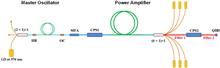
Experimental study of mode distortion induced by stimulated Raman scattering in high-power fiber amplifiers
Qiuhui Chu, Qiang Shu, Zeng Chen, Fengyun Li... and Rumao Tao|Show fewer author(s)
The experimental investigation of mode distortion induced by stimulated Raman scattering (SRS) in a high-power fiber amplifier, which includes the evolutions of optical spectra, spatial beam profiles, and time-frequency characteristics, has been carried out in detail. Temporal-frequency characteristics have been studied for the first time, to the best of our knowledge, by using a low-speed camera and high-speed photodiode traces, which revealed that temporal-frequency characteristics of SRS-induced mode distortion are different from traditional dynamic mode instability (MI). The experimental results show that the output beam profile remains stable before the mode distortion occurs and fluctuates obviously after the onset of SRS-induced MI but on a time scale of seconds, which is much lower than that of Yb-gain-induced MI featuring millisecond-level beam profile fluctuation. It also shows that the mode distortion became measurable in company with the onset of inter-mode four-wave mixing (IM-FWM) when the ratio of Raman light reaches 3%; further, the beam quality factor M2 degrades gradually from 1.4 to 2.1 as the ratio of Raman light increases. The mode distortion is accompanied by an obvious temperature increase of the output passive fiber, which further confirms that the mode distortion originates from SRS. The cause of the mode distortion induced by SRS has been explained in the context of core-pumped SRS effect, and the investigation on the accompanying IM-FWM effect indicates that the main content of the SRS-induced high-order mode is the LP21 mode.The experimental investigation of mode distortion induced by stimulated Raman scattering (SRS) in a high-power fiber amplifier, which includes the evolutions of optical spectra, spatial beam profiles, and time-frequency characteristics, has been carried out in detail. Temporal-frequency characteristics have been studied for the first time, to the best of our knowledge, by using a low-speed camera and high-speed photodiode traces, which revealed that temporal-frequency characteristics of SRS-induced mode distortion are different from traditional dynamic mode instability (MI). The experimental results show that the output beam profile remains stable before the mode distortion occurs and fluctuates obviously after the onset of SRS-induced MI but on a time scale of seconds, which is much lower than that of Yb-gain-induced MI featuring millisecond-level beam profile fluctuation. It also shows that the mode distortion became measurable in company with the onset of inter-mode four-wave mixing (IM-FWM) when the ratio of Raman light reaches 3%; further, the beam quality factor
Photonics Research
- Publication Date: Apr. 01, 2020
- Vol. 8, Issue 4, 595 (2020)


Optical and Photonic Materials
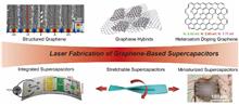
Laser fabrication of graphene-based supercapacitors
Xiu-Yan Fu, Zhao-Di Chen, Dong-Dong Han, Yong-Lai Zhang... and Hong-Bo Sun|Show fewer author(s)
Supercapacitors (SCs) have broad applications in wearable electronics (e.g., e-skin, robots). Recently, graphene-based supercapacitors (G-SCs) have attracted extensive attention for their excellent flexibility and electrochemical performance. Laser fabrication of G-SCs exhibits obvious superiority because of the simple procedures and integration compatibility with future electronics. Here, we comprehensively summarize the state-of-the-art advancements in laser-assisted preparation of G-SCs, including working mechanisms, fabrication procedures, and unique characteristics. In the working mechanism section, electric double-layer capacitors and pseudo-capacitors are introduced. The latest advancements in this field are comprehensively summarized, including laser reduction of graphene oxides, laser treatment of graphene prepared from chemical vapor deposition, and laser-induced graphene. In addition, the unique characteristics of laser-enabled G-SCs, such as structured graphene, graphene hybrids, and heteroatom doping graphene-related electrodes, are presented. Subsequently, laser-enabled miniaturized, stretchable, and integrated G-SCs are also discussed. It is anticipated that laser fabrication of G-SCs holds great promise for developing future energy storage devices.Supercapacitors (SCs) have broad applications in wearable electronics (e.g., e-skin, robots). Recently, graphene-based supercapacitors (G-SCs) have attracted extensive attention for their excellent flexibility and electrochemical performance. Laser fabrication of G-SCs exhibits obvious superiority because of the simple procedures and integration compatibility with future electronics. Here, we comprehensively summarize the state-of-the-art advancements in laser-assisted preparation of G-SCs, including working mechanisms, fabrication procedures, and unique characteristics. In the working mechanism section, electric double-layer capacitors and pseudo-capacitors are introduced. The latest advancements in this field are comprehensively summarized, including laser reduction of graphene oxides, laser treatment of graphene prepared from chemical vapor deposition, and laser-induced graphene. In addition, the unique characteristics of laser-enabled G-SCs, such as structured graphene, graphene hybrids, and heteroatom doping graphene-related electrodes, are presented. Subsequently, laser-enabled miniaturized, stretchable, and integrated G-SCs are also discussed. It is anticipated that laser fabrication of G-SCs holds great promise for developing future energy storage devices..
Photonics Research
- Publication Date: Apr. 01, 2020
- Vol. 8, Issue 4, 577 (2020)
Optical Devices
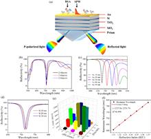
Photonic cavity enhanced high-performance surface plasmon resonance biosensor
Gui-Shi Liu, Xin Xiong, Shiqi Hu, Weicheng Shi... and Zhe Chen|Show fewer author(s)
Herein we propose a novel strategy to enhance surface plasmon resonance (SPR) by introducing a photonic cavity into a total-internal-reflection architecture. The photonic cavity, which is comprised of a highly reflective photonic crystal (PC), defect layers, and a gold (Au) film, enables Fabry–Perot (FP) resonances in the defect layers and therefore narrows the SPR resonance width in the metallic surface as well as increases the electric field intensity and penetration depth in the evanescent region. The fabricated sensor exhibits a 5.7-fold increase in the figure of merit and a higher linear coefficient as compared with the conventional Au-SPR sensor. The demonstrated PC/FP cavity/metal structure presents a new design philosophy for SPR performance enhancement.Herein we propose a novel strategy to enhance surface plasmon resonance (SPR) by introducing a photonic cavity into a total-internal-reflection architecture. The photonic cavity, which is comprised of a highly reflective photonic crystal (PC), defect layers, and a gold (Au) film, enables Fabry–Perot (FP) resonances in the defect layers and therefore narrows the SPR resonance width in the metallic surface as well as increases the electric field intensity and penetration depth in the evanescent region. The fabricated sensor exhibits a 5.7-fold increase in the figure of merit and a higher linear coefficient as compared with the conventional Au-SPR sensor. The demonstrated PC/FP cavity/metal structure presents a new design philosophy for SPR performance enhancement..
Photonics Research
- Publication Date: Mar. 06, 2020
- Vol. 8, Issue 4, 448 (2020)
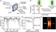
Real-time monitoring of hydrogel phase transition in an ultrahigh Q microbubble resonator
Daquan Yang, Aiqiang Wang, Jin-Hui Chen, Xiao-Chong Yu... and Yun-Feng Xiao|Show fewer author(s)
The ability to sense dynamic biochemical reactions and material processes is particularly crucial for a wide range of applications, such as early-stage disease diagnosis and biomedicine development. Optical microcavities-based label-free biosensors are renowned for ultrahigh sensitivities, and the detection limit has reached a single nanoparticle/molecule level. In particular, a microbubble resonator combined with an ultrahigh quality factor (Q) and inherent microfluidic channel is an intriguing platform for optical biosensing in an aqueous environment. In this work, an ultrahigh Q microbubble resonator-based sensor is used to characterize dynamic phase transition of a thermosensitive hydrogel. Experimentally, by monitoring resonance wavelength shift and linewidth broadening, we (for the first time to our knowledge) reveal that the refractive index is increased and light scattering is enhanced simultaneously during the hydrogel hydrophobic transition process. The platform demonstrated here paves the way to microfluidical biochemical dynamic detection and can be further adapted to investigating single-molecule kinetics.The ability to sense dynamic biochemical reactions and material processes is particularly crucial for a wide range of applications, such as early-stage disease diagnosis and biomedicine development. Optical microcavities-based label-free biosensors are renowned for ultrahigh sensitivities, and the detection limit has reached a single nanoparticle/molecule level. In particular, a microbubble resonator combined with an ultrahigh quality factor (
Photonics Research
- Publication Date: Mar. 23, 2020
- Vol. 8, Issue 4, 497 (2020)
Enhancing sensing capacity of terahertz metamaterial absorbers with a surface-relief design
Wei Wang, Fengping Yan, Siyu Tan, Haisu Li... and Yafei Hou|Show fewer author(s)
Metamaterial absorbers (MAs) serve as important electromagnetic wave-absorbing devices that have captured the attention of researchers for a long term. Functioning as sensitive detectors to determine perturbations in an ambient environment is another significant subsidiary function. Here, we theoretically propose an optimized fabrication method to implement terahertz MAs with fewer steps and also evaluate both absorption and sensing performances of such MAs realized by the new method. Simulation findings demonstrate that such MAs can basically maintain the original absorption features perfectly, including near-complete absorption at resonance as well as strong robustness to wide incident angles. Specifically, the full width at half-maximum and quality factor of the absorption resonances attenuate less than 26% and 8% with this new method, remaining in the ranges of ~0.03–0.04 THz and ~20–27 for two selected example MAs. More significantly, sensing capacities of this type of MA, in terms of maximum detection range (enhancing at least 9%), observable spectral modulation (increasing at least 6.3%), and refractive index sensitivity, are improved to a large extent because of more intense coupling between resonant field and matter in the case of surface-relief MAs. This stronger coupling results from exposing more spots of the resonantly high field to direct contact with an approaching analyte, which is illustrated by field profiles of the MAs at resonance in this work. Additionally, other desirable absorber features are also explored with such MAs, like functioning as building blocks to configure multiband MAs and strong robustness against fabrication errors. Such new-style terahertz MAs shown in the paper, acting as good examples, not only prove that terahertz MAs can be fabricated by the proposed time- and cost-saving route in contrast to the traditional MA fabrication process, but also can serve as novel platforms to explore other intriguing terahertz photonic effects, such as the field enhancement effect.Metamaterial absorbers (MAs) serve as important electromagnetic wave-absorbing devices that have captured the attention of researchers for a long term. Functioning as sensitive detectors to determine perturbations in an ambient environment is another significant subsidiary function. Here, we theoretically propose an optimized fabrication method to implement terahertz MAs with fewer steps and also evaluate both absorption and sensing performances of such MAs realized by the new method. Simulation findings demonstrate that such MAs can basically maintain the original absorption features perfectly, including near-complete absorption at resonance as well as strong robustness to wide incident angles. Specifically, the full width at half-maximum and quality factor of the absorption resonances attenuate less than 26% and 8% with this new method, remaining in the ranges of
Photonics Research
- Publication Date: Mar. 24, 2020
- Vol. 8, Issue 4, 519 (2020)

Mid-infrared chalcogenide microfiber knot resonators
Yu Xie, Dawei Cai, Hao Wu, Jing Pan... and Limin Tong|Show fewer author(s)
A novel type of mid-IR microresonator, the chalcogenide glass (ChG) microfiber knot resonator (MKR), is demonstrated, showing easy fabrication, fiber-compatible features, resonance tunability, and high robustness. ChG microfibers with typical diameters around 3 μm are taper-drawn from As2S3 glass fibers and assembled into MKRs in liquid without surface damage. The measured Q factor of a typical 824 μm diameter ChG MKR is about 2.84×10⁴ at the wavelength of 4469.14 nm. The free spectral range (FSR) of the MKR can be tuned from 2.0 nm (28.4 GHz) to 9.6 nm (135.9 GHz) by tightening the knot structure in liquid. Benefitting from the high thermal expansion coefficient of As2S3 glass, the MKR exhibits a thermal tuning rate of 110 pm·°C?1 at the resonance peak. When embedded in polymethyl methacrylate (PMMA) film, a 551 μm diameter MKR retains a Q factor of 1.1×10⁴. The ChG MKRs demonstrated here are highly promising for resonator-based optical technologies and applications in the mid-IR spectral range.A novel type of mid-IR microresonator, the chalcogenide glass (ChG) microfiber knot resonator (MKR), is demonstrated, showing easy fabrication, fiber-compatible features, resonance tunability, and high robustness. ChG microfibers with typical diameters around 3 μm are taper-drawn from
Photonics Research
- Publication Date: Apr. 01, 2020
- Vol. 8, Issue 4, 616 (2020)
Physical Optics
Self-accelerated optical activity in free space induced by the Gouy phase
Peng Li, Xinhao Fan, Dongjing Wu, Sheng Liu... and Jianlin Zhao|Show fewer author(s)
Optical activity (OA) is the rotation of the polarization orientation of the linearly polarized light as it travels through certain materials that are of mirror asymmetry, including gases or solutions of chiral molecules such as sugars and proteins, as well as metamaterials. The necessary condition for achieving OA is the birefringence of two circular polarizations in material. Here, we propose a new kind of self-accelerated OA in free space, based on the intrinsic Gouy phase induced mode birefringence of two kinds of quasi-non-diffracting beams. We provide a detailed insight into this kind of self-accelerated OA by analyzing angular parameters, including angular direction, velocity, acceleration, and even the polarization transformation trajectory. As the Gouy phase exists for any wave, this kind of self-accelerated OA can be implemented in other waves beyond optics, from acoustic and elastic waves to matter waves.Optical activity (OA) is the rotation of the polarization orientation of the linearly polarized light as it travels through certain materials that are of mirror asymmetry, including gases or solutions of chiral molecules such as sugars and proteins, as well as metamaterials. The necessary condition for achieving OA is the birefringence of two circular polarizations in material. Here, we propose a new kind of self-accelerated OA in free space, based on the intrinsic Gouy phase induced mode birefringence of two kinds of quasi-non-diffracting beams. We provide a detailed insight into this kind of self-accelerated OA by analyzing angular parameters, including angular direction, velocity, acceleration, and even the polarization transformation trajectory. As the Gouy phase exists for any wave, this kind of self-accelerated OA can be implemented in other waves beyond optics, from acoustic and elastic waves to matter waves..
Photonics Research
- Publication Date: Mar. 23, 2020
- Vol. 8, Issue 4, 475 (2020)
Super-bunched focusing with chirped random-phase gratings
Lu Zhang, Dongxu Zhou, Yiping Lu, Hongzhi Zhang, and Guoquan Zhang
Chirped random-phase gratings are designed to produce experimentally a super-bunched focusing effect with a high bunching peak value of g(2)(0)=15.38±0.05 and a high visibility of 92.5%, greatly surpassing the theoretical bunching peak of 2 of thermal light. Both slit-width-chirped and period-chirped random-phase gratings are studied theoretically and experimentally. The full width at half-maximum of the super-bunched curve decreases significantly with an increase in the slit number, focusing the photon pairs within a decreasing spot size. This super-bunched focusing effect can be useful for improving the resolution and the visibility of the correlation image simultaneously.Chirped random-phase gratings are designed to produce experimentally a super-bunched focusing effect with a high bunching peak value of
Photonics Research
- Publication Date: Mar. 23, 2020
- Vol. 8, Issue 4, 503 (2020)
Research Articles
Holography, Gratings, and Diffraction
Revealing the underlying mechanisms behind TE extraordinary THz transmission
Suzanna Freer, Miguel Camacho, Sergei A. Kuznetsov, Rafael R. Boix... and Miguel Navarro-Cía|Show fewer author(s)
Transmission through seemingly opaque surfaces, so-called extraordinary transmission, provides an exciting platform for strong light–matter interaction, spectroscopy, optical trapping, and color filtering. Much of the effort has been devoted to understanding and exploiting TM extraordinary transmission, while TE anomalous extraordinary transmission has been largely omitted in the literature. This is regrettable from a practical point of view since the stronger dependence of the TE anomalous extraordinary transmission on the array’s substrate provides additional design parameters for exploitation. To provide high-performance and cost-effective applications based on TE anomalous extraordinary transmission, a complete physical insight about the underlying mechanisms of the phenomenon must be first laid down. To this end, resorting to a combined methodology including quasi-optical terahertz (THz) time-domain measurements, full-wave simulations, and method of moments analysis, subwavelength slit arrays under s-polarized illumination are studied here, filling the void in the current literature. We believe this work unequivocally reveals the leaky-wave role of the grounded-dielectric slab mode mediating in TE anomalous extraordinary transmission and provides the necessary framework to design practical high-performance THz components and systems.Transmission through seemingly opaque surfaces, so-called extraordinary transmission, provides an exciting platform for strong light–matter interaction, spectroscopy, optical trapping, and color filtering. Much of the effort has been devoted to understanding and exploiting TM extraordinary transmission, while TE anomalous extraordinary transmission has been largely omitted in the literature. This is regrettable from a practical point of view since the stronger dependence of the TE anomalous extraordinary transmission on the array’s substrate provides additional design parameters for exploitation. To provide high-performance and cost-effective applications based on TE anomalous extraordinary transmission, a complete physical insight about the underlying mechanisms of the phenomenon must be first laid down. To this end, resorting to a combined methodology including quasi-optical terahertz (THz) time-domain measurements, full-wave simulations, and method of moments analysis, subwavelength slit arrays under s-polarized illumination are studied here, filling the void in the current literature. We believe this work unequivocally reveals the leaky-wave role of the grounded-dielectric slab mode mediating in TE anomalous extraordinary transmission and provides the necessary framework to design practical high-performance THz components and systems..
Photonics Research
- Publication Date: Mar. 03, 2020
- Vol. 8, Issue 4, 430 (2020)
Image Processing and Image Analysis
Wide-field ophthalmic space-division multiplexing optical coherence tomography
Jason Jerwick, Yongyang Huang, Zhao Dong, Adrienne Slaudades... and Chao Zhou|Show fewer author(s)
High-speed ophthalmic optical coherence tomography (OCT) systems are of interest because they allow rapid, motion-free, and wide-field retinal imaging. Space-division multiplexing optical coherence tomography (SDM-OCT) is a high-speed imaging technology that takes advantage of the long coherence length of microelectromechanical vertical cavity surface emitting laser sources to multiplex multiple images along a single imaging depth. We demonstrate wide-field retinal OCT imaging, acquired at an effective A-scan rate of 800,000 A-scans/s with volumetric images covering up to 12.5 mm×7.4 mm on the retina and captured in less than 1 s. A clinical feasibility study was conducted to compare the ophthalmic SDM-OCT with commercial OCT systems, illustrating the high-speed capability of SDM-OCT in a clinical setting.High-speed ophthalmic optical coherence tomography (OCT) systems are of interest because they allow rapid, motion-free, and wide-field retinal imaging. Space-division multiplexing optical coherence tomography (SDM-OCT) is a high-speed imaging technology that takes advantage of the long coherence length of microelectromechanical vertical cavity surface emitting laser sources to multiplex multiple images along a single imaging depth. We demonstrate wide-field retinal OCT imaging, acquired at an effective A-scan rate of 800,000 A-scans/s with volumetric images covering up to
Photonics Research
- Publication Date: Mar. 31, 2020
- Vol. 8, Issue 4, 539 (2020)
Integrated Optics
Inverse design of digital nanophotonic devices using the adjoint method | On the Cover
Kaiyuan Wang, Xinshu Ren, Weijie Chang, Longhui Lu... and Minming Zhang|Show fewer author(s)
A high-efficiency inverse design of “digital” subwavelength nanophotonic devices using the adjoint method is proposed. We design a single-mode 3 dB power divider and a dual-mode demultiplexer to demonstrate the efficiency of the proposed inverse design approach, called the digitized adjoint method, for single- and dual-object optimization, respectively. The optimization comprises three stages: 1) continuous variation for an “analog” pattern; 2) forced permittivity biasing for a “quasi-digital” pattern; and 3) a multilevel digital pattern. Compared with the conventional brute-force method, the proposed method can improve design efficiency by about five times, and the performance optimization can reach approximately the same level. The method takes advantages of adjoint sensitivity analysis and digital subwavelength structure and creates a new way for the efficient and high-performance design of compact digital subwavelength nanophotonic devices, which could overcome the efficiency bottleneck of the brute-force method, which is restricted by the number of pixels of a digital pattern, and improve the device performance by extending a conventional binary pattern to a multilevel one.A high-efficiency inverse design of “digital” subwavelength nanophotonic devices using the adjoint method is proposed. We design a single-mode 3 dB power divider and a dual-mode demultiplexer to demonstrate the efficiency of the proposed inverse design approach, called the digitized adjoint method, for single- and dual-object optimization, respectively. The optimization comprises three stages: 1) continuous variation for an “analog” pattern; 2) forced permittivity biasing for a “quasi-digital” pattern; and 3) a multilevel digital pattern. Compared with the conventional brute-force method, the proposed method can improve design efficiency by about five times, and the performance optimization can reach approximately the same level. The method takes advantages of adjoint sensitivity analysis and digital subwavelength structure and creates a new way for the efficient and high-performance design of compact digital subwavelength nanophotonic devices, which could overcome the efficiency bottleneck of the brute-force method, which is restricted by the number of pixels of a digital pattern, and improve the device performance by extending a conventional binary pattern to a multilevel one..
Photonics Research
- Publication Date: Mar. 24, 2020
- Vol. 8, Issue 4, 528 (2020)
Versatile on-chip light coupling and (de)multiplexing from arbitrary polarizations to controlled waveguide modes using an integrated dielectric metasurface
Yuan Meng, Zhoutian Liu, Zhenwei Xie, Ride Wang... and Xiaocong Yuan|Show fewer author(s)
Metasurfaces have found broad applicability in free-space optics, while its potential to tailor guided waves remains barely explored. By synergizing the Jones matrix model with generalized Snell’s law under the phase-matching condition, we propose a universal design strategy for versatile on-chip mode-selective coupling with polarization sensitivity, multiple working wavelengths, and high efficiency concurrently. The coupling direction, operation frequency, and excited mode type can be designed at will for arbitrary incident polarizations, outperforming previous technology that only works for specific polarizations and lacks versatile mode controllability. Here, using silicon-nanoantenna-patterned silicon-nitride photonic waveguides, we numerically demonstrate a set of chip-scale optical couplers around 1.55 μm, including mode-selective directional couplers with high coupling efficiency over 57% and directivity about 23 dB. Polarization and wavelength demultiplexer scenarios are also proposed with 67% maximum efficiency and an extinction ratio of 20 dB. Moreover, a chip-integrated twisted light generator, coupling free-space linear polarization into an optical vortex carrying 1? orbital angular momentum (OAM), is also reported to validate the mode-control flexibility. This comprehensive method may motivate compact wavelength/polarization (de)multiplexers, multifunctional mode converters, on-chip OAM generators for photonic integrated circuits, and high-speed optical telecommunications.Metasurfaces have found broad applicability in free-space optics, while its potential to tailor guided waves remains barely explored. By synergizing the Jones matrix model with generalized Snell’s law under the phase-matching condition, we propose a universal design strategy for versatile on-chip mode-selective coupling with polarization sensitivity, multiple working wavelengths, and high efficiency concurrently. The coupling direction, operation frequency, and excited mode type can be designed at will for arbitrary incident polarizations, outperforming previous technology that only works for specific polarizations and lacks versatile mode controllability. Here, using silicon-nanoantenna-patterned silicon-nitride photonic waveguides, we numerically demonstrate a set of chip-scale optical couplers around 1.55 μm, including mode-selective directional couplers with high coupling efficiency over 57% and directivity about 23 dB. Polarization and wavelength demultiplexer scenarios are also proposed with 67% maximum efficiency and an extinction ratio of 20 dB. Moreover, a chip-integrated twisted light generator, coupling free-space linear polarization into an optical vortex carrying
Photonics Research
- Publication Date: Apr. 01, 2020
- Vol. 8, Issue 4, 564 (2020)
Lasers and Laser Optics
Passively Q-switched and femtosecond mode-locked erbium-doped fiber laser based on a 2D palladium disulfide (PdS2) saturable absorber
Ping Kwong Cheng, Chun Yin Tang, Xin Yu Wang, Long-Hui Zeng, and Yuen Hong Tsang
Stable Q-switched and mode-locked erbium-doped fiber lasers (EDFLs) are first demonstrated by using the novel layered palladium disulfide (PdS2), a new member of group 10 transition metal dichalcogenides (TMDs)-based saturable absorbers (SAs). Self-started Q-switched operation at 1567 nm was achieved with a threshold pump power of 50.6 mW. The modulation ranges of pulse duration and repetition rate were characterized as 12.6–4.5 μs and 17.2–26.0 kHz, respectively. Meanwhile, a mode-locked EDFL was also obtained with a pump power threshold of 106.4 mW. The achieved pulse duration is 803 fs, corresponding to a center wavelength of 1565.8 nm and 4.48 nm 3 dB bandwidth. To the best of our knowledge, the achieved pulse duration of the mode-locked EDFL in this work is the narrowest compared with all other group 10 TMD SA-based lasers.Stable
Photonics Research
- Publication Date: Mar. 24, 2020
- Vol. 8, Issue 4, 511 (2020)
Laser-induced rotary micromotor with high energy conversion efficiency
Yu Zhang, Siyu Lin, Zhihai Liu, Yaxun Zhang... and Libo Yuan|Show fewer author(s)
Light is a precious resource that nature has given to human beings. Converting green, recyclable light energy into the mechanical energy of a micromotor is undoubtedly an exciting challenge. However, the performance of current light-induced micromotor devices is unsatisfactory, as the light-to-work conversion efficiency is only 10?15–10?12. In this paper, we propose and demonstrate a laser-induced rotary micromotor operated by Δα-type photopheresis in pure liquid glycerol, whose energy conversion ratio reaches as high as 10?9, which is 3–6 orders of magnitude higher than that of previous light-induced micromotor devices. In addition, we operate the micromotor neither with a light field carrying angular momentum nor with a rotor with a special rotating symmetrical shape. We just employ an annular-core fiber to configure a conical-shaped light field and select a piece of graphite sheet (with an irregular shape) as the micro-rotor. The Δα-type photophoretic force introduced by the conical-shaped light field drives the rotation of the graphite sheet. We achieve a rotation rate up to 818.2 r/min, which can be controlled by tuning the incident laser power. This optical rotary micromotor is available for twisting macromolecules or generating vortex and shear force in a medium at the nanoscale.Light is a precious resource that nature has given to human beings. Converting green, recyclable light energy into the mechanical energy of a micromotor is undoubtedly an exciting challenge. However, the performance of current light-induced micromotor devices is unsatisfactory, as the light-to-work conversion efficiency is only
Photonics Research
- Publication Date: Mar. 25, 2020
- Vol. 8, Issue 4, 534 (2020)
Nonlinear Optics
Brillouin wavelength-selective all-optical polarization conversion
Diego Samaniego, and Borja Vidal
The manipulation of the polarization properties of light in guided media is crucial in many classical and quantum optical systems. However, the capability of current technology to finely define the state of polarization of particular wavelengths is far from the level of maturity in amplitude control. Here, we introduce a light-by-light polarization control mechanism with wavelength selectivity based on the change of the phase retardance by means of stimulated Brillouin scattering. Experiments show that any point on the Poincaré sphere can be reached from an arbitrary input state of polarization with little variation of the signal amplitude (2.5 dB). Unlike other Brillouin processing schemes, the degradation of the noise figure is small (1.5 dB for a full 2π rotation). This all-optical polarization controller can forge the development of new polarization-based techniques in optical communication, laser engineering, sensing, quantum systems, and light-based probing of chemical and biological systems.The manipulation of the polarization properties of light in guided media is crucial in many classical and quantum optical systems. However, the capability of current technology to finely define the state of polarization of particular wavelengths is far from the level of maturity in amplitude control. Here, we introduce a light-by-light polarization control mechanism with wavelength selectivity based on the change of the phase retardance by means of stimulated Brillouin scattering. Experiments show that any point on the Poincaré sphere can be reached from an arbitrary input state of polarization with little variation of the signal amplitude (
Photonics Research
- Publication Date: Mar. 06, 2020
- Vol. 8, Issue 4, 440 (2020)
Optical and Photonic Materials
Individually resolved luminescence from closely stacked GaN/AlN quantum wells
Bowen Sheng, Gordon Schmidt, Frank Bertram, Peter Veit... and Xinqiang Wang|Show fewer author(s)
Investigating closely stacked GaN/AlN multiple quantum wells (MQWs) by means of cathodoluminescence spectroscopy directly performed in a scanning transmission electron microscope, we have reached an ultimate spatial resolution of σCL=1.8 nm. The pseudomorphically grown MQWs with high interface quality emit in the deep ultraviolet spectral range. Demonstrating the capability of resolving the 10.8 nm separated, ultra-thin quantum wells, a cathodoluminescence profile was taken across individual ones. Applying a diffusion model of excitons generated by a Gaussian-broadened electron probe, the spatial resolution of cathodoluminescence down to the free exciton Bohr radius scale has been determined.Investigating closely stacked GaN/AlN multiple quantum wells (MQWs) by means of cathodoluminescence spectroscopy directly performed in a scanning transmission electron microscope, we have reached an ultimate spatial resolution of
Photonics Research
- Publication Date: Apr. 01, 2020
- Vol. 8, Issue 4, 610 (2020)
Optoelectronics
Improved performance of UVC-LEDs by combination of high-temperature annealing and epitaxially laterally overgrown AlN/sapphire
Norman Susilo, Eviathar Ziffer, Sylvia Hagedorn, Leonardo Cancellara... and Michael Kneissl|Show fewer author(s)
We report on the performance of AlGaN-based deep ultraviolet light-emitting diodes (UV-LEDs) emitting at 265 nm grown on stripe-patterned high-temperature annealed (HTA) epitaxially laterally overgrown (ELO) aluminium nitride (AlN)/sapphire templates. For this purpose, the structural and electro-optical properties of ultraviolet-c light-emitting diodes (UVC-LEDs) on as-grown and on HTA planar AlN/sapphire as well as ELO AlN/sapphire with and without HTA are investigated and compared. Cathodoluminescence measurements reveal dark spot densities of 3.5×109 cm?2, 1.1×109 cm?2, 1.4×109 cm?2, and 0.9×109 cm?2 in multiple quantum well samples on as-grown planar AlN/sapphire, HTA planar AlN/sapphire, ELO AlN/sapphire, and HTA ELO AlN/sapphire, respectively, and are consistent with the threading dislocation densities determined by transmission electron microscopy (TEM) and high-resolution X-ray diffraction rocking curve. The UVC-LED performance improves with the reduction of the threading dislocation densities (TDDs). The output powers (measured on-wafer in cw operation at 20 mA) of the UV-LEDs emitting at 265 nm were 0.03 mW (planar AlN/sapphire), 0.8 mW (planar HTA AlN/sapphire), 0.9 mW (ELO AlN/sapphire), and 1.1 mW (HTA ELO AlN/sapphire), respectively. Furthermore, Monte Carlo ray-tracing simulations showed a 15% increase in light-extraction efficiency due to the voids formed in the ELO process. These results demonstrate that HTA ELO AlN/sapphire templates provide a viable approach to increase the efficiency of UV-LEDs, improving both the internal quantum efficiency and the light-extraction efficiency.We report on the performance of AlGaN-based deep ultraviolet light-emitting diodes (UV-LEDs) emitting at 265 nm grown on stripe-patterned high-temperature annealed (HTA) epitaxially laterally overgrown (ELO) aluminium nitride (AlN)/sapphire templates. For this purpose, the structural and electro-optical properties of ultraviolet-c light-emitting diodes (UVC-LEDs) on as-grown and on HTA planar AlN/sapphire as well as ELO AlN/sapphire with and without HTA are investigated and compared. Cathodoluminescence measurements reveal dark spot densities of
Photonics Research
- Publication Date: Apr. 01, 2020
- Vol. 8, Issue 4, 589 (2020)
Quantum Optics
Frequency-tuning-induced state transfer in optical microcavities
Xu-Sheng Xu, Hao Zhang, Xiang-Yu Kong, Min Wang, and Gui-Lu Long
Quantum state transfer in optical microcavities plays an important role in quantum information processing and is essential in many optical devices such as optical frequency converters and diodes. Existing schemes are effective and realized by tuning the coupling strengths between modes. However, such approaches are severely restricted due to the small amount of strength that can be tuned and the difficulty performing the tuning in some situations, such as in an on-chip microcavity system. Here we propose a novel approach that realizes the state transfer between different modes in optical microcavities by tuning the frequency of an intermediate mode. We show that for typical functions of frequency tuning, such as linear and periodic functions, the state transfer can be realized successfully with different features. To optimize the process, we use the gradient descent technique to find an optimal tuning function for a fast and perfect state transfer. We also showed that our approach has significant nonreciprocity with appropriate tuning variables, where one can unidirectionally transfer a state from one mode to another, but the inverse direction transfer is forbidden. This work provides an effective method for controlling the multimode interactions in on-chip optical microcavities via simple operations, and it has practical applications in all-optical devices.Quantum state transfer in optical microcavities plays an important role in quantum information processing and is essential in many optical devices such as optical frequency converters and diodes. Existing schemes are effective and realized by tuning the coupling strengths between modes. However, such approaches are severely restricted due to the small amount of strength that can be tuned and the difficulty performing the tuning in some situations, such as in an on-chip microcavity system. Here we propose a novel approach that realizes the state transfer between different modes in optical microcavities by tuning the frequency of an intermediate mode. We show that for typical functions of frequency tuning, such as linear and periodic functions, the state transfer can be realized successfully with different features. To optimize the process, we use the gradient descent technique to find an optimal tuning function for a fast and perfect state transfer. We also showed that our approach has significant nonreciprocity with appropriate tuning variables, where one can unidirectionally transfer a state from one mode to another, but the inverse direction transfer is forbidden. This work provides an effective method for controlling the multimode interactions in on-chip optical microcavities via simple operations, and it has practical applications in all-optical devices..
Photonics Research
- Publication Date: Mar. 23, 2020
- Vol. 8, Issue 4, 490 (2020)
Superconducting nanowire multi-photon detectors enabled by current reservoirs
Kai Zou, Yun Meng, Zhao Wang, and Xiaolong Hu
Single-photon detectors are ubiquitous devices in quantum-photonic-based communication, computation, metrology, and sensing. In these applications, N-fold coincidence photon counting is often needed, for example, to characterize entanglement. However, N-fold coincidence photon counting typically requires N individual single-photon detectors and associated bias and readout electronics, and these resources could become prohibitive if N goes large and the detectors need to work at cryogenic temperatures. Here, to break this limit on N, we propose a device architecture based on N cascaded photosensitive superconducting nanowires and one wider nanowire that functions as a current reservoir. We show that by strategically designing the device, the network of these superconducting nanowires can work in a synergic manner as an n-photon detector, where n can be from 1 to N, depending on the bias conditions. We therefore name the devices of this type superconducting nanowire multi-photon detectors (SNMPDs). In addition to its simple one-port bias and readout circuitry, the coincidences are counted internally in the detector, eliminating the need for external multi-channel, time-correlated pulse counters. We believe that the SNMPDs proposed in this work could open avenues towards conveniently measuring high-order temporal correlations of light and characterizing multi-photon entanglement.Single-photon detectors are ubiquitous devices in quantum-photonic-based communication, computation, metrology, and sensing. In these applications,
Photonics Research
- Publication Date: Apr. 01, 2020
- Vol. 8, Issue 4, 601 (2020)
Towards simultaneous observation of path and interference of a single photon in a modified Mach–Zehnder interferometer | Editors' Pick
Fenghua Qi, Zhiyuan Wang, Weiwang Xu, Xue-Wen Chen, and Zhi-Yuan Li
Classical wisdom of wave–particle duality regulates that a quantum object shows either the particle or wave nature but never both. Consequently, it would be impossible to observe simultaneously the complete wave and particle nature of the quantum object. Mathematically the principle requests that the interference visibility V and which-path distinguishability D satisfy an orthodox limit of V2+D2≤1. The present work reports a new wave–particle duality test experiment using single photons in a modified Mach–Zehnder interferometer to demonstrate the possibility of breaking the limit. The key element of the interferometer is a weakly scattering total internal reflection prism surface, which exhibits a pronounced single-photon interference with a visibility of up to 0.97 and simultaneously provides a path distinguishability of 0.83. Apparently, the result of V2+D2≈1.63 exceeds the orthodox limit set by the classical principle of wave–particle duality for single photons. We expect that more delicate experiments in the future should be able to demonstrate the ultimate limit of V2+D2≈2 and shed new light on the foundations of contemporary quantum mechanics.Classical wisdom of wave–particle duality regulates that a quantum object shows either the particle or wave nature but never both. Consequently, it would be impossible to observe simultaneously the complete wave and particle nature of the quantum object. Mathematically the principle requests that the interference visibility
Photonics Research
- Publication Date: Apr. 01, 2020
- Vol. 8, Issue 4, 622 (2020)
Silicon Photonics
Optimizing an interleaved p-n junction to reduce energy dissipation in silicon slow-light modulators
Marco Passoni, Dario Gerace, Liam O’Faolain, and Lucio Claudio Andreani
Reducing power dissipation in electro-optic modulators is a key step for widespread application of silicon photonics to optical communication. In this work, we design Mach–Zehnder modulators in the silicon-on-insulator platform, which make use of slow light in a waveguide grating and of a reverse-biased p-n junction with interleaved contacts along the waveguide axis. After optimizing the junction parameters, we discuss the full simulation of the modulator in order to find a proper trade-off among various figures of merit, such as modulation efficiency, insertion loss, cutoff frequency, optical modulation amplitude, and dissipated energy per bit. Comparison with conventional structures (with lateral p-n junction and/or in rib waveguides without slow light) highlights the importance of combining slow light with the interleaved p-n junction, thanks to the increased overlap between the travelling optical wave and the depletion regions. As a surprising result, the modulator performance is improved over an optical bandwidth that is much wider than the slow-light bandwidth.Reducing power dissipation in electro-optic modulators is a key step for widespread application of silicon photonics to optical communication. In this work, we design Mach–Zehnder modulators in the silicon-on-insulator platform, which make use of slow light in a waveguide grating and of a reverse-biased p-n junction with interleaved contacts along the waveguide axis. After optimizing the junction parameters, we discuss the full simulation of the modulator in order to find a proper trade-off among various figures of merit, such as modulation efficiency, insertion loss, cutoff frequency, optical modulation amplitude, and dissipated energy per bit. Comparison with conventional structures (with lateral p-n junction and/or in rib waveguides without slow light) highlights the importance of combining slow light with the interleaved p-n junction, thanks to the increased overlap between the travelling optical wave and the depletion regions. As a surprising result, the modulator performance is improved over an optical bandwidth that is much wider than the slow-light bandwidth..
Photonics Research
- Publication Date: Mar. 13, 2020
- Vol. 8, Issue 4, 457 (2020)
CMOS-compatible all-optical modulator based on the saturable absorption of graphene
Hong Wang, Ningning Yang, Limin Chang, Chaobiao Zhou... and Yi Wang|Show fewer author(s)
Graphene resting on a silicon-on-insulator platform offers great potential for optoelectronic devices. In the paper, we demonstrate all-optical modulation on the graphene–silicon hybrid waveguides (GSHWs) with tens of micrometers in length. Owing to strong interaction between graphene and silicon strip waveguides with compact light confinement, the modulation depth reaches 22.7% with a saturation threshold down to 1.38 pJ per pulse and a 30-μm-long graphene pad. A response time of 1.65 ps is verified by a pump–probe measurement with an energy consumption of 2.1 pJ. The complementary metal-oxide semiconductor compatible GSHWs with the strip configuration exhibit great potential for ultrafast and broadband all-optical modulation, indicating that employing two-dimensional materials has become a complementary technology to promote the silicon photonic platform.Graphene resting on a silicon-on-insulator platform offers great potential for optoelectronic devices. In the paper, we demonstrate all-optical modulation on the graphene–silicon hybrid waveguides (GSHWs) with tens of micrometers in length. Owing to strong interaction between graphene and silicon strip waveguides with compact light confinement, the modulation depth reaches 22.7% with a saturation threshold down to 1.38 pJ per pulse and a 30-μm-long graphene pad. A response time of 1.65 ps is verified by a pump–probe measurement with an energy consumption of 2.1 pJ. The complementary metal-oxide semiconductor compatible GSHWs with the strip configuration exhibit great potential for ultrafast and broadband all-optical modulation, indicating that employing two-dimensional materials has become a complementary technology to promote the silicon photonic platform..
Photonics Research
- Publication Date: Mar. 18, 2020
- Vol. 8, Issue 4, 468 (2020)
Surface Optics and Plasmonics
Dielectric metalens-based Hartmann–Shack array for a high-efficiency optical multiparameter detection system | Editors' Pick
Yuxi Wang, Zhaokun Wang, Xing Feng, Ming Zhao... and Jinsong Xia|Show fewer author(s)
The real-time measurement of the polarization and phase information of light is very important and desirable in optics. Metasurfaces can be used to achieve flexible wavefront control and can therefore be used to replace traditional optical elements to produce a highly integrated and extremely compact optical system. Here, we propose an efficient and compact optical multiparameter detection system based on a Hartmann–Shack array with 2×2 subarray metalenses. This system not only enables the efficient and accurate measurement of the spatial polarization profiles of optical beams via the inspection of foci amplitudes, but also measures the phase and phase-gradient profiles by analyzing foci displacements. In this work, details of the design of the elliptical silicon pillars for the metalens are described, and we achieve a high average focusing efficiency of 48% and a high spatial resolution. The performance of the system is validated by the experimental measurement of 22 scalar polarized beams, an azimuthally polarized beam, a radially polarized beam, and a vortex beam. The experimental results are in good agreement with theoretical predictions.The real-time measurement of the polarization and phase information of light is very important and desirable in optics. Metasurfaces can be used to achieve flexible wavefront control and can therefore be used to replace traditional optical elements to produce a highly integrated and extremely compact optical system. Here, we propose an efficient and compact optical multiparameter detection system based on a Hartmann–Shack array with
Photonics Research
- Publication Date: Mar. 23, 2020
- Vol. 8, Issue 4, 482 (2020)
SERS study on the synergistic effects of electric field enhancement and charge transfer in an Ag2S quantum dots/plasmonic bowtie nanoantenna composite system
Bin Wang, Chen Zhao, Huanyu Lu, Tingting Zou... and Chunlei Guo|Show fewer author(s)
Localized surface plasmon resonance (LSPR) of nanostructures and the interfacial charge transfer (CT) of semiconductor materials play essential roles in the study of optical and photoelectronic properties. In this paper, a composite substrate of Ag2S quantum dots (QDs) coated plasmonic Au bowtie nanoantenna (BNA) arrays with a metal–insulator–metal (MIM) configuration was built to study the synergistic effect of LSPR and interfacial CT using surface-enhanced Raman scattering (SERS) in the near-infrared (NIR) region. The Au BNA array structure with a large enhancement of the localized electric field (E-field) strongly enhanced the Raman signal of adsorbed p-aminothiophenol (PATP) probe molecules. Meanwhile, the broad enhanced spectral region was achieved owing to the coupling of LSPR. The as-prepared Au BNA array structure facilitated enhancements of the excitation as well as the emission of Raman signal simultaneously, which was established by finite-difference time-domain simulation. Moreover, Ag2S semiconductor QDs were introduced into the BNA/PATP system to further enhance Raman signals, which benefited from the interfacial CT resonance in the BNA/Ag2S-QDs/PATP system. As a result, the Raman signals of PATP in the BNA/Ag2S-QDs/PATP system were strongly enhanced under 785 nm laser excitation due to the synergistic effect of E-field enhancement and interfacial CT. Furthermore, the SERS polarization dependence effects of the BNA/Ag2S-QDs/PATP system were also investigated. The SERS spectra indicated that the polarization dependence of the substrate increased with decreasing polarization angles (θpola) of excitation from p-polarized (θpola=90°) excitation to s-polarized (θpola=0°) excitation. This study provides a strategy using the synergistic effect of interfacial CT and E-field enhancement for SERS applications and provides a guidance for the development of SERS study on semiconductor QD-based plasmonic substrates, and can be further extended to other material-nanostructure systems for various optoelectronic and sensing applications.Localized surface plasmon resonance (LSPR) of nanostructures and the interfacial charge transfer (CT) of semiconductor materials play essential roles in the study of optical and photoelectronic properties. In this paper, a composite substrate of
Photonics Research
- Publication Date: Mar. 31, 2020
- Vol. 8, Issue 4, 548 (2020)

About the Cover
Digitized adjoint method for high-efficiency inverse design of digital photonic devices.

© Copyright 2018-2021 | Chinese Laser Press. All Rights Reserved 沪ICP备15018463号-20