Marco Passoni, Dario Gerace, Liam O’Faolain, Lucio Claudio Andreani. Optimizing an interleaved p-n junction to reduce energy dissipation in silicon slow-light modulators[J]. Photonics Research, 2020, 8(4): 457
Copy Citation Text
Reducing power dissipation in electro-optic modulators is a key step for widespread application of silicon photonics to optical communication. In this work, we design Mach–Zehnder modulators in the silicon-on-insulator platform, which make use of slow light in a waveguide grating and of a reverse-biased p-n junction with interleaved contacts along the waveguide axis. After optimizing the junction parameters, we discuss the full simulation of the modulator in order to find a proper trade-off among various figures of merit, such as modulation efficiency, insertion loss, cutoff frequency, optical modulation amplitude, and dissipated energy per bit. Comparison with conventional structures (with lateral p-n junction and/or in rib waveguides without slow light) highlights the importance of combining slow light with the interleaved p-n junction, thanks to the increased overlap between the travelling optical wave and the depletion regions. As a surprising result, the modulator performance is improved over an optical bandwidth that is much wider than the slow-light bandwidth.
1. INTRODUCTION
Electro-optic modulators are key elements for optical communication, as they are the active device that encodes a bit stream into a carrier wave. In particular, integrated modulators in the silicon-on-insulator (SOI) platform are essential components for silicon photonic circuits in view of their application to optical interconnects [1–3]. The requirements of modulation efficiency, speed, and optical bandwidth are usefully met by exploiting the plasma dispersion effect in a Mach–Zehnder (MZ) configuration with a p-n junction in one or both arms of the interferometer [4,5]. Reverse-biasing the p-n junction sweeps out the carriers from the depletion region and modifies the waveguide refractive index [6], leading to a phase shift and to a modulation of the output beam intensities. Reducing the power dissipation associated with this modulation mechanism [7] is of paramount importance for the application of photonic integrated circuits to growing traffic requirements, especially in large data centers.
While conventional MZ modulators are based on rib/ridge waveguides with a lateral p-n junction [8,9], their performance can be improved by introducing advanced optical and/or electrical structures. On the optical side, slow light has been exploited in order to increase the group index and to enhance the plasma dispersion effect [10–15]. Slow-light effects can be obtained by the use of waveguide gratings, i.e., rib waveguides with a periodic corrugation [16–19], or by employing 2D photonic crystal waveguides [20–29]. On the electrical side, interleaved p-n junctions that are periodic along the waveguide direction can be exploited in order to improve spatial matching between the optical mode and the depletion region in the transverse direction [30–36]. In a series of papers by Baba and coworkers [37–41], slow-light photonic crystal waveguides were combined with a periodic p-n junction. Matching of p-n junctions with the electromagnetic field profile has also been used in resonator-based modulators [42–44].
In our previous works [19,45], we optimized band-edge slow light in SOI waveguide gratings and combined this slow-light design with an interleaved p-n junction along the waveguide direction. The joint effect of slow light and of the interleaved p-n junction ensures optimal matching between the travelling optical wave and the depletion region, yielding strong improvement of the modulation efficiency without increasing the losses. Compared with 2D photonic crystals, waveguide gratings are considered to be simpler to design, easier to fabricate with low losses, and more compatible with standard silicon photonic circuits on current industrial platforms [46,47]. The availability of low-loss tapers to standard rib waveguides [16,18,48,49] is an important feature for such compatibility.
Sign up for Photonics Research TOC. Get the latest issue of Photonics Research delivered right to you!Sign up now
In the present work, we go beyond our previous paper [45] in several respects: (1) we improve the design by incorporating the requirement of high-speed modulation from the start and, consequently, by optimizing the doping levels and the modulation width in the p-n junction; (2) we perform a detailed comparison with reference structures (without slow light and/or without the interleaved junction), which highlights the role of the overlap between the travelling electric field and the depletion regions in yielding a wide-band improvement of the modulation efficiency; (3) we develop a full description of the MZ modulator, which emphasizes the overall figure of merit known as the optical modulation amplitude (OMA). This allows us to discuss the trade-offs among various physical quantities and the best configurations that minimize the energy dissipation for a specified optical bandwidth and OMA level. The combined use of band-edge slow light and interleaved p-n junction with the same periodicity of the grating leads to convenient parameters (modulator length for 1 V driving voltage) and to a strongly reduced energy dissipation, of the order of a few 100 fJ/bit, over an optical bandwidth that is much wider than the slow-light bandwidth.
The rest of this paper is organized as follows. In Section 2, we briefly describe the structure and the electro-optical simulation methods. In Section 3, we present the results concerning dynamic behavior and the figures of merit that characterize the phase-shifter arms and the full modulator, respectively. Section 4 contains concluding remarks. In Appendix A, we discuss the dependence of the results on doping levels, modulation width, and junction position.
2. METHODS AND DESIGN PRINCIPLES
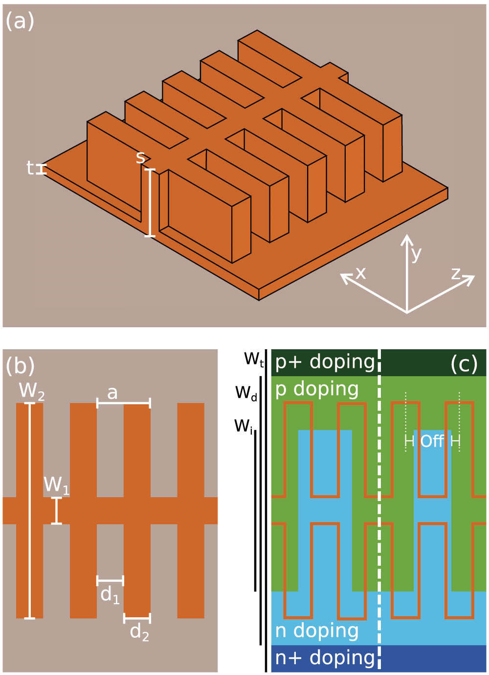
We analyze the grating waveguide structure shown in Fig. 1(a). The whole silicon structure is embedded in silica; further, the two materials are taken as lossless and nondispersive with dielectric constants and 2.093, respectively. The effect of dispersion on the group index is over a bandwidth of 50 nm. The silicon wafer thickness is , as in the platform of Ref. [46], and trenches are etched to a depth of 260 nm, leaving an unetched silicon thickness , to define the waveguide. The corrugation of the waveguide is defined by the widths of the thin and thick silicon trenches [see Fig. 1(b)], which are and , respectively. The period is , and the lengths . These parameters fix the lowest band edge at a wavelength while maximizing the slow-light bandwidth [19]. Adjusting the period by to account for a lithography resolution of 5 nm may result in a band-edge shift of .
Figure 1.Schematic of the slow-light waveguide with definition of the structure (a) in 3D and (b) in top view with grating parameters and (c) doping profiles. The silicon material in (a) and (b) (orange) is fully embedded in (gray). In panel (c), the boundary between p and n regions, which is perpendicular to the waveguide axis, can be either placed at the center of the wide grating section (left part) or displaced along the waveguide direction by the parameter Off (right part).
The doping scheme is shown in Fig. 1(c); it consists of lightly doped regions (n,p) as well as highly doped regions (n+,p+) defining the widths and , respectively. The p-n junctions are interleaved with a periodicity, , which is twice the periodicity of the optical waveguide. While in the main part of this work, we consider a transverse p-n junction boundary, which is aligned with the center of the wide grating sections [left part of Fig. 1(c)], we may also introduce an offset Off between the p-n junction boundary and the center of the wide sections [right part of Fig. 1(c)]. The depth of the interleaved trenches, or modulation width, is called in Fig. 1(c) and is the crucial parameter that controls the overlap between the travelling optical wave and the depletion regions. Note that, for , the doping pattern reduces to a lateral p-n junction, i.e., the p-n boundary is a straight line at the center of the optical waveguide.
We calculate the carrier densities in the junction by employing the Lumerical DEVICE software, which implements a finite-element solution of drift-diffusion equations. These simulations yield also the capacitance , the resistance , and the cutoff frequency , which is relevant for the dynamic behavior. Once the carrier densities at different values of the applied voltage are obtained, the change of the index of refraction (real part and imaginary part ) is calculated by well-known formulas of the plasma dispersion effect [6,8]: where , are the electrons and holes densities in , and is the wavelength in meters. The optical calculation is then performed using the aperiodic Fourier modal method [50], which yields the wavevector (real and imaginary parts) as a function of frequency . Calculating one period of the structure at any voltage yields the photonic dispersion . Its real part is used to calculate the variation of the phase shift with the voltage, , where is the wavevector variation, and is the phase shifter length. The imaginary part of the dispersion yields the propagation loss . Details are given in Ref. [45].
We now discuss the design strategy and the parameters adopted in this work. The heavy doping levels are fixed at , and the two outer widths are taken as and , respectively. The main free parameters of the p-n junction are the modulation width , the doping levels and in the lightly doped regions, and the offset Off. In silicon modulators, the n-doping concentration is often chosen to be higher than the p-doping concentration , in order to obtain similar plasma-dispersion contributions of electrons and holes in Eq. (1a). This produces an asymmetric depletion region, which is best compensated by introducing an offset in the junction position. With the present geometry of an interleaved p-n junction, our simulations have shown that, for , the behavior becomes sensitive to the offset parameter, and that, for increasing voltage, the depletion region tends to leak into the narrow sections of the grating, thereby compromising the overlap between the electric field and the depletion regions. Moreover, because the hole mobility in silicon is about three times smaller than the electron mobility, for the p-doped sections result in a much higher access resistivity, with a tendency to reduce the cutoff frequency. For these reasons, we decided to assume equal n- and p-dopings and, consequently, also a zero offset parameter. Our simulations indicated that the optimal values are . The modulation width has then been chosen with the requirement that the calculated cutoff frequency be higher than 12.5 GHz: this allows the modulator to transmit with a bit rate up to 25 Gbps using a nonreturn to zero format or up to 50 Gbps with PAM-4 encoding [51]. The calculations indicate that the maximum modulation width yielding is . These are the design values that we assume in this work in order to evaluate the modulator performance. An analysis of the behavior as a function of doping levels, modulation width, and offset, i.e., a tolerance analysis, is presented in Appendix A.
For completeness, Fig. 2 shows the group index and the propagation loss due to free carriers in the proximity of the band edge , at zero bias. Both quantities increase toward the band edge, due to the slow-light behavior. Their ratio is nearly constant and can be usefully expressed by the loss per unit time [25], which is in the considered spectral range. The results of Fig. 2 lead to a nearly wavelength-independent insertion loss, as we show in the next section.
Figure 2.Group index (left scale) and propagation loss per unit length at zero bias (right scale) as a function of wavelength. Parameters: see discussion in Section 2, in particular , , .
The use of an interleaved p-n junction is known to yield higher capacitance compared with lateral p-n junction geometry; thus, it is important to choose the parameters in order to achieve a reasonable modulation speed. The dynamic behavior of the modulator can be quantified by the cutoff frequency , which is independent of the length , since the capacitance and the resistance . Calculations are done using Lumerical DEVICE module by means of small-signal analysis, which yields the complex impedance .
In Fig. 3, we show the capacitance per unit length, the resistance time length, and the cutoff frequency. The capacitance decreases with applied reverse voltage, while the resistance increases. The first effect dominates and makes the cutoff frequency increase with voltage. For any reverse bias , the cutoff frequency is larger than 12.5 GHz, as we anticipated. Thus, the present structure parameters are sufficient to ensure high-speed modulation. A deeper analysis is reported in Appendix A.
Figure 3.(a) Capacitance per unit length (left scale) and resistance times length (right scale). (b) 3 dB cutoff frequency as a function of reverse voltage. Parameters: see discussion in Section 2, in particular , , .
When dealing with a single phase-shifter, two main performance metrics have to be considered: the modulation efficiency and the loss. is defined as the product between the applied voltage and the length needed to have a phase difference of between the biased and unbiased waveguide. Having a low is important because it allows using short phase-shifters and/or low driving voltages. Typical reported values for common modulators are [1,5], which reduce to when an interleaved p-n junction is used [34]. As for the loss, we take the figure of merit known as the insertion loss IL, where is the propagation loss per unit length evaluated at , while depends on the voltage. The insertion loss IL() represents the total loss of an optical signal for a length . A modulator will usually have a length ; thus, the actual insertion loss is reduced accordingly. Reported insertion losses are typically higher than 1 dB [5].
In conventional rib-based phase-shifters, these quantities depend on the p-n junction parameters and on the applied voltage, but they are almost independent of wavelength. However, this is no more the case for a slow-light structure, where both the phase shift and the propagation loss are proportional to the group index and thus increase when moving toward the band edge. This requires a more complex analysis of the results.
In Fig. 4, we show and IL() as a function of wavelength and voltage, for four different configurations: rib waveguide, lateral p-n junction; slow-light waveguide, lateral p-n junction; rib waveguide, interleaved p-n junction; slow-light waveguide, interleaved p-n junction. The rib waveguide is obtained by taking equal grating widths (instead of , for the slow-light waveguide); the lateral p-n junction is obtained by taking a modulation amplitude (instead of for the interleaved junction). Note that the values reported in Figs. 4(c) and 4(g) for the rib waveguide with interleaved p-n junction are close to those calculated in the literature [34]. The results and the comparison of the different structures highlight several important points.
is nearly wavelength-independent for the rib waveguides, while it depends on wavelength for the slow-light waveguides, where it goes to zero at the band edge . This is because is inversely proportional to the group index.
IL() is nearly independent of wavelength for all structures. In the case of the slow-light waveguide, this is because the increase of with the group index (see Fig. 2) is compensated by a corresponding decrease of .
For all structures, increases with voltage, while IL() decreases with voltage. The first effect follows from the fact that the width of the depletion region increases sublinearly with and so does at fixed length . The second effect basically reflects the decrease of with voltage.
The slow-light waveguide with interleaved p-n junction has better modulation efficiency and lower insertion losses compared with all other structures, at any wavelength and voltage. In the considered spectral range, is for ( for ) and IL for (2 dB for ). The free-carrier-induced loss of a phase shifter of length is as low as 0.61 dB for (0.3 dB for ). These values are strongly improved as compared with common modulators.
Considering Figs. 4(c) and 4(d), which refer to the interleaved p-n junction, the slow-light waveguide has better modulation efficiency compared with the rib waveguide over the whole spectral range considered.
On the contrary, if we consider Figs. 4(a) and 4(b), which refer to the lateral p-n junction, the slow-light waveguide improves upon the rib waveguide only in a limited wavelength region close to the band edge.
Figure 4.(Upper panels) , (lower panels) IL() for phase shifters in four different configurations (see text).
Results (5 and 6 shown above) are especially interesting and can be understood as follows. The variation of the phase shift with voltage can be expressed as In this equation, describes the slowdown of light (see Fig. 2) and is responsible for the decrease of toward the band edge in Figs. 4(b) and 4(d). The factor describes the effect of voltage on the optical behavior and can be written using electromagnetic perturbation theory as follows [52]: where . Thus, the frequency variation depends on the overlap integral between the intensity distribution of the travelling wave and the spatial variation of the refractive index due to the applied voltage. It is this factor that changes considerably for the four configurations that are compared in Fig. 4. Specifically, in the case of the lateral p-n junction, the slow-light waveguide has a smaller overlap integral than the rib waveguide because the electric field is mainly concentrated in the wide grating sections (), which are more extended than the rib waveguide itself (). For the case of the interleaved p-n junction, instead, the slow-light waveguide has a larger overlap integral than the rib waveguide, as the variation of the depletion region is optimally extended in the wide grating sections where the electric field is concentrated.
To illustrate this point, in Fig. 5 we show the charge density of the slow-light waveguide with the interleaved p-n junction [Figs. 5(a) and 5(b)] and the variation in charge density when changing the voltage from 0 to 1 V reverse bias [Fig. 5(c)]. The variation in charge density is close to the center of the wide grating section and corresponds to the maximum intensity of the electric field [Fig. 5(d)]. The overlap between the two maximizes the integral in Eq. (3). We emphasize that this effect is largely wavelength-independent, as the electric field of the lowest photonic band is concentrated in regions with high dielectric constant, thereby explaining why the slow-light waveguide with an interleaved p-n junction improves over the rib waveguide in the whole spectral range.
Figure 5.(a), (b) Charge densities for or , respectively. (c) Difference in charge density from 0 to 1 V. (d) Electric field (modulus) at . The values are taken at a height of 155 nm from the bottom of the waveguide and span one period along the propagation direction .
C. Mach–Zehnder Modulator Performance and OMA Analysis
The scheme of the modulator is shown in Fig. 6(a). It consists of a balanced Mach–Zehnder interferometer whose arms contain slow-light waveguide gratings acting as phase-shifters and providing a phase change . Each arm should also contain tapers to connect the slow-light waveguide to the surrounding conventional rib as well as additional phase-shifters (usually thermal or injection-based), which provide a static phase shift , so that the total phase shift is . However, because the taper and the additional phase shifter can be designed independently of the active part of the modulator, they will not be treated in the present paper. In the simplest case of equal propagation losses in the two arms, the two output powers can be derived as [9] where is the input power, , reduced by the propagation loss.
Figure 6.(a) Schematic structure of a Mach–Zehnder interferometer and (b) output power as a function of the phase difference between the arms (with definition of the quadrature working point): solid, , dashed, .
The working point of the modulator is chosen to be the quadrature point (), thus resulting in equal powers at the two outputs of the Mach–Zehnder modulator. The modulator is then operated in a push–pull configuration, meaning that the bias is alternatively applied to either one of the arms, in turn providing a modulation phase shift and changing the power balance between the outputs. This way, the signal power is modulated between the values and . The extinction ratio (ER) and the optical modulation amplitude (OMA) are then defined as and , respectively.
As can be seen in Fig. 6(b), both and power levels can be obtained with only one simulation, thanks to the symmetry of the working point. In the weak modulation limit and for equal losses in the two arms, the OMA is calculated as which shows that the OMA is increased when the modulation efficiency is improved and the losses are reduced. We shall focus on the OMA as a figure of merit, as it directly gives the strength of the signal at the output of the modulator, combining the two effects of modulation efficiency and losses [9,53]. In the following, we shall present results for the normalized OMA, given by and expressed in dB. Note that the inclusion of other sources of losses is straightforward because any additional loss (expressed in dB) just reduces the normalized OMA by the same amount.
To calculate the transmission spectrum of the modulator in the general case, we adopt the scattering matrix formalism outlined in Ref. [19]. We report in Fig. 7(a) an example of the calculated spectrum for a 0.5 mm long MZ modulator, operating at 1 V. The effect of slow light is clearly evident in the increased splitting between the and signals toward the band edge; then, the two curves cross when the group index continues to grow. The extinction ratio ER and the overall loss are reported in Fig. 7(b) and depend strongly on the wavelength.
Figure 7.(a) Transmission spectrum and (b) extinction ratio and total loss of an MZ modulator with length 0.5 mm and bias 1 V.
In Fig. 8, we show the normalized OMA as a function of wavelength, for different modulator lengths and voltages. The OMA curves are wavelength-dependent and bell-shaped (unlike in rib waveguides, where they do not depend on wavelength). The decrease of the OMA toward the band edge follows from the increase of the group index, which produces a growing modulation and a crossing of the , curves, and from the increase of the losses, both effects being visible in Fig. 7. For increasing wavelength far from the band edge, the increase of [see Fig. 4(d)] reduces the modulation amplitude and therefore the OMA.
Figure 8.Normalized OMA as a function of wavelength for different modulator lengths and applied voltages.
We are now in position to define the optical bandwidth of the modulator as the wavelength window in which the OMA is greater than a specified level. The target value sets the requirements on the quality of the output signal and can be chosen to suit a particular application at the design stage. Clearly, the bandwidth is not an issue in rib-waveguide modulators, where the OMA is wavelength-independent, but it becomes a crucial parameter in the case of slow-light modulators. For a given modulator length and voltage, we then calculate curves like those of Fig. 8, fix the required bandwidth, and determine the corresponding minimum OMA level. The results are shown in Fig. 9 for both slow-light modulators (, ) and rib-waveguide modulators (), both with interleaved p-n junction (notice the change in -scale from upper to lower panels). In the case of rib-waveguide modulators, the OMA level is independent of bandwidth, as expected, and the curves are similar to those of the literature [9], with a peak at a modulator length between 1 and 2 mm, depending on the voltage. For the slow-light modulator instead, the minimum OMA level depends on the specified bandwidth and increases on reducing the bandwidth. It is important to note that the OMA level is much higher for the slow-light modulator and that it peaks at smaller modulator lengths compared with the rib-waveguide modulator.
Figure 9.Minimum normalized OMA level as a function of modulator length, for different bandwidths (bw) and applied voltages. Upper panels: slow-light waveguide with interleaved p-n junction. Lower panels: rib waveguide with interleaved p-n junction, notice that the three curves with , 20, 30 nm are coincident. The upper scale of the axis represents the dissipated energy per bit, calculated as , where the capacitance is proportional to the modulator length.
In Fig. 9, we also report the dissipated energy per bit in the upper -scale. Indeed, the energy per bit is given by where the capacitance is proportional to the modulator length and is taken at the voltage to average over a voltage sweep. Thus, by calculating the junction capacitance per unit length (as reported in Fig. 3 for the slow-light waveguide and similarly obtained for the rib waveguide), we can express on the same scale of the modulator length. We see from Fig. 9 that, for the same OMA level, the slow-light modulator can operate with much lower energy dissipation than the rib-based modulator. The advantage of the slow-light modulator is especially evident at low voltage . For example, accepting an OMA level of , we can employ a modulator length of 0.3 mm (0.5 mm) with a bandwidth of (), and the corresponding values for are 0.22 pJ (0.4 pJ). Both the modulator length and the dissipated energy are much smaller than in conventional modulators. Having a shorter modulator length has the additional advantage that it can allow treating the entire phase shifter as a lumped element, without the need for multistage or travelling-wave electrodes, thus greatly simplifying the driving electronics. Moreover, it makes the modulator more tolerant with respect to fabrication-induced losses.
The main message from the above results can be summarized as follows: while the slow-light bandwidth is limited by the group-index curve (see Fig. 2), the advantage of the slow-light modulator with interleaved p-n junction extends over an optical bandwidth that is much larger than the slow-light bandwidth. This traces back to the role of the overlap integral in Eq. (3) in addition to the slowdown factor. Comparison with the rib waveguide clearly highlights the advantage of the present slow-light modulator in terms of length, OMA level, and energy consumption.
The optical bandwidth as defined above incorporates performance requirements on modulator efficiency and loss. In a given application, the optical bandwidth has to be specified in relation with the overall system requirements. For example, modulation architectures based on four-lane WDM for intra-data center communication may have four different wavelengths in the O-band that are spaced by 8 nm, resulting in a bandwidth requirement of . This is quite compatible with the above design of a 0.5 mm long modulator having in the whole optical bandwidth. Much looser bandwidth requirements arise with a channel spacing of 800 GHz or lower. Note that, in all cases, the useful bandwidth starts a few nm away from the band edge (see Fig. 8). This helps mitigate effects due to group index dispersion, or effects arising from fluctuations in modulator uniformity that may shift or smear out the band edge to some extent. Here again, there is a strong advantage in combining the slow-light waveguide with an interleaved p-n junction, as this allows extending the useful bandwidth far away from the band edge and much beyond the slow-light bandwidth.
It is important to discuss the sensitivity of the results with respect to disorder-induced losses that arise from fabrication imperfections. While such losses have been thoroughly investigated in PhC waveguides, there are few reports on disorder-induced losses in slow-light grating waveguides. Because the losses increase toward the band edge following the increase of the group index, they are better expressed in terms of a loss per unit time [25]. The measurements on a slow-light modulator reported in Ref. [11] (Fig. 5) indicate that the losses are of the order of 200 dB/ns. This value includes the free-carrier loss in addition to disorder-induced loss. Systematic analysis of slow-light waveguide gratings in Ref. [54] (Fig. 11) leads to disorder-induced losses of the order of 100–120 dB/ns over a wide spectral range. These values should be compared with free-carrier loss in our structure, which is (see Fig. 2). To evaluate the effect of disorder-induced loss, Fig. 10 shows the OMA as a function of wavelength for a 0.5 mm long modulator, and the minimum OMA level as a function of modulator length for 10 nm bandwidth, for 1 V reverse bias and increasing values of the disorder-induced loss. The OMA values are obviously reduced by the additional loss, by an amount that ranges from to . Importantly, the OMA curves are not distorted; therefore, the optical bandwidth is not changed by the additional loss. We note that the minimum OMA level in Fig. 10(b) is still improved compared with the rib waveguide with the interleaved p-n junction shown in Fig. 9(e). The rapid progress in photonic nanofabrication technologies, especially the recent advances in immersion lithography [55,56], suggests that disorder-induced losses may yield a penalty of no more than in the OMA signal, while maintaining the advantages of short modulator length and low energy dissipation.
Figure 10.(a) Normalized OMA as a function of wavelength for an modulator. (b) Minimum normalized OMA level as a function of modulator length for 10 nm bandwidth, for different values of the additional disorder-induced loss. The upper scale in (b) represents the dissipated energy per bit, as in Fig. 9. The reverse applied voltage is .
Figure 11.Various figures of merit: capacitance per unit length, resistance times length, 3 dB cutoff frequency, and IL at . The quantities are plotted as a function of doping level at fixed modulation width and offset (left panels), as a function of modulation width at fixed doping and offset (central panels), as a function of offset at fixed doping and modulation width (right panels). Green lines and symbols: . Black lines and symbols: . Red lines and symbols: . Blue lines and symbols: .
We have shown that proper design of an interleaved p-n junction can greatly enhance the performance of slow-light modulators. Starting from parameters that are compatible with high-speed modulation, the figures of merit (modulation efficiency) and IL() (insertion loss for length) are improved over phase-shifters based on rib waveguides or on slow light with a lateral p-n junction. This is due to a combination of two effects: (1) the slowdown of light toward the band edge, and (2) the increased spatial overlap between the travelling electromagnetic wave and the variation of the depletion region under bias.
We have developed a full simulation of Mach–Zehnder modulators with the present slow-light design, focusing on the OMA as a key figure of merit that accounts for modulation efficiency and losses. By defining the optical bandwidth as the spectral window with an OMA greater than the target level, the advantage of the slow-light modulator with interleaved p-n junction extends over an optical bandwidth that can be much larger than the slow-light bandwidth. At 1 V reverse bias, modulator lengths below 0.5 mm and energy consumption below 0.5 pJ/bit can be obtained with bandwidths of several tens of nm.
Fabrication of such modulators implies requirements on gap size ( with the present design) that are within the capabilities of current Si-photonics platforms. The short modulator length makes the structures relatively tolerant against fabrication-related losses and promising for a major reduction of energy dissipation in the device.
Acknowledgment
Acknowledgment. The authors acknowledge useful discussions with C. Baudot, F. Boeuf, A. Fincato, F. Gardes, C. Lacava, R. Sheehan, F. Svelto, and E. Temporiti.
APPENDIX A: TOLERANCE ANALYSIS
We start from the basic structure described in Section 2 and vary, in turn, the parameters (light doping levels, taken to be equal), (modulation width), and Off (offset between junction position and center of wide grating sections). This allows us to justify the design parameters used in this work and to discuss the sensitivity with respect to each of these parameters. The results are summarized in Fig. 11 for five quantities: the capacitance per unit length; the resistance times length; the 3 dB cutoff frequency; the modulation efficiency ; and the insertion loss IL(). The last two quantities are evaluated at the wavelength : the insertion loss is nearly independent of wavelength, while the wavelength-dependence of is similar to Fig. 4(d) of the main text.
Dependence on Doping Levels
In the left panels of Fig. 11, we show the results as a function of doping levels in the lightly doped regions, keeping a fixed modulation width and offset . The capacitance increases with doping, while the resistance decreases. As a result, the cutoff frequency is weakly dependent on doping. The modulation efficiency improves on increasing the doping, but the improvement is rather limited for . On the other hand, the insertion loss increases with the doping. In this work, we choose the doping levels as a satisfactory trade-off that yields a good modulation efficiency, while avoiding an excessive increase of the capacitance and of the losses.
Dependence on Modulation Width
In the central panels of Fig. 11, we show the results as a function of modulation width, keeping fixed doping levels and zero offset. Both the capacitance and the resistance decrease with decreasing ; thus, the cutoff frequency increases rapidly with decreasing and is maximum for , i.e., for the lateral p-n junction. Choosing ensures a cutoff frequency that is larger than 12.5 GHz for any driving voltage . On the contrary, the modulation efficiency improves, and the insertion loss decreases on increasing the modulation width. However, we notice that the values of for are close to those for , and the same happens for the insertion loss. Thus, the value for the modulation width represents the best trade-off between the competing requirements of having a reasonably high cutoff frequency while optimizing the modulation efficiency.
The reason why the modulator performance for is close to that for is that yields a good overlap between the field distribution and the change of the depletion region (see Fig. 5). Increasing the modulation width beyond this value does not appreciably improve , while it unnecessarily increases the capacitance.
Dependence on Offset
In the right panels of Fig. 11, we show the results as a function of the offset parameter Off, keeping fixed doping levels and modulation width . The dependence of , , and on the offset parameter is relatively weak and the cutoff frequency is always for any voltage . The optimal value for both the modulation efficiency and the insertion loss IL() is close to zero offset, and the tolerance is around 20 nm. We remark that both properties hold only when the electron and hole doping levels are chosen to be equal, as discussed in Section 2.
[13] A. Zanzi, A. Rosa, A. Oriol, P. Sanchis, J. Marti, A. Brimont. Advanced high speed slow-light silicon modulators in the O-band for low power optical interconnects in data centers. 14th International Conference on Group IV Photonics, 149-150(2017).
[14] R. Hosseini, A. Khachaturian, M. Cătuneanu, P. P. Khial, R. Fatemi, A. Hajimiri, K. Jamshidi. Compact, high extinction ratio silicon Mach-Zehnder modulator with corrugated waveguides. Conference on Lasers and Electro-Optics, SM3B.6(2018).
Marco Passoni, Dario Gerace, Liam O’Faolain, Lucio Claudio Andreani. Optimizing an interleaved p-n junction to reduce energy dissipation in silicon slow-light modulators[J]. Photonics Research, 2020, 8(4): 457