1Wuhan National Laboratory for Optoelectronics, School of Optical and Electronic Information, Huazhong University of Science and Technology (HUST), Wuhan 430074, China
2State Key Laboratory of Advanced Optical Communication Systems and Networks, Department of Electronic Engineering, Shanghai Jiao Tong University, Shanghai 200240, China
3State Key Laboratory of High Performance Complex Manufacturing, Central South University, Changsha 410083, China
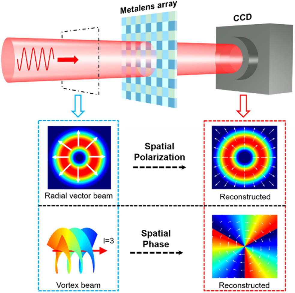
The real-time measurement of the polarization and phase information of light is very important and desirable in optics. Metasurfaces can be used to achieve flexible wavefront control and can therefore be used to replace traditional optical elements to produce a highly integrated and extremely compact optical system. Here, we propose an efficient and compact optical multiparameter detection system based on a Hartmann–Shack array with subarray metalenses. This system not only enables the efficient and accurate measurement of the spatial polarization profiles of optical beams via the inspection of foci amplitudes, but also measures the phase and phase-gradient profiles by analyzing foci displacements. In this work, details of the design of the elliptical silicon pillars for the metalens are described, and we achieve a high average focusing efficiency of 48% and a high spatial resolution. The performance of the system is validated by the experimental measurement of 22 scalar polarized beams, an azimuthally polarized beam, a radially polarized beam, and a vortex beam. The experimental results are in good agreement with theoretical predictions.
1. INTRODUCTION
The amplitude, phase, and state of polarization (SOP) are fundamental parameters for describing light waves. At present, however, most photodetectors are only sensitive to the light intensity, which makes traditional polarization and phase detection systems complex, bulky, and difficult to integrate. Metasurfaces are ultrathin two-dimensional metamaterials with subwavelength features that can flexibly manipulate the amplitude, phase, and SOP of the light. Over the last few years, metasurfaces have become a versatile platform for wavefront control. Metasurfaces have subwavelength thicknesses, which has been exploited to develop compact optical devices with metasurfaces, such as polarization elements [1–8], holograms [9–11], and metalenses [12–19]. Compared with traditional lenses, metalenses offer the advantages of higher compactness and no spherical aberrations. Therefore, research on metalenses is becoming one of the most popular directions in the field of metasurface-based optics. Numerous studies have been conducted on plasmonic metasurfaces [20–23]. These studies are fundamentally limited in terms of the efficiency of utilizing visible and NIR wavelengths for transmission operation, which poses a key obstacle to the practical application of metasurfaces. These problems can be solved by using dielectric metasurfaces [24–29]. Therefore, many novel metalenses based on dielectric metasurfaces have been reported recently, including dielectric polarization-dependent metalenses [30–34], dielectric polarization-independent metalenses [35–37], and broadband achromatic dielectric metalenses [38–40]. The fabrication of these planar lenses is straightforward, and the lenses can be vertically integrated and can potentially replace or complement their conventional refractive and diffractive counterparts, facilitating further miniaturization of high-performance optical devices and systems.
In a previous work, we demonstrated a dielectric metalens array for multiparameter detection operating at 1550 nm [41]. The unit elements of the metalenses are composed of elliptical silicon pillars. Each pixel of the array consists of six different metalenses that can converge differently polarized light onto the focal plane. The phase gradient and the SOP of the incident beam can be measured by detecting the positions and intensities of the focal points.
Here, we continue this research and propose and experimentally verify a new type of metalens array operating at 1550 nm. Each pixel of the silicon-based metalens array consists of a submetalens array that replaces the previous submetalens array. This configuration affords a 1.5-fold theoretical improvement in the spatial resolution, which is beneficial for applications in optical imaging and optical detection. In addition, by redesigning the unit cell of each metalens (i.e., by reducing the lattice constant from 1.5 to 1.0 μm and optimizing the unit element size for higher transmittance), we significantly improve the average focusing efficiency from 28% to 48%. In the experiments, we first accurately characterize the SOP of 22 different incident-polarized beams by one pixel of the array. The average relative error between the theoretical results and experimental results is as small as 4.24%. Next, we detect two common light beams with nonconstant SOPs (a radially polarized beam and an azimuthally polarized beam) and a vortex light beam with a spiral wavefront, demonstrating that our design is also applicable to beams with complex SOPs and wavefronts. The experimental results are in good agreement with the theoretical values.
Sign up for Photonics Research TOC. Get the latest issue of Photonics Research delivered right to you!Sign up now
2. PRINCIPLE AND DESIGN
Figure 1.Schematic shows the dielectric metalens-based Hartmann–Shack array for a high-efficiency optical multiparameter detection system. The system can simultaneously measure the spatial polarization and phase profiles of optical beams. The colors are only used to enhance the clarity of the image and to distinguish metalenses with different polarization sensitivities in the array.
Figure 2.Schematic and design of metalenses. (a) Scheme for one pixel of a metalens array. (The colors indicate different polarizations.) The dotted crosses on the focal plane correspond to the centers of particular metalenses. (b) Scheme for one unit element of a metalens; (c), (d) simulation results for intensity transmittance and phase shifts of unit elements under normal incidence of -polarized light. The white triangles indicate the transmittance, phase, and dimensions of 11 elliptical silicon pillars along the -positive axis from the center of a -polarized metalens. The white circle at () highlights the structural parameters used for an -polarized sensitive metalens.
As shown in Fig. 2(b), the unit element of the metalens is an elliptical silicon pillar that is placed on a layer of silica with a constant height and a square lattice constant . The primary function of the pillar is to locally shift the phase of the incident light. The wavefront of the transmitted beam can be flexibly manipulated by adjusting the spatial scales of the geometrical parameters (the major axis , the minor axis , and the orientation angle ). The finite-difference time-domain (FDTD) method (Lumerical Inc. FDTD Solutions) is applied to calculate and analyze the characteristics of the unit element to manipulate the amplitude and phase of the incident beam. Figures 2(c) and 2(d) show the intensity transmittance and the phase shifts of the unit element for different dimensions when the -polarized light is incident normally. These data are combined with the following methods to obtain a blueprint for one pixel of the metalens array. To design a flat focusing lens for a prescribed light polarization, the phase shift of the respective polarized component that is introduced by each elliptical silicon pillar in the plane must satisfy Eq. (1) [14], where denotes the focal length of the lens, denotes the working wavelength, and denotes the phase that is needed at the () location of each elliptical silicon pillar in the plane. The constant denotes the phase of the elliptical silicon pillar at the center, which is just a reference phase and is set to 0 here. In this study, the focal length and the working wavelength are positioned at 30 μm and 1550 nm, respectively.
The design of the metalens array consists of two components—a linearly polarized sensitive metalens and a circularly polarized sensitive metalens, which are based on propagation phase theory and Pancharatnam–Barry (PB) phase theory [42–44]. The dimensions of all the selected elliptical silicon pillars for the metalenses are based on the following three conditions. (1) The dimensions ( and ) of all the selected elliptical silicon pillars should be polarization-dependent. (2) The local phase of all the selected elliptical silicon pillars should satisfy phase Eq. (1). (3) Once conditions (1) and (2) are satisfied, elliptical silicon pillars with high transmittance are selected as much as possible. The design of a linearly polarized sensitive metalens depends mainly on propagation phase theory. Phase coverage over the range can be achieved by changing the dimensions of the unit element. Taking the -polarized sensitive metalens as a theoretical design example, the structural data points with the higher intensity transmittance in Fig. 2(c) are selected as much as possible, while ensuring that each selected elliptical silicon pillar satisfies the above-mentioned conditions (1) and (2). To provide more details on the design of the elliptical silicon pillars, the 11 elliptical silicon pillars along the -positive axis from the center of the metalens are demarcated in Figs. 2(c) and 2(d). Although the transmittance of several elliptical silicon pillars is not high, this is the highest transmittance that can be obtained while meeting the polarization dependence and local phase requirements. Our goal is to choose as many elliptical silicon pillars with as high transmittance as possible that can satisfy the first two conditions. Then, -polarized and -polarized metalenses are realized by performing 90 deg and rotations of these silicon pillars, respectively.
In addition, the PB phase shift is adopted to design a metalens for circularly polarized light. All the unit elements have the same dimensions with and , which is demarcated by the white circle in Figs. 2(c) and 2(d), and phase variation is achieved via the rotation of these unit elements. Equation (2) is derived from the Jones matrix calculus, and it describes the complex amplitudes of the transmitted light for -polarized incident light [15],
Here, and denote the complex transmission coefficients of the linearly polarized incident beam along the major and minor axes of the elliptical silicon pillars, and denotes the orientation angle in the counterclockwise direction. The additional phase shift increases linearly from 0 to as varies from 0 to . The transmittance is improved by making the first group of terms (which have the same handedness as the incident light) vanish by choosing the smallest absolute value of and maximizing the second group of terms (which have the opposite handedness to the incident light) by choosing the largest absolute value of [see the white circle at (800 nm, 224 nm) in Figs. 2(c) and 2(d)]. Compared with the previous consideration of only making the first terms vanish, the total transmittance has been improved. Under this condition, the incident light is almost completely converted into the opposite circular-handedness that can be manipulated by the PB phase shift, which improves the efficiency of the circular polarization conversion. More importantly, this procedure increases the transmittance of each elliptical silicon pillar and maximizes the efficiency of the corresponding circularly polarized incident light. The additional phase shift spans the range by varying the rotation angle of the elliptical silicon pillars, and the transmittance of each elliptical silicon pillar is greater than 0.7. All the unit elements of the metalens for the -polarized components are obtained in this manner.
Figure 3.Scanning electron micrographs and intensity distributions of a manufactured metalens array. (a) Local scanning electron micrograph of a fabricated metalens array. The white rectangle indicates one pixel of the array. (b) Corresponding magnified scanning electron micrograph of one pixel, where the polarization bases are denoted by letters for each metalens; (c)–(d) oblique view of the selected parts of the metalenses; (e)–(f) intensity profiles along the axis, passing through the focus, together with a Gaussian fit for the -polarized sensitive metalens and -polarized sensitive metalens; the diameter of the focal spot is 7 μm.
The focusing efficiency is defined as the ratio of the light power of the focal spot to the power collected by the camera on a metalens; this value is 41% for a linearly polarized metalens and 55% for a circularly polarized metalens, and different from the theoretical predictions of 69% and 72%. The deviation between the experimental results and theoretical predictions can be attributed to fabrication errors and imperfections in the optical components. To eliminate the deviation, on the one hand, it is possible to optimize the structure with high dimensional tolerance; on the other hand, the structural dimensions can be calibrated and corrected by scanning electron microscopy during the manufacturing process to ensure that they are as close to the theoretical values as possible. The improvement in the focusing efficiency can be explained by the following two considerations. The first consideration is that the reduction in the lattice constant from 1.5 μm to 1.0 μm increases the density of the elliptical silicon pillars in a metalens of the same size. Increasing the number of elliptical silicon pillars smooths out the phase gradient across the metalens: more elliptical silicon pillars participate in the manipulation of the incident beam to form the phase required for focusing, which helps to improve the focusing efficiency. Note, however, that although the focusing efficiency of the metalens can be improved by decreasing the lattice constant to increase the number of elliptical silicon pillars, the lattice constant cannot be reduced infinitely. A reduction in the lattice constant inevitably leads to a reduction in the dimensions of the elliptical silicon pillars, which increases the difficulty of the manufacturing process to a certain extent. Therefore, taking both of the above-mentioned considerations into account, we select a lattice constant of 1.0 μm instead of the original value of 1.5 μm. Second, we select dimensions for the unit elliptical silicon pillar so that the pillar has a higher transmittance to satisfy the local phase requirement and polarization dependence. The increased transmittance of the unit elliptical silicon pillar means that more incident light has been utilized, which also helps to improve the focusing efficiency.
Generally, the SOP can be determined from the Stokes parameters, which can be obtained by using Eq. (3) [45,46], where are the four components of the Stokes parameters. The intensities of the six polarization components refer to the intensities of the horizontal, vertical, deg, deg, left-circular, and right-circular polarization components of the incident beam, respectively. Note that the Stokes parameters that are described above are calculated based on the intensities of six polarization components, whereas only three types of linear polarization components and one circular polarization component are needed to reconstruct the Stokes parameters [33]. And then the Stokes parameters can be rewritten as Eq. (4). Moreover, the spatial resolution can be effectively improved by 1.5-fold with this method,
For locally linearly polarized light, the Stokes parameters can be characterized by the polarization angle ,
In addition, this detection system is similar to a Hartmann–Shack wavefront sensor [47,48] and can detect the phase gradients of an incident beam, which can be calculated by using Eqs. (6) and (7),
In the equations above, and denote the phase slopes of a wavefront in the and directions, and and denote the position shifts of the focus. The wavefront of the incident beam can be reconstructed by calculating and analyzing the focus shifts and phase gradients.
3. EXPERIMENTAL RESULTS
A. SOP Detection
Figure 4.Experimental validation of SOP detection with one pixel. (a) Optical setup for polarization detection. LP, linear polarization; , quarter-wave plate; , half-wave plate; VP, vector wave plate; L1, L2, lens; OL, objective lens; CCD, charge-coupled device. (b) Intensity distributions of the focal points in one pixel for incident horizontal or vertical linear polarization (“” and “”), diagonal linear polarization (“” and “”), and circular polarization (“” and “”); (c) experimentally reconstructed (stars) Stokes parameters (, , ) and theoretical predictions (small circles) are compared on a Poincaré sphere (see Data File 1).
Figure 5.Detection and reconstruction of two vector beams. (a), (b) Intensity distributions for two vector beams. The blue arrows denote the local SOPs. (c), (d) Raw data of measured focal points for two vector beams; (e), (f) reconstructed polarization profiles. The black arrows correspond to the measured local polarization vectors, and the red arrows correspond to the theoretical predictions. The dashed gray lines are drawn to identify individual pixels.
Figure 6.Detection and reconstruction of the vortex beam. (a) Schematic of the optical setup. L1, L2, L3, L4, lens; A, aperture; P, polarizer; SP, splitter prism; SLM, spatial light modulator; and OL, objective lens. (b) Intensity distribution for the vortex beam; (c) raw data of measured focal points for the vortex beam; (d) phase gradients (pink arrows denote theoretical results, and black arrows denote experimental results) and reconstructed wavefront (false-color scale) of the vortex beam. The dashed lines are drawn in above images to distinguish individual pixels of the metalens array. The length of the reference arrow is 0.4 rad/μm.
Note that although the above-mentioned experiments for polarization reconstruction and phase detection are carried out separately, the system can realize the measurements of polarization states and wavefront profiles simultaneously, which was confirmed in our last study and is also discussed in the wavefront measurement section of this study. Moreover, because the degree of polarization can be obtained by using the measured Stokes parameters, the system is also clearly suitable for partially polarized beams.
The metalens array proposed in this study has a higher spatial resolution and focusing efficiency than the previously developed structure. Compression of the subarray into a subarray results in a 50% increase in the spatial resolution. For linearly incident polarizations, we measured an average focusing efficiency of 41%, which is higher than the previous measurement of 30%. For circularly incident polarization, the focusing efficiency is increased to 55%, which is superior to the previous value of 26%. The increase in efficiency can be attributed to the following two considerations. The first consideration is that reducing the lattice constant from 1.5 μm to 1.0 μm increases the density of the silicon nanopillars in a metalens of the same size and smooths out the phase gradient across the metalens. A larger number of elliptical silicon pillars participate in the manipulation of the incident beam to form the phase required for focusing, which helps to improve the focusing efficiency. The second consideration is that the dimensions of the selected unit elliptical silicon pillar increase the transmittance by satisfying the focus phase requirement and polarization dependence. The increased transmittance of the unit elliptical silicon pillar means that more incident light is utilized, which also helps to improve the focusing efficiency. For a linearly polarized metalens, elliptical silicon pillars with high transmittance are selected as much as possible. For an -polarized metalens, we maximize the second group of terms in Eq. (2) by choosing the largest absolute value of , while selecting the smallest possible value for in the first group of terms. Under this condition, the incident light is almost completely converted into the opposite circular-handedness, and the transmittance of the unit elliptical silicon pillar is increased. It is well known that focusing efficiency and resolution are critical in optical imaging and optical probing. The increase in the focusing efficiency shows that more incident light is utilized, enabling weaker signals to be detected. The improvement in the resolution can further enrich the details of the incident light and increase the detection capability of the device. The improvement in the focusing efficiency and resolution helps to increase the accuracy of the measurement of the incident light and to increase the detection capability of the device. In the experiments, the average measurement error of the scalar polarized beams is 4.24%, which is smaller than our previously obtained value of 4.83%. For two vector-polarized beams (a radially polarized beam and an azimuthally polarized beam), the measurement errors are 6.28% and 2.49%, respectively, which are better than our previously obtained values of 6.33% and 4.46%. The measurement error in the vortex beam detection is 6.4%, and our previously obtained value was 8.0%.
In summary, in this study, we have demonstrated the operation of an optical multiparameter detection system based on an all-dielectric metalens array at 1550 nm. Each pixel of the metalens array consists of four differently polarized sensitive metalenses. By measuring the intensities and positions of the focal points, the system can realize the real-time detection of the SOP and wavefront distributions of the incident light.
Acknowledgment
Acknowledgment. We are grateful for device fabrication support from the Center of Micro-Fabrication and Characterization (CMFC) in the Wuhan National Laboratory for Optoelectronics (WNLO) of Huazhong University of Science and Technology (HUST).
[21] F. Monticone, N. M. Estakhri, A. Alu. Full control of nanoscale optical transmission with a composite metascreen. Phys. Rev. Lett., 110, 203903(2013).