Abstract
Metamaterial absorbers (MAs) serve as important electromagnetic wave-absorbing devices that have captured the attention of researchers for a long term. Functioning as sensitive detectors to determine perturbations in an ambient environment is another significant subsidiary function. Here, we theoretically propose an optimized fabrication method to implement terahertz MAs with fewer steps and also evaluate both absorption and sensing performances of such MAs realized by the new method. Simulation findings demonstrate that such MAs can basically maintain the original absorption features perfectly, including near-complete absorption at resonance as well as strong robustness to wide incident angles. Specifically, the full width at half-maximum and quality factor of the absorption resonances attenuate less than 26% and 8% with this new method, remaining in the ranges of and for two selected example MAs. More significantly, sensing capacities of this type of MA, in terms of maximum detection range (enhancing at least 9%), observable spectral modulation (increasing at least 6.3%), and refractive index sensitivity, are improved to a large extent because of more intense coupling between resonant field and matter in the case of surface-relief MAs. This stronger coupling results from exposing more spots of the resonantly high field to direct contact with an approaching analyte, which is illustrated by field profiles of the MAs at resonance in this work. Additionally, other desirable absorber features are also explored with such MAs, like functioning as building blocks to configure multiband MAs and strong robustness against fabrication errors. Such new-style terahertz MAs shown in the paper, acting as good examples, not only prove that terahertz MAs can be fabricated by the proposed time- and cost-saving route in contrast to the traditional MA fabrication process, but also can serve as novel platforms to explore other intriguing terahertz photonic effects, such as the field enhancement effect.1. INTRODUCTION
It has been well established that electromagnetic waves with specific energy levels can couple with matter at micro- or nanoscale, which has attracted extensive attention from the scientific community for many years [1–3]. These coupling mechanisms lead to occurrences of various and intriguing phenomena with enriching content in physics, like localized or propagating surface plasma resonance [4], extraordinary/enhanced optical transmission [5], and negative refraction [6]. Meanwhile, to meet multitudinous actual needs, a wide range of functional components based on different coupling processes have been proposed, both theoretically and experimentally [7–12]. Terahertz metamaterial absorbers (THz MAs) are put forward as one type of such components, which play roles of significant importance in perfect absorption [7,13], sensing [14,15], imaging [16], thermal emitters [17], and so on. Generally, MAs feature a sandwich-like configuration consisting mainly of a top-patterned metasurface layer, a dielectric supporting layer, and a metal ground layer. With such a Fabry–Perot (F–P) cavity design, an incident THz field is resonantly enhanced at given frequencies where the incident electromagnetic energy is trapped within the MA cavity. Accordingly, the spectral response for the MAs generally shows distinct resonance reflection dips that are sensitive to certain physical attributes of ambient environment, like refractive index (RI). This characteristic makes MAs well-performing metamaterial sensing systems to detect perturbations in the surrounding media [14].
Metamaterial sensing refers to a method of detecting alterations in surrounding media by observing resulting modulations of amplitude or frequency location of resonances in the frequency spectrum of metamaterials. A variety of metamaterial sensors, including thin-film metasurfaces [18,19], resonant MA cavities [14,20], and three-dimensional (3D) metamaterials [21], are proposed, and the sensing behaviors are evaluated with a well-known indicator, the figure of merit (FOM). In general, the higher the FOM is, the better performance metamaterial sensors demonstrate. The FOM of sensing performance is commonly expressed as ; refers to the quality factor of the concerned resonance and denotes the percentage frequency shift (FS) of the concerned resonance peak/dip induced by the change of surrounding media [21]. Following the line hinted at by the equation, we can start from two aspects to enhance the sensing capacity of metamaterial sensors. One is to design a metamaterial sensor with a higher resonance, while the other is to make the concerned resonance displace with a larger step for the same surrounding change. The first route has been extensively explored in the last few years, and plentiful methods have been shown to realize high- resonances [22–25]. On the other side, several methods aim at highlighting the influence of surrounding dielectric change by reducing the substrate effect, such as etching away parts of a high-index substrate [26–33] or using a low-index substrate [34,35] in order to achieve a larger spectral modulation with the same dielectric alteration.
In this paper, we theoretically optimize the traditional fabrication process for realizing THz MAs and analyze the feasibility compatible with the existing surface micromachining process. To illustrate our claim, two of the most common THz MA configurations are selected as objects of study, and the attributes of the new-style and original MAs are compared in terms of absorption and sensing capacities under numerical simulations. The findings confirm that, in contrast to MAs realized by the traditional process, absorption attributes of the new-style MAs are principally kept, and more importantly, sensing capacities of the new MAs are greatly improved due to the surface-relief (SR) design. Then we numerically calculate field profiles of the MAs to elucidate the underlying physical mechanism. Finally, we show that the absorption performance of these new-style MAs can be further improved by simple structural optimization and also explore other features of such MAs. The proposed fabrication method for THz MAs can be utilized to implement ultrasensitive MA detectors and other functional devices at the THz band.
Sign up for Photonics Research TOC. Get the latest issue of Photonics Research delivered right to you!Sign up now
2. PROPOSED FABRICATION PROCESS
Figure 1 demonstrates the proposed fabrication process for MAs step by step. Compared with the traditional MA fabrication process [36,37], this new method just simplifies the last few steps of the workflow. As indicated by the light gray parts in Fig. 1, bulk silicon (Si) wafers are chosen as MA substrates because of the high transmission characteristics at the THz band of interest. A 200-nm-thick aluminum (Al) film is deposited on Si substrates as a ground layer, which can be done by thermal or e-beam evaporation, as indicated by the purple parts. Then a dielectric layer, as shown by the green parts in Fig. 1, is coated on the metal film and patterned by employing a matched etching method or laser direct-writing technology [38–40]. As the last step, another 200-nm-thick Al film is deposited on the top surface of the whole structure. Here, it should be noted that the concomitant Al layer deposited on the Al ground film in the last step shown in Fig. 1(e) will inevitably change the final thickness of the Al ground layer; however, this will not exert an undesirable impact on the main features of MAs, like absorption. When the metal layer thickness is well beyond skin depth at the THz frequency of interest, the thickness becomes insignificant, which has been well established in the traditional THz absorber cases and also proved later by Fig. 10 and the accompanying discussion.
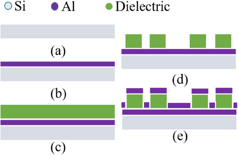
Figure 1.Schematic drawing shows the proposed process for fabricating an MA in detail. The processing steps are listed alphabetically. Different colors represent various materials, that is, light gray, purple, and green parts refer to the Si substrate, Al parts, and dielectric layer, respectively.
Following the above procedure, a novel type of SR-shaped MAs can be fabricated, and such MAs are realized with fewer steps than those of the traditional workflow. Still, it is worthwhile to stress that a key issue of selecting appropriate materials to serve as dielectric supporting layers needs to be addressed in the practical implementation process. The first choice can be from a group of photosensitive materials while taking into account other on-demand attributes, like rigidity and stability. Or the preferred material can be a relatively hard material compatible with laser direct-writing technology, e.g., polymer or Si. For different processing methods, materials with different physical and chemical properties can be selected according to practical needs.
3. PERFORMANCE COMPARISON
A. Selected MA Examples
To validate the feasibility and universality of the proposed fabrication method, we choose two of the most common MA designs as examples to explore the attributes of MAs fabricated by the new method, as shown in Fig. 2. The two typical MA designs are chosen since both of them are representative and fundamental MA configurations and also feature a wealth of advantageous characteristics, such as simple structure, polarization insensitivity, and wide incident angle tolerance. Figures 2(a) and 2(c) demonstrate two flat MAs realized by the traditional fabrication flow as control MAs, while Figs. 2(b) and 2(d), respectively, display SR cross-shaped (SRC) and SR square-shaped (SRS) MAs to be studied. For simplicity and distinguishability, in the rest of the paper, the MAs shown in Figs. 2(a) and 2(c) will be termed as cross MA and square MA, respectively. Likewise, the MAs in Figs. 2(b) and 2(d) are labeled as SRC MA and SRS MA. For all the numerical simulations throughout this paper, all the MAs are excited by the same THz source, i.e., an incident THz wave illuminates the MAs vertically from the top, and the electric component is parallel to the arms of the cross- or square-shaped parts along the axis, while the direction of the magnetic field is, along with the other perpendicular arms, along the axis. All the numerical calculations are conducted with a frequency solver based on the finite-integration method. In all the simulations, the boundary condition of unit cell is employed in both and directions to imitate MAs with an infinite array size. As we stated before, metal Al () is used to build subwavelength resonators and the ground layer in the models, whereas a Si () wafer is chosen as a substrate. Also, in our entire simulation, dielectric material with is used as the supporting layer.

Figure 2.3D schematic plot for the MA examples and the incident THz field polarizations. All the MAs are excited by the same incident field polarizations shown at the top right corner of the plot. Different colored parts represent different materials. (a) and (b) are the original and remolded (SR) cross-shaped MAs. (c) and (d) are the original and remolded (SR) square-shaped MAs. For all MAs, lattice constant, and thicknesses of metal and dielectric layers are labeled as , , and , while and represent length and width of the metallic stripes constituting the cross and square structures in MAs, respectively.
As shown in Figs. 2(a) and 2(b), the cross and SRC MAs share the same structural design except for differences in the coverage area of the dielectric layer. Their common geometric parameters used in simulations are lattice constant , Al thickness , dielectric thickness , arm length , and arm width . Similarly, the structures of the square and SRS MAs shown in Figs. 2(c) and 2(d) are also identical except for the rugged surface, and the geometric parameters jointly used in simulations are lattice constant , Al thickness , dielectric thickness , arm length , and arm width .
B. Absorption Performance Comparison
The absorption spectra for the four MAs, which are calculated by , are shown in Fig. 3. Here, denotes the reflection coefficient of MAs. The transmission is ignored, as an optically thick ground metal layer totally prevents the transmission. All the MAs are excited under TE mode, as illustrated at the top corner of Fig. 2. Thanks to the structural symmetry inherent in each MA, only TE polarization is calculated and disclosed in this work. Figure 3(a) compares absorption resonances of the cross and SRC MAs; the quantitative details are listed in the embedded table. From the table in Fig. 3(a), it can be noted that the absorption peak of the SRC MA shows a slight blueshift of about 0.08 THz with respect to that of the cross MA, as the effective mode index of the absorption resonance is reduced due to less coverage area of the dielectric layer in SRC MA [26,32]. The full width at half-maximum (FWHM) of the absorption resonance of the SRC MA is widened by 20% relative to the original 0.025 THz for the cross MA as a result of increased radiative loss originating from more modal field leaking outside, instead of being trapped in the F–P cavity in such an SR design. The quality of resonance is commonly evaluated by virtue of the factor, calculated by . Here, is the central frequency of resonances. Based on this equation, the factor of the SRC MA is calculated, and the result discloses a negligible decline from that of the cross MA by 5.14%, from 28.4 to 26.94. More importantly, the amplitude absorption of the SRC MA remains nearly 100% (99.6%) at resonance, with a higher frequency relative to that of the cross MA.
Figure 3.Comparison plots for absorption performance of two focused sets of MAs at the frequency band of 0.4 to 1.6 THz. (a) Cross MA versus SRC MA and (b) square MA versus SRS MA. The embedded tables show comparative information in a quantitative way.
Similar results can be found in the comparison between square and SRS MAs. The central frequency of the absorption resonance blueshifts to 0.85 THz in the case of the SRS MA, and the FWHM of the SRS MA is broadened by 26% to 0.043 THz. Therewith, the value of SRS MA decreases to 19.86 by 7.11% relative to that of the square MA. It is worth noting that the absorption maximum of the SRS MA on resonance is reduced to 98.9%, not perfect absorption. However, perfect absorption on resonance can be retrieved when additional structural optimization is exerted, as shown in Section 4 of the paper. From the detailed absorption performance comparison between the two focused sets of MAs, we can observe that the absorption character of MAs realized with the SR design worsens slightly relative to those of traditional MAs, but is within an acceptable range. Furthermore, the absorption character of SRC and SRS MAs can be further improved with additional parameter optimization.
Maintaining absorption performance at a high level across a wide range of incident angles is highly desirable for MAs for specific applications, such as thermal emitters and solar energy reservation [17,37]. Figures 4(a) and 4(b) demonstrate high incident-angle tolerance of absorption performance for the cross and square MAs, respectively. The amplitude absorption gradually decreases with the increase of the incident angle. This is because under TE-polarized incidence, the magnetic component of the incident THz wave that is parallel to the absorber plane will gradually reduce with the increase of incident angles. This in-plane magnetic component interacts with the magnetic dipole moment producing within the F–P cavity of absorbers, which leads to the absorption of the incident THz wave. Therefore, the gradual decrease of in-plane magnetic field intensity will attenuate the coupling increasingly between incident THz energy and SR absorber resonators, and then the incident THz energy cannot be stored totally within the F–P cavity of the absorbers leading to the decrease of amplitude absorption as incident angles increase. For TM-polarized incidence, the in-plane electric component gradually weakens with the increase of incident angles, which results in the same reduction of absorption amplitude as well [7,14]. When the incident angle is over 79° or 76° (marked by the bright yellow dashed lines), the amplitude absorption of the cross and square MAs starts to drop below 50%. Figures 4(c) and 4(d) illustrate the incident-angle tolerance of absorption performance for SRC and SRS MAs. With SR design integrated into the MAs, both of the absorption peaks slightly blueshift relative to those of the corresponding cross and square MAs, in accordance with the discussion in the previous section. More intriguingly, we observe that high tolerance of absorption performance for wide incident angles shows no sign of attenuation in the cases of new-style MAs. Instead, the maximum tolerance of incidence angle for both SRC and SRS MAs is further elevated by 2° with respect to those of the cross and square MAs, as shown in Fig. 4. This enhancement illustrates that exposing more sites where resonances break out contributes to the improvement of incident-angle tolerance of absorption behavior in such a multilayer MA design. From the above analysis, it is clear that in contrast to the original MAs, the absorption performances of the new-style MAs reveal no significant weakening but better incident-angle tolerance. Furthermore, considering that the new-style MAs are realized with simpler fabrication flow to save cost and time, this makes the newly proposed method another efficient and effective approach for MA fabrication.
Figure 4.Contour plots compare the incident-angle tolerance of absorption performance for the four MAs. (a) and (b) show wide incident-angle tolerance for the cross and square MAs as controls, respectively. (c) and (d) display the cases for corresponding MAs realized with the new approach. The bright yellow dashed lines mark the critical incident angle beyond which absorption starts to fall below 50%.
C. Improved Sensing Performance
MAs acting as sensors generally show better performance than the corresponding metasurface sensors with the same pattern [41], making MAs promising candidates for sensing application worthy of further exploration [14,41]. In this section, we will explore sensing performance of the new-style MAs from the aspects of maximum detection range, induced spectral modulation (resonance FS), and RI sensitivity. The maximum detection range is the extreme depth of the analyte that can be detected by sensors. To highlight our proposal, the comparison of sensing performance is conducted between the original and new-style MAs.
During the simulation process, analytes (yellow parts in the insets of Fig. 5) with variable attribute parameters are overlaid on the surface of MAs to mimic the practical sensing process, as illustrated in Fig. 5. In the case of traditional MA sensing, the target attribute of analytes is acquired by determining spectral modulation, i.e., shift of resonance location, induced by the coupling between the resonantly evanescent field in MA and analytes overlaid on the surface. Under these circumstances, the detection range of traditional MA sensors is limited because of the exponentially gradual decrease of field intensity away from the MAs’ surface [41]. As for SRC and SRS MAs, the scenario for sensing couplings shows a big difference. In this case, the analyte is directly deposited onto the Al ground layer of MAs. Then, with the gradual increase in analyte depth, the Al metasurface layer and dielectric supporting layer around where the resonant high field usually resides will gradually submerge into the analyte, as shown in the insets of Fig. 5. Theoretically, this gradual immersion process effectively increases contact areas between analyte and resonant fields in MAs and hence enhances the sensing couplings, implying a better sensing potential for this new design. To quantitatively assess sensing behavior, the spectral shift of reflection resonance dip (simply termed as FS) is employed as an assessment index to evaluate the sensing performance of MAs, which is calculated by . Here, and are central frequencies of reflection dip with and without the analyte, respectively.
Figure 5.Comparative plots for depth-sensing performance of two sets of MAs when RI of the analyte is fixed at 1.6. (a) Cross MA versus (c) SRC MA and (b) square MA versus (d) SRS MA. The respective insets display a sectional view for a schematic drawing of the corresponding sensing configurations. Different colored sections in the above subplots mark three different growth trends in depth sensing for all the MA sensors. Green, yellow, and blue sections denote quadratic, exponential, and saturated growth trends, respectively.
Figures 5(a) and 5(c) compare the sensing behavior of cross and SRC MAs with the variations of analyte depths when the RI of the analyte is fixed at 1.6. As shown in Fig. 5(a), depth sensing for a cross MA shows an exponentially increasing trend; a similar result is also demonstrated in Ref. [41]. The increasing trend starts with a rapid rate for a thin analyte, becomes relatively smooth as depth increases further, and finally reaches a saturation level when the depth is greater than 17 μm, differentiated with shaded areas of different colors in Fig. 5(a). As stated before, this exponential growth trend with the increase in depths results from a gradual decrease of resonant electromagnetic field intensity away from the MAs’ surface, which is an inherent attribute of the resonantly evanescent field [41]. The case for SRC MA shows some similarities in the overall trend, but evident differences emerge in the detail. The similarity mainly lies in that the growth trend for depth sensing of the SRC MA also demonstrates a rapid increase for the thin analyte, gradual slowing of the growth rate, and then saturation at the depth of 21 μm. However, when analyte depth is smaller than 9 μm, the growth rate for depth sensing should be treated as a quadratic growth trend, instead of an exponential one, as disclosed in Ref. [42]. Subsequently, with the depth continuing to increase, the growth trend translates into an exponential one, as displayed in Fig. 5(c). Also, there is the remarkable fact in Figs. 5(a) and 5(c) that sensing performance of the SRC MA is inferior to that of the cross MA when the depth is less than 8 μm. It is well noted that the sensing performance of metamaterial sensors depends strongly on both resonant field intensity and contact area between the resonant field and the analyte. As illustrated later in Figs. 7(c) and 7(d), the highest field intensity at resonance occurs around interfaces between metallic parts and ambient media [31]. When analyte depth is gradually growing but is still less than 8 μm (the thickness of the supporting layer), the analyte gets closer and closer to the highest intensity spot for the SRC MA, and hence sensing coupling is gradually enhanced, leading to an increasing growth rate of sensitivity, while the case is inverse for the cross MA. Thereby, the sensing behavior of the SRC MA starts with a lower status for the thin analyte but increases much faster than that of the cross MA and eventually surpasses the SRC MA at a certain depth, as shown in Fig. 5. When the analyte depth is more than 8 μm, the sensing process for the SRC MA becomes similar to the case for the cross MA. Therefore, the next specific depth beyond the thickness of the supporting layer, which is 9 μm in this work, becomes the critical depth for translation of the quadratic growth trend to an exponential one, as shown in Figs. 5(c) and 5(d). Additionally, it is worth stressing that the saturation depth, i.e., maximum detection capability of a sensor, of the SRC MA sensor is improved by 23.53% (21 μm versus 17 μm) relative to that of the cross MA. Furthermore, the observable FS for the saturation level of the SRC MA is about 23%, far more than that (16.7%) of the cross MA case, which substantiates the superiority of the depth-sensing behavior of the SRC MA sensor.
Figures 5(b) and 5(d) compare the depth-sensing behaviors of the square and SRS MAs, which shows a similar scenario as in the cross MA case. Specifically, the saturation depths are 21 μm for the square MA and 23 μm for the SRS MA, disclosing an increase of 9.52% for the SR MA design. Furthermore, the observable FSs are 13.8% for the square MA and 26.7% for the SRS MA, which displays a nearly double effect. From these discussions, it can be noted that with the new-style SR MA design, the maximum detection range of MA sensors is improved, and also a more evident spectral modulation can be observed for the same ambient perturbations.
Figures 6(a) and 6(b), for the cross and square cases separately, compare RI sensing features for three specific depths of an analyte. Due to different growth rates occurring at different phases of the depth-sensing behavior for both the cross and the square cases, we deliberately select three characteristic analyte depths representing the corresponding three different phases to present a full picture of RI sensing behavior. The three selected depths are 4 μm (half of the thickness of the supporting dielectric layer), 8 μm (the very thickness of the supporting dielectric layer) and 25 μm (total saturation depth), representing fast growth phase, slowing growth phase, and full saturation phase of the depth-sensing process, respectively. For each depth, we calculate RI sensing behavior from to 2, with a step of 0.1. As displayed in Fig. 6(a), the FS of the SRC MA sensor induced by an analyte of 4 μm shows the lowest values, while the FS for the SRC sensor demonstrates the highest level when the depth is 25 μm, which suggests the same trend as the depth sensing of the SRC MA, that the sensing level of the SRC MA is low for the thin analyte and then increases at a much faster pace. The statement can also be supported by the scenario for RI sensing of the SRC MA when the analyte depth is 8 μm. The FS of the SRC MA shows a significant growth rate, and the growth trend line intersects the three trend lines of the cross MA for three different depths, as shown in Fig. 6(a). In the case of the cross MA, the RI sensing performance displays the same increasing trend with the increase in RI for three different depths. Figure 6(b) demonstrates the RI sensing behaviors for the square and SRS MAs. It can be seen that the RI sensing level for SRS MA with an analyte depth of 4 μm is the lowest, while for the two other depths, that is 8 and 25 μm, the RI sensing performance of the SRS MA manifests a superior behavior to that of the square MA. From the above discussion, it should be noted that although the overall sensing performance of the SR MA is superior to that of a traditional MA with the same configuration, the selection of a traditional MA sensor is a wise choice when the analyte is relatively thin. For example, one should select traditional cross/square MA sensors rather than SRC/SRS MA sensors when the analyte is thinner than 8/5 μm during the depth sensing.
Figure 6.Comparative plots of RI sensing performance for three specific depths of analyte , 8, and 25 μm in the cases of (a) cross MA versus SRC MA and (b) square MA versus SRS MA.
D. Theoretical Explanation for Enhanced Sensing Performance
To explore the physical mechanism behind the well-preserved absorption behavior and enhanced sensing performance, we numerically calculate surface current and electric field intensity distributions at their respective resonances. As shown in Figs. 7 and 8, except for local enhancements in field intensity and current density, modal distributions for the original and new-style MAs experience no significant variations, revealing the reason for the well-preserved absorption behavior. Figures 7(a) and 7(b) conduct a comparison of field distributions between cross and SRC MAs at resonance frequencies of 0.72 and 0.8 THz, respectively. It is well established that the incident electromagnetic field is generally confined around the interfaces between metallic and dielectric layers at resonance, and the confined energy therein plays a part of significant importance in sensing couplings. In Figs. 7(a) and 7(b), surface currents center on the surface of metal structure resonating along the direction of incident electric component, and particularly, appear much denser for the SRC MA than that of the cross MA. This is because a big portion of incident electromagnetic energy is dissipated in the dielectric layer in the case of the cross MA, while in the SRC MA, the majority of the dielectric layer is rinsed away in the fabrication process, which dramatically reduces dissipation loss. This statement is also confirmed by the electric field profile in Figs. 7(c) and 7(d), which clearly shows that electric field intensity in the SRC MA is much higher, especially around the Al metasurface layer. More importantly, with such an SR design in the MA, the resonant field becomes deeply open to the analyte, making more resonant energy accessible to the analyte by direct contact, which contributes to the enhancement of sensing performance [26,27,30,32]. This claim can be well illustrated by the scenario in Fig. 7(d), where high field spots appear around the surface and side edges of the SRC MA open to the approaching analyte, which will lead to a larger spectral shift for the same ambient alterations relative to the case of the cross MA. In contrast, as displayed in Fig. 7(c), more than half of the field energy is confined within the dielectric layer unable to contact analyte directly, which greatly limits the sensing performance of the cross MA.
Figure 7.Surface electric current distributions at resonance for (a) cross MA at 0.72 THz and (b) SRC MA at 0.8 THz. The direction and thickness of the red arrows denote current direction and intensity. The component distributions of electric field intensity at the cut plane of for (c) cross and (d) SRC MAs at 0.72 and 0.8 THz, respectively. The rectangular boxes formed by the black solid lines between air and Si in (c) and (d) represent the dielectric supporting layer.
Figure 8.Surface electric current distributions at resonance for (a) square MA at 0.73 THz and (b) SRS MA at 0.85 THz. The direction and thickness of the red arrows denote current direction and intensity, respectively. The component distributions of electric field intensity at the cut plane of for (c) square and (d) SRS MAs at 0.73 and 0.85 THz, respectively. The rectangular boxes formed by the black lines between air and Si in (c) and (d) represent the dielectric supporting layer.
In addition, the reason for the enhanced sensing capacity can be explained in a quasi-quantitative way. The effective index of the surroundings around the metal metasurface layer can be expressed as ; here and are the index of the dielectric layer and air, respectively. The is the volume fraction of the dielectric material filling in the whole surroundings around the metal layer. Since dielectric materials generally have a higher RI than air, the effective index of the SRC MA, in light of the above-mentioned effective index equation and smaller coverage area of the dielectric materials in the SRC MA, is lower than that of the cross MA leading to a blueshift of absorption resonance, as shown in Fig. 3(a). During the MA sensing procedure, the analyte is overlaid onto the MAs, and then the analyte will take the place of the original background material, air in this case, inducing an ambient RI alteration, which results in a spectral shift of MAs. In this procedure, the extent of the spectral shift depends strongly on the induced effective index alterations. And the equation for the effective index difference in sensing procedure can be written as , where denotes the effective volume fraction occupied by the analyte when the air is replaced by the analyte during the sensing process. It can be inferred that expressions differ significantly for the cross MA and SRC MA because of huge geometrical differences, especially when the depth is smaller than 8 μm. When the analyte is thinner than the thickness of the dielectric supporting layer (8 μm in our cases), the areas occupied by the same analyte will reveal a large difference due to large geometric distinction for the two types of MAs. In the case of the traditional MA, the occupied area is the exact volume of the analyte. In contrast, the occupied area for the SR MA is far smaller, since the greater part of the analyte deposits on the metal ground layer, and the occupied area around the high resonant field is limited. Therefore, for a thin analyte, the is smaller for the SR MA, and hence, the induced RI difference is smaller as well, which results in less sensitivity of the SR MA for a thin analyte. Furthermore, with the gradual increase of analyte depth, the analyte approaches a resonant high field for SR MAs while receding from the resonance field for the traditional MAs. When the analyte is thick enough, the occupied area by the analyte for the SR MA will surpass that of the traditional MA, which gives rise to a larger alteration in the RI and thus larger observable FS for the SR MAs in the cases of the thick analyte, as displayed in Figs. 5 and 6. The comparison of field distributions for the square and SRS MAs at the respective resonances is performed in Fig. 8, demonstrating a completely consistent scenario in the case of the cross MAs. As exhibited in Fig. 8, both surface current and electric field intensity are enhanced with the SR design, which reinforces our explanations for the improvement of sensing behavior.
4. FURTHER DISCUSSION
A. Structural Optimization
Although absorption behaviors of the cross and square MAs show negligible degradation with SR design, single-band perfect absorption can be retrieved with a simple structural optimization. In the structural optimization, with other parameters fixed, only the width of Al strips is adjusted from to 10 μm for the SRC MA and from to 3 μm for the SRS MA; the calculated absorption spectra are displayed in Fig. 9(a). In addition, as we mentioned before, the selected cross and square MAs are explored in this work as illustrations that demonstrate the advantages of the new-style MA fabrication method. In addition to the advantages exhibited above, the two structures can also be utilized as fundamental building blocks to constitute composite MA configuration to meet a wide range of practical needs, such as multiband or wideband absorbers [13,17]. To verify the universality of the SR fabrication method, we simulate another SR MA design, as displayed in Fig. 9(b). A triband perfect MA is realized, and the detailed geometric parameters are listed in the caption of Fig. 9. This triband MA not only proves the possibility of the new fabrication technology compatible with previously common thinking of designing a composite MA, but also demonstrates the potential to achieve new functional devices with SR design.
Figure 9.(a) displays the optimized SRC and SRS MAs achieving single-band perfection absorption. (b) shows a triple band perfect MA realized by an SRS design. The structural parameters of the triband SRS MA are , , , and . The three square frames with different arm lengths are indicated by white, orange, and green parts in (b), whose lengths are 120, 80, and 52 μm, respectively.
B. Fabrication Robustness Analysis
During the fabrication process, structural imperfection will be inevitably introduced into the realized micro- and nanoscale geometries due to technological limitations in the dimensional resolution. These imperfections commonly involve slide sidewalls in the dielectric supporting layer [27,33] and geometric deviation from the original design, which degrade the performance of realized devices. Figure 10 demonstrates the influence of the structural deviations, i.e., the excess metal deposited on the ground metal plane and slide sidewalls in the dielectric supporting layer, on the absorber feature of the proposed SR absorbers. As shown in Fig. 10(a), the SRC MA displays no performance alteration with the thickness of the top deposited metal layer changing from 0.1 to 1 μm except for the imperceptible shift in the absorption frequency. The absorber feature changes with the metal layer thickness alterations are slightly more noticeable for the SRS MA, as shown in the inset of Fig. 10(b). However, the amplitude absorptions of the SRS MA still remain more than 93% for the thickness changing from 0.1 to 1 μm. Here, it is worth noting that the considered thickness range here is far larger than the actual fabrication case, as the usual thickness of metal layer used in the THz sample fabrication is 200 nm. At this rate, the thickness of the Al layer deposited on the substrate will be around 400 nm, and in this case, the absorption will be about 97% for the SRS MA. Therefore, the thickness of the patterned metal layer deposited on the ground metal plane exerts no prominent impact on the absorption performance of SR absorbers, which validates the strong robustness of the SR absorbers.
Figure 10.Thickness influence of the top patterned metal layer deposited on the ground metal plane on the absorption performance for (a) SRC MA and (b) SRS MA. The top insets show the zoom-in peak absorption feature to distinguish the evolutions. The influence of the basic angles of the dielectric layer on the absorption for (c) SRC MA and (d) SRS MA, respectively. The illustrative plots are also displayed in the insets.
Figures 10(c) and 10(d) display the influence of the slide sidewall effect in the supporting dielectric layer for SRC and SRS MAs, respectively. With the decrease of the basic angles of the dielectric layer (right angles changing into acute angles with a step of 5°), the amplitude absorption reveals a gradual redshift in resonance frequency and no degradation for SR absorbers. More interestingly, the amplitude absorption for the SRS MA shows a slight increase for gradually inclined sidewalls, which is also a superior characteristic for MA design.
5. SUMMARY
We have proposed a novel fabrication method for THz MAs that simplifies the traditional fabrication process and utilized two model MAs, namely, cross and square-shaped MAs, to explore and verify the practicability of MAs realized by the method. The simulation findings show that this kind of MAs has the advantages of well-reserved absorption features and remarkably enhanced sensing performance. We also numerically calculate the electromagnetic field profile to elucidate the physics behind the intriguing findings. And the exploration of advanced functionality, like multiband absorber, based on new-style MAs and fabrication robustness for unavoidable errors, is carried out in the work as well. This work serves as another route to implement MAs and ultrasensitive sensors as well as a novel platform to explore the interaction between matter and THz sources.
Acknowledgment
Acknowledgment. Wei Wang acknowledges the China Scholarship Council for financial support.
References
[1] P. Cheben, R. Halir, J. H. Schmid, H. A. Atwater, D. R. Smith. Subwavelength integrated photonics. Nature, 560, 565-572(2018).
[2] X. C. Zhang, A. Shkurinov, Y. Zhang. Extreme terahertz science. Nat. Photonics, 11, 16-18(2017).
[3] I. Staude, J. Schilling. Metamaterial-inspired silicon nanophotonics. Nat. Photonics, 11, 274-284(2017).
[4] W. L. Barnes, A. Dereux, T. W. Ebbesen. Surface plasmon-subwavelength optics. Nature, 424, 824-830(2003).
[5] T. W. Ebbesen, H. J. Lezec, H. F. Ghaemi, T. Thio, P. A. Wolff. Extraordinary optical transmission through sub-wavelength hole arrays. Nature, 391, 667-669(1998).
[6] R. A. Shelby, D. R. Smith, S. Schultz. Experimental verification of a negative index of refraction. Science, 292, 77-79(2001).
[7] N. I. Landy, S. Sajuyigbe, J. J. Mock, D. R. Smith, W. J. Padilla. Perfect metamaterial absorber. Phys. Rev. Lett., 100, 207402(2008).
[8] N. Liu, M. L. Tang, M. Hentschel, H. Giessen, A. P. Alivisatos. Nanoantenna-enhanced gas sensing in a single tailored nanofocus. Nat. Mater., 10, 631-636(2011).
[9] Z. Han, K. Kohno, H. Fujita, K. Hirakawa, H. Toshiyoshi. MEMS reconfigurable metamaterial for terahertz switchable filter and modulator. Opt. Express, 22, 21326-21339(2014).
[10] P. Jung, S. Butz, M. Marthaler, M. V. Fistul, J. Leppäkangas, V. P. Koshelets, A. V. Ustinov. Multistability and switching in a superconducting metamaterial. Nat. Commun., 5, 3730(2014).
[11] L. Yang, D. Wu, Y. Liu, C. Liu, Z. Xu, H. Li, Z. Yu, L. Yu, H. Ye. High-efficiency all-dielectric transmission metasurface for linearly polarized light in the visible region. Photon. Res., 6, 517-524(2018).
[12] Y. Hu, X. Luo, Y. Chen, Q. Liu, X. Li, Y. Wang, N. Liu, H. Duan. 3D-integrated metasurfaces for full-colour holography. Light Sci. Appl., 8, 86(2019).
[13] Y. Ma, Q. Chen, J. Grant, S. C. Saha, A. Khalid, D. R. S. Cumming. A terahertz polarization insensitive dual band metamaterial absorber. Opt. Lett., 36, 945-947(2011).
[14] N. Liu, M. Mesch, T. Weiss, M. Hentschel, H. Giessen. Infrared perfect absorber and its application as plasmonic sensor. Nano Lett., 10, 2342-2348(2010).
[15] W. Xu, L. Xie, J. Zhu, L. Tang, R. Singh, C. Wang, Y. Ma, H.-T. Chen, Y. Ying. Terahertz biosensing with a graphene-metamaterial heterostructure platform. Carbon, 141, 247-252(2019).
[16] N. I. Landy, C. M. Bingham, T. Tyler, N. Jokerst, D. R. Smith, W. J. Padilla. Design, theory, and measurement of a polarization-insensitive absorber for terahertz imaging. Phys. Rev. B, 79, 125104(2009).
[17] X. Liu, T. Tyler, T. Starr, A. F. Starr, N. M. Jokerst, W. J. Padilla. Taming the blackbody with infrared metamaterials as selective thermal emitters. Phys. Rev. Lett., 107, 045901(2011).
[18] J. F. O’Hara, W. Withayachumnankul, I. Al-Naib. A review on thin-film sensing with terahertz waves. J. Infrared, Millimeter, Terahertz Waves, 33, 245-291(2012).
[19] M. Beruete, I. Jáuregui-López. Terahertz sensing based on metasurfaces. Adv. Opt. Mater., 8, 1900721(2019).
[20] X. Lu, L. Zhang, T. Zhang. Nanoslit-microcavity-based narrow band absorber for sensing applications. Opt. Express, 23, 20715-20720(2015).
[21] W. Wang, F. Yan, S. Tan, H. Zhou, Y. Hou. Ultrasensitive terahertz metamaterial sensor based on vertical split ring resonators. Photon. Res., 5, 571-577(2017).
[22] C. Jansen, I. A. I. Al-Naib, N. Born, M. Koch. Terahertz metasurfaces with high Q-factors. Appl. Phys. Lett., 98, 051109(2011).
[23] I. Al-Naib, R. Singh, M. Shalaby, T. Ozaki, R. Morandotti. Enhanced Q-factor in optimally coupled macrocell THz metamaterials: effect of spatial arrangement. IEEE J. Sel. Top. Quantum Electron., 19, 8400807(2013).
[24] Y. Moritake, Y. Kanamori, K. Hane. Enhanced quality factor of Fano resonance in optical metamaterials by manipulating configuration of unit cells. Appl. Phys. Lett., 107, 211108(2015).
[25] H. T. Chorsi, Y. Lee, A. Alù, J. X. J. Zhang. Tunable plasmonic substrates with ultrahigh Q-factor resonances. Sci. Rep., 7, 15985(2017).
[26] A. Dmitriev, C. Hägglund, S. Chen, H. Fredriksson, T. Pakizeh, M. Käll, D. S. Sutherland. Enhanced nanoplasmonic optical sensors with reduced substrate effect. Nano Lett., 8, 3893-3898(2008).
[27] M. A. Otte, M. C. Estévez, L. G. Carrascosa, A. B. González-Guerrero, L. M. Lechuga, B. Sepúlveda. Improved biosensing capability with novel suspended nanodisks. J. Phys. Chem. C, 115, 5344-5351(2011).
[28] N. Verellen, P. Van Dorpe, C. Huang, K. Lodewijks, G. A. E. Vandenbosch, L. Lagae, V. V. Moshchalkov. Plasmon line shaping using nanocrosses for high sensitivity localized surface plasmon resonance sensing. Nano Lett., 11, 391-397(2011).
[29] Y. Shen, J. Zhou, T. Liu, Y. Tao, R. Jiang, M. Liu, G. Xiao, J. Zhu, Z.-K. Zhou, X. Wang, C. Jin, J. Wang. Plasmonic gold mushroom arrays with refractive index sensing figures of merit approaching the theoretical limit. Nat. Commun., 4, 2381(2013).
[30] A. E. Cetin, D. Etezadi, H. Altug. Accessible nearfields by nanoantennas on nanopedestals for ultrasensitive vibrational spectroscopy. Adv. Opt. Mater., 2, 866-872(2014).
[31] S. S. Aćimović, H. Šípová, G. Emilsson, A. B. Dahlin, T. J. Antosiewicz, M. Käll. Superior LSPR substrates based on electromagnetic decoupling for on-a-chip high-throughput label-free biosensing. Light Sci. Appl., 6, e17042(2017).
[32] Y. Moritake, T. Tanaka. Impact of substrate etching on plasmonic elements and metamaterials: preventing red shift and improving refractive index sensitivity. Opt. Express, 26, 3674-3683(2018).
[33] K. Meng, S. J. Park, A. D. Burnett, T. Gill, C. D. Wood, M. Rosamond, L. H. Li, L. Chen, D. R. Bacon, J. R. Freeman, P. Dean, Y. H. Ahn, E. H. Linfield, A. G. Davies, J. E. Cunningham. Increasing the sensitivity of terahertz split ring resonator metamaterials for dielectric sensing by localized substrate etching. Opt. Express, 27, 23164-23172(2019).
[34] B. Brian, B. Sepúlveda, Y. Alaverdyan, L. M. Lechuga, M. Käll. Sensitivity enhancement of nanoplasmonic sensors in low refractive index substrates. Opt. Express, 17, 2015-2023(2009).
[35] H. Tao, A. C. Strikwerda, M. Liu, J. P. Mondia, E. Ekmekci, K. Fan, D. L. Kaplan, W. J. Padilla, X. Zhang, R. D. Averitt, F. G. Omenetto. Performance enhancement of terahertz metamaterials on ultrathin substrates for sensing applications. Appl. Phys. Lett., 97, 261909(2010).
[36] H. Tao, N. I. Landy, C. M. Bingham, X. Zhang, R. D. Averitt, W. J. Padilla. A metamaterial absorber for the terahertz regime: design, fabrication and characterization. Opt. Express, 16, 7181-7188(2008).
[37] C. M. Watts, X. Liu, W. J. Padilla. Metamaterial electromagnetic wave absorbers. Adv. Mater., 24, OP98-OP120(2012).
[38] A. Boltasseva, V. M. Shalaev. Fabrication of optical negative-index metamaterials: recent advances and outlook. Metamaterials, 2, 1-17(2008).
[39] S. Walia, C. M. Shah, P. Gutruf, H. Nili, D. R. Chowdhury, W. Withayachumnankul, M. Bhaskaran, S. Sriram. Flexible metasurfaces and metamaterials: a review of materials and fabrication processes at micro- and nano-scales. Appl. Phys. Rev., 2, 011303(2015).
[40] M. S. Rill, C. Plet, M. Thiel, I. Staude, G. von Freymann, S. Linden, M. Wegener. Photonic metamaterials by direct laser writing and silver chemical vapour deposition. Nat. Mater., 7, 543-546(2008).
[41] L. Cong, S. Tan, R. Yahiaoui, F. Yan, W. Zhang, R. Singh. Experimental demonstration of ultrasensitive sensing with terahertz metamaterial absorbers: a comparison with the metasurfaces. Appl. Phys. Lett., 106, 031107(2015).
[42] S. Tan, F. Yan, W. Wang, H. Zhou, Y. Hou. Ultrasensitive sensing with three-dimensional terahertz metamaterial absorber. J. Opt., 20, 055101(2018).


