1Guangdong Provincial Key Laboratory of Optical Fiber Sensing and Communications, Jinan University, Guangzhou 510632, China
2Key Laboratory of Optoelectronic Information and Sensing Technologies of Guangdong Higher Education Institutes, Jinan University, Guangzhou 510632, China
3Key Laboratory of Visible Light Communications of Guangzhou, Jinan University, Guangzhou 510632, China
4Photonics Technology Laboratory, Centre of Advanced Electronic and Communication Engineering, Faculty of Engineering and Built Environment, Universiti Kebangsaan Malaysia, 43600 UKM Bangi, Selangor, Malaysia
Herein we propose a novel strategy to enhance surface plasmon resonance (SPR) by introducing a photonic cavity into a total-internal-reflection architecture. The photonic cavity, which is comprised of a highly reflective photonic crystal (PC), defect layers, and a gold (Au) film, enables Fabry–Perot (FP) resonances in the defect layers and therefore narrows the SPR resonance width in the metallic surface as well as increases the electric field intensity and penetration depth in the evanescent region. The fabricated sensor exhibits a 5.7-fold increase in the figure of merit and a higher linear coefficient as compared with the conventional Au-SPR sensor. The demonstrated PC/FP cavity/metal structure presents a new design philosophy for SPR performance enhancement.
1. INTRODUCTION
Surface plasmon resonance (SPR) has evolved from an esoteric phenomenon to an optical tool that is widely used in homeland security, drug screening, food safety, environmental monitoring, and biomarker detection. SPR sensors utilize surface plasmon polarization to monitor the change of interface refractive index (RI) that is closely associated with the amount of target analytes immobilized on the interface. The SPR sensing scheme offers the merits of label-free, fast, and real-time detection [1–3]. However, conventional SPR sensors are still incompetent in the detection of small molecules with molecular weight less than 500 Da and analytes of ultralow concentration due to the insufficient sensitivity and broad resonance bandwidth [4].
The RI sensitivity of the SPR sensor is closely related to the characteristics of the field near the metallic interfaces and the fluctuation arising from the analyte interaction on the interfaces. One efficient way for improving the sensitivity is to enhance the electric field on the metal surface. Numerous methods for field enhancement have been proposed, including introduction of metal nanoparticles (NPs) to induce the strong field coupling between the NPs and metal film (localized SPR) [5–7], addition of dielectric layers with a high RI on the metal film [8–10], and decoration of nanomaterials such as graphene oxide, halloysite nanotubes, tungsten disulphide, and graphene– [11–15]. While the sensitivity, defined as the resonance shift per refractive index unit (RIU), is a straightforward evaluation index for an SPR sensor, the sensor performance in the detection limit is also dependent on the width of the resonance dip [16]. For this reason, the figure of merit (FOM), i.e., the ratio of the sensitivity to the full width at half-maximum (FWHM) of the resonance dip, has been proposed to comprehensively evaluate an SPR sensor [17,18]. Obviously, increasing the sensitivity and/or narrowing the FWHM contributes to the FOM enhancement. However, the strong radiative loss of the SPR metal film intrinsically induces the large FWHM. Recently, researchers have designed and fabricated various 2D plasmonic periodic arrays to narrow the plasmonic resonances by decreasing the radiative losses [19] or triggering resonance coupling [20–22]. Of note, Fano resonance and Fabry–Pérot (FP) resonance have been frequently combined with plasmonic resonance to induce a narrow FWHM [23]. The 2D ordered nanometals in the Fano resonance generally play dual roles: they produce a broadened localized SPR and narrowed subradiant modes [24], while in the FP resonance the nanometals are generally to support localized SPR [21]. Although these high-FOM localized SPR sensors strongly rely on high-quality 2D plasmonic nanostructures with good uniformity and perfect periodicity that are elaborately constructed by sophisticated nanofabrication technologies, the idea of coupling a plasmonic mode to a narrow mode can be borrowed to design high-FOM SPR sensors in the Kretschmann configuration by introducing an optical FP cavity. So far, a hybrid of the localized SPR and FP cavity has been well established and has demonstrated superior sensing abilities [25–27], yet much less research has been devoted to the combination of the propagating surface plasmon polaritons and FP cavities.
In this work, we utilize one-dimensional photonic crystal (1D-PC) and a gold film in a total-internal-reflection (TIR) geometry to construct an FP cavity that combines the merits of the FP cavity and the SPR sensor. The 1D-PC, which is a multilayer structure with alternating pairs of dielectric layers, can manipulate the propagation of electromagnetic waves in a spectral range by defining one-dimensional allowed and forbidden photonic bands [28,29]. By introducing a defect layer on the 1D-PC structure, an FP cavity can narrow the resonance spectrum in the forbidden band as well as provide an enhanced electric field near the sensing surface. Therefore, 1D-PC has been frequently exploited to construct new optical sensors or improve the sensors’ performance [30–34]. To date, only very limited simulation studies have been conducted and have demonstrated the advantages of the combination of SPR and 1D-PC using a hollow fiber or a PC-Ag-PC-Au structure [31,35]. Here we combine a PC structure, “defect” layers, and a gold film in a TIR geometry to construct a novel high-performance PC-SPR sensor. The PC and gold film provide two highly reflective interfaces to form an FP cavity in the defect layers, which couples narrow FP optical modes with the SPR modes in the metallic structure. Due to the FWHM-narrowing effect and field enhancement by the FP cavity, the PC-SPR sensor achieves a higher sensitivity and a narrower resonance dip, i.e., a higher FOM, as compared with the conventional Au-based SPR sensor. This research verifies the enhancement effect of the PC-enabled FP cavity for the SPR sensor, which offers a new and simple strategy to enhance the SPR sensor performance without complicated micro/nanofabrication.
Sign up for Photonics Research TOC. Get the latest issue of Photonics Research delivered right to you!Sign up now
2. EXPERIMENTAL SECTION
A. Device Fabrication
The Au, defect layer, and PC layers were deposited on a customized silica slide that was purchased from Jiuyi Optics Inc., China. Before the deposition, the slide was successively subjected to ultrasonic treatment in acetone and deionized water for 10 min. After being loaded into the vacuum deposition machine (ZZS-700B, Chengdu Vacuum Machinery, China), the slide was further cleaned by a Hall ion source for 5 min at an anode voltage of 150 V, an anode current of 2 A, and a filament current of 30 A. The layers of , , Si, and Cr were prepared on the slide using electron beam evaporation. The layer with 89.94 nm thickness and the layer with 339.12 nm thickness were alternately deposited at a vaporization rate of and , respectively. To avoid metallization during the deposition, oxygen gas of 15 sccm (standard cubic centimeter per minute) was aerated near the target materials (, ) at a working pressure of . The deposition of the Si, Cr, and Au layers was achieved using resistive heating evaporation at 0.1, 0.1, and , respectively, with a working pressure of . The deposition thickness was automatically controlled by the crystal oscillator in the deposition machine. Finally, the fabricated PC-defect layer-Au/glass was placed on a prism with index matching oil to form the prism-coupled PC-SPR sensor.
B. Characterization
The cross section of the PC-defect layer-Au was prepared by splitting the slide along the cutting induced by a diamond pen. The cross-sectional morphology was characterized by a scanning electron microscope (SEM, Zeiss SteREO Discovery V20, Germany) at an operating voltage of 20 kV. Before SEM observation, a layer of gold was sputtered on the cross section to avoid charge accumulation. The composition of the Au-PC structure was measured using the energy dispersive spectrometer (EDS, Zeiss SteREO Discovery V20, Germany).
The SPR sensor was characterized in a wavelength modulation manner, where a tungsten–halogen lamp [AvaLight-HAL-(S)-Mini, Avantes, Netherlands] from 400 to 1000 nm wavelength was used as a light source. The light was collimated by a lens and passed through a polarizer to produce a -polarized light that was then projected on the prism at an incident angle of 65°. The reflected light was recorded by a spectrometer with a resolution of 1.4 nm (AvaSpecULS2048XL, Avantes, Netherlands). The incident and reflective lights were transmitted using a fiber patch cable with a fiber core diameter of 400 μm and a numerical aperture of 0.22 (P400-2-VIS-NIR, Ocean Optics, USA). The used liquids of 1.31, 1.32, 1.33, 1.34, 1.35, 1.36, and 1.37 RIU were purchased from Cargille Labs, USA. Their RIs were determined using an Abbe refractometer (Edmund NT52-975, Edmund Optics Co., Ltd.) at a temperature of 25°C and a wavelength of 589.3 nm.
3. RESULTS AND DISCUSSION
A. PC-SPR Sensor Design
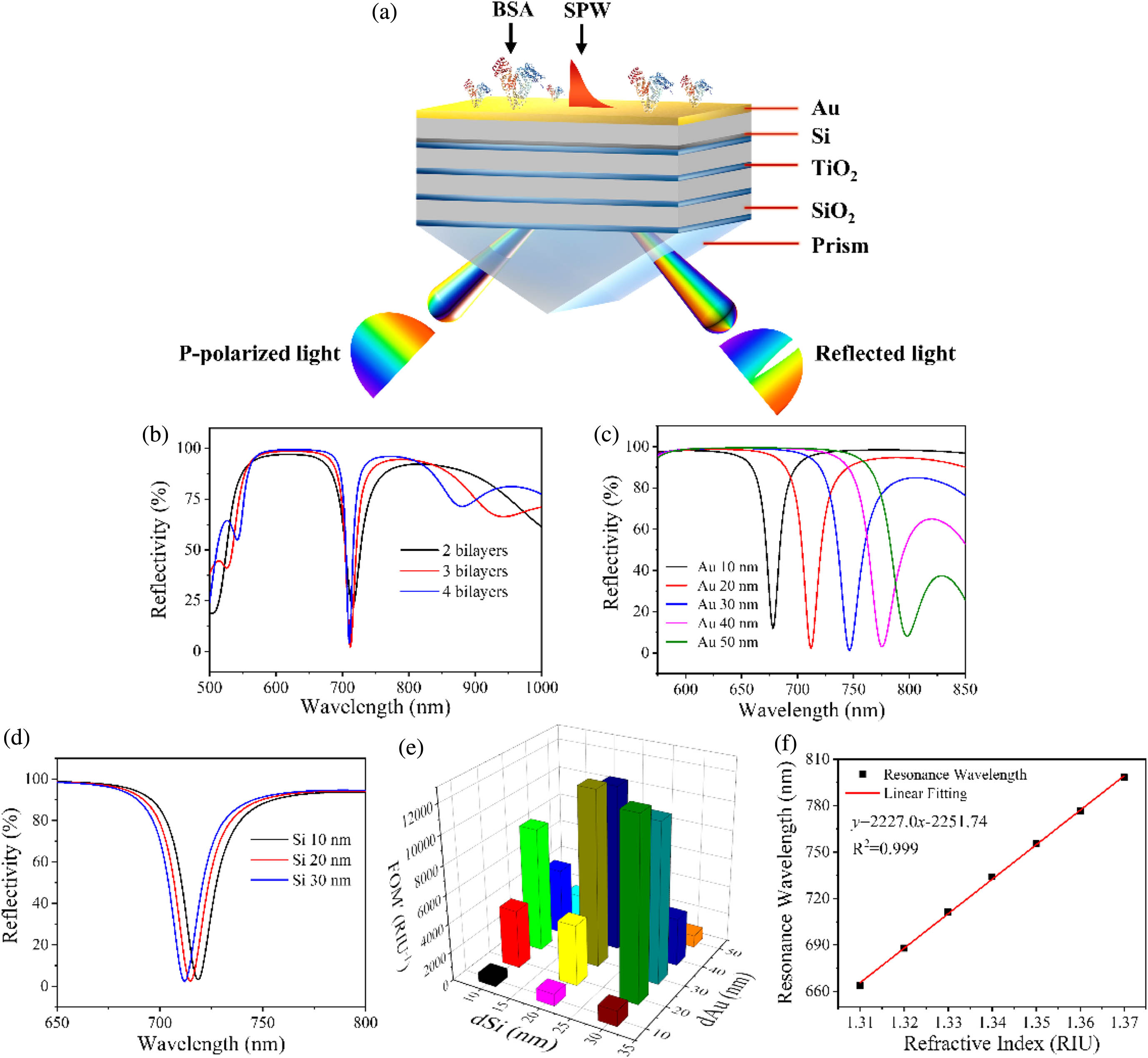
The PC-SPR is based on the Kretschmann configuration, which couples an Au/defect layer/1D-PC composite film with a prism as shown in Fig. 1(a). The 1D-PC comprises N bilayers of high-RI titanium dioxide (, at 632.8 nm) and low-RI silicon dioxide (, at 632.8 nm) that are successively covered with “defect” layers of Si and and an outer layer of Au. The PC-SPR is named for short. An incident light at an angle of 65° is coupled to induce a TIR at the interface between the and Au layers. On the other hand, to form a 1D-PC structure capable of forming a photonic forbidden band (i.e., a highly reflective mirror), the optical path difference of the reflected light needs to be equal to half wavelength () for constructive interference. With Snell’s law (), the thicknesses of the () and () layers are given by , giving rise to and for a center wavelength at an incidence angle of 65°. In this way, a new FP resonator forms in the defect layers in the presence of the two highly reflecting structures.
Figure 1.(a) Schematic diagram of the proposed PC-SPR sensor. Simulated reflectance spectra of the sensor with (b) different bilayers of TiO2/SiO2, (c) different dAu at 30 nm Si layer, and (d) different dSi at 20 nm Au layer. The ambient RI is 1.33 for the simulations. (e) Performance of the sensor with different dSi and dAu. (f) Linear fitting of the resonant wavelength of the optimized PC-SPR device versus ambient refractive index of 1.31–1.37.
The number of bilayers in the PC, thickness of the Au layer, and structure of the defect layer are pivotal in the performance of the PC-SPR sensor. In general, the bilayer increment of the PC leads to a perfect band gap with a high reflectivity, which may facilitate the formation of FP resonance. Therefore, a sensor with different bilayers is first simulated to figure out the potential effect. Since the Au layer strongly affects the SPR, and the defect layers are responsible for the coupling of FP resonance and the SPR, devices with different thicknesses of the Au () and Si () layers are simulated and compared to further optimize sensor performance. For a given , the thickness of silica is given by the following equation to satisfy the FP resonance condition [36]: where is the RI of the Si layer; , are the incident angles of light for the Si and defect layer, respectively; is the Goos–Hanchen shift, where and are RIs of the defect layer and sensing medium, respectively, and is the refraction angle in the substrate.
B. Reflection Simulation
To numerically calculate the optical characteristics of the sensor, the transfer matrix method (TMM) is used in this study. Herein, the reflectance () is represented by a matrix, which is a serial product of the layer matrix and interface matrix ( and ) as follows: where , , and denote the Fresnel reflection coefficient, the wavevector in the direction, and the thickness of the th layer, respectively; and are given by where is the angular frequency, is the light speed in vacuum, and is the optical constant of the th layer.
Figure 1(b) illustrates the simulated reflectance spectra of the sensor with different bilayers of (, ). The device with two pairs of bilayers exhibits a shallow and broad dip, while the one with four pairs of bilayers has the narrowest forbidden band. In contrast, the device with three pairs of bilayers shows a good balance of forbidden band width, dip depth, and FWHM. Therefore, a PC of three bilayers is used hereafter to achieve a relatively high sensitivity in a broad sensing range. Figure 1(c) presents the effect of the Au layer thickness on the reflectance spectra, indicating that the increment of leads to a broadening FWHM, a varied dip depth, and a redshift of the resonance wavelength. By contrast, with the increment of , the FWHM remains unchanged, but the resonance spectrum is blueshifted and the reflectivity shows slight growth [Fig. 1(d)]. For quantizing and optimizing the performance of the PC-SPR sensor, we define the ratio of FOM to as a new figure of merit (FOM’). It is desired to achieve high FOM’ for the PC-SPR sensor, which means a high FOM and a low simultaneously. Figure 1(e) illustrates the FOM’ histogram for different and . Moderate and large are conducive to achieving high FOM’, and the highest FOM’ is obtained at and . The PC-SPR sensor in the following is designed with the optimized thicknesses (, ). By analyzing the simulated reflectance spectra of the designed sensor, a linear relationship between SPR wavelength shift and the liquid RI is demonstrated as shown in Fig. 1(f). The average sensitivity () estimated from the slope of the fitting line is . Considering that the FWHM is 20 nm when the surrounding RI is 1.33, a high FOM value of is achieved for the PC-SPR sensor in the simulation design.
C. Experimental Results and Discussion
The PC-SPR sensor with the optimized structure was fabricated and constructed in a TIR geometry at the incident angle of 65°. It consisted of the 1D-PC and a metallic layer on top of a coupling prism. The and layers were alternately fabricated on a glass substrate using physical vapor deposition. An additional 3 nm chromium layer was deposited on the surface of the prior to Au deposition to increase the adhesion between the and the Au layers. The cross-sectional morphology of the PC-SPR sensor was examined with SEM as shown in Fig. 2(a). The multilayered stacks could be clearly observed. The EDS spectra of the PC-SPR sensor [Fig. 2(b)] and the glass substrate [Fig. 2(d)] indicated that , , Si, and Au were successfully deposited on the glass substrate to form the PC-Au structure.
Figure 2.(a) SEM image of the cross-sectional PC-Au on a glass substrate and (b) the corresponding EDS spectrum. (c) SEM image of the cross-sectional glass substrate and (d) the corresponding EDS spectrum.
To evaluate the performance of the PC-SPR sensor, the fabricated PC-Au/glass was first placed on a prism with index matching oil. A collimated white light from a tungsten–halogen lamp passed through a polarizer to produce a -polarized light that was then projected on the prism at a 65° incident angle. Figure 3(a) shows the reflectance spectra of the PC-SPR sensor in the presence of the sensing liquid with RI ranging from 1.31 to 1.37. The resonance dip is redshifted with the increment of the liquid RI and exhibits a narrow FWHM, e.g., 29 nm FWHM for 1.33 RIU. Further analysis of the spectra demonstrates a good linear relationship between the resonance wavelength and the RI with linearity up to 0.998 in the wide RI range as shown in Fig. 3(b). The average sensitivity is , producing an FOM of for the sensing medium of 1.33 RI.
Figure 3.(a) Reflectance spectra of the PC-SPR sensors for the liquid RI changing from 1.31 to 1.37, (b) linear fitting of the resonant wavelength versus ambient refractive index, (c) reflectance spectra of the 50 nm Au-SPR sensor with the RI ranging from 1.31 to 1.37, and (d) polynomial and linear fitting of the resonant wavelength versus ambient RI.
For comparison of sensor performance, we also fabricated a conventional Au-based SPR (Au-SPR) chip with gold thickness of 50 nm. As shown in Figs. 3(c) and 3(d), the Au-SPR sensor shows smaller shifts of the wavelength resonance and a lower linearity between the resonance wavelength and RI in the range of 1.31–1.37. The fitness of polynomial curve is better than the linear fitting curve, indicating that the RI dependence is nonlinear. Figure 4(a) presents the sensitivities at a specific RI, given by , where and are RI values, and and are the corresponding resonance wavelengths. The calculated sensitivity of the Au-SPR sensor is in the range of , which is much lower than that of the PC-SPR sensor in the range of 2247 to [Fig. 4(a)]. It is noted that the sensitivity of the PC-SPR sensor decreases at 1.36 RI. The reduction is due to the resonance wavelength (833 nm for 1.37 RI) near the boundary of the PC forbidden band [Fig. 1(b)]. In addition, the spectrum of the Au-SPR sensor has a large resonance dip width up to 108 nm in the FWHM. The average FWHM in 1.31–1.37 RI is 98 nm, which is about threefold the FWHM of the PC-SPR sensor [Fig. 4(b)]. The higher sensitivity and narrower resonance spectrum obtained in the PC-SPR sensor resulted in a much greater FOM compared with the conventional Au-SPR sensor as displayed in Fig. 4(c). The average FOM of the Au-SPR sensor is less than , while that of the PC-SPR sensor is up to . Specifically, the PC structure enables a maximum increase of 5.7-fold in FOM at 1.35 RI compared to the conventional SPR sensor [Fig. 4(d)].
Figure 4.Comparison of the Au-SPR and PC-SPR sensors in terms of (a) sensitivity, (b) FWHM, (c) FOM, and (d) average FOM enhancement. The standard deviations are obtained from three tests with different sensors.
The superior performance of the PC-SPR sensor can be attributed to the high reflectivity of the photonic cavity and the TIR boundary between the layer and Au layer. The two highly reflective boundaries allow the formation of an FP cavity in the defect layers. The FP cavity enables effective optical trapping at the resonance mode, some of which can be used to excite SPR in the Au layer. The two modes matching leads to a narrower width of the reflectance spectra [Fig. 4(e)]. The average FWHM (34.3 nm) of the PC-SPR sensor in the range of 1.31–1.37 is approximately one-third of the Au-SPR sensor’s FWHM (98 nm).
Furthermore, the PC-defect structure is found to enhance the field intensity near the Au layer surface. Figure 5 shows the simulated field intensity distributions of the Au-prism and the Au-PC-prism structure. For the Au film/glass structure, the field intensity is enhanced within the Au film but significantly decays on the surface [Fig. 5(a)]. In contrast, by combining the Au film with the PC-defect structure, the incident light intensity is first enhanced by the PC structure and the defect layer and further gains a large amplification in the Au layer. In addition, for a conventional 50 nm Au-SPR sensor, the penetration depth is typically in the range from ten to hundreds of nanometers (about 170.5 nm for this paper) [37], while the penetration depth is up to 2.04 μm. It is well known that the larger penetration depth has a positive effect on the enhancement of the sensitivity of the SPR sensor [38]. As such, the combination of the field intensity enhancement and prolonged penetration depth enables a larger sensitivity and a narrower width of the resonance dip, which result in a 5.7-fold increase of the FOM compared with the traditional SPR sensor.
Figure 5.Distribution of electric field intensity of (a), (c) the conventional 50 nm Au-SPR sensor and (b), (d) the PC-SPR sensor. The field intensity is obtained using finite-difference time-domain (FDTD) simulations provided by the Lumerical Solutions software.
To further verify the capability of RI sensing, a mixture of phosphate buffer and bovine serum albumin (BSA) was flowed through the sensor surface. Figure 6(a) shows the resonance spectra with different concentrations of BSA (0 to ). The resonance wavelength is redshifted in a good linear relation with the BSA concentrations [coefficient , Fig. 6(b)], achieving an average sensitivity of for the PC-SPR sensor.
Figure 6.Reflectance spectra for the PC-SPR sensors versus BSA concentration ranging from 0 to . (b) Linear fitting of the average resonant wavelength for different BSA concentrations; the standard deviations are obtained from three tests with different sensors.
A performance comparison between the proposed PC-SPR sensor and the other SPR sensors is summarized in Table 1 in terms of detection range, sensitivity, FWHM, and FOM. The PC-SPR sensor exhibits a superior performance compared to other SPR sensors that are constructed using silver, bimetallic layers, or a composite layer of metal and nanostructured nonmetallic materials (e.g., porous silica, titania, and zirconia gratings) [39–43]. A higher FOM than that of the PC-SPR sensor can be achieved by employing metamaterials such as Au mushrooms [20], Au hyperbolic metamaterial (HMM) and 2D grating [22], and 2D periodic plasmonic structure-Au [19]. However, these sensors require expensive nanoscale photolithography for metamaterial fabrication. In comparison, the PC-SPR can be easily constructed by an alternative deposition. The simple 1D–composite layer structure provides a 5.7-fold increase in FOM compared to the conventional Au-SPR sensor. Indeed, the FOM of the PC-SPR sensor can be further optimized by increasing the number of dielectric pairs of the PC or/and depositing nanomaterials on the metallic layer surface [13,44–46].
Plasmonic interface
Detection range (RIU)
Sensitivity (nm·RIU−1)
FWHM (nm)
FOM (RIU−1)
Theoretical/Experimental
Refs.
Ag-porous silica
—
42.9 deg · RIU−1
0.505 deg
85.0
Theoretical
[39]
Au-oxide grating
1.332–1.372
940
15
62.5
Experimental
[42]
Al-Cu
1.333–1.35
2300–3100
103–121
19–30
Experimental
[40]
Ag
1.3–1.40
1523–4365
39.3–87.7
38.8–51.6
Experimental
[41]
ITO-Ag
1.33–1.36
—
—
39
Theoretical
[43]
Au mushrooms
1.333–1.417
1010
10
108
Experimental
[20]
Au HMM
—
30,000
50.8
590
Experimental
[22]
2D plasmonic array
—
2190
3
730
Experimental
[19]
Au film
1.31–1.37
1266–2161
98
17.6
Experimental
This work
PC-Au
1.31–1.37
2247–2994
30
73.7–103.2
Experimental
Table 1. Comparison of the PC-SPR Sensor and Other SPR Sensors
We have demonstrated a novel technique to improve the FOM of an SPR sensor based on the structure of . The new SPR sensor integrates the Au layer with the 1D-PC () and defect layers (). The PC can effectively couple the light into the defect layer to form FP resonance and excite SPR in the gold layer, which allows for a narrow reflection spectrum and a significant increment of electric field on the sensing surface. The optimized PC-SPR sensor presents an average sensitivity of in the experiments and achieves up to 5.7 times improvement of FOM as compared to that of the conventional 50 nm Au-SPR sensor. With respect to RI detection of the BSA solutions, the PC-SPR sensor displayed an average sensitivity of in the presence of BSA solution. This paper paves a new and simple way to enhance the SPR sensor performance. We believe that the PC-SPR sensor can be further optimized by engineering the PC structure and materials, and that it holds potential in sensitive detection of bio- and chemical analytes.