1The Guo China-US Photonics Laboratory, State Key Laboratory of Applied Optics, Changchun Institute of Optics, Fine Mechanics and Physics, Chinese Academy of Sciences, Changchun 130033, China
2University of Chinese Academy of Sciences, Beijing 100049, China
3State Key Laboratory of Luminescence and Applications, Changchun Institute of Optics, Fine Mechanics and Physics, Chinese Academy of Sciences, Changchun 130033, China
4The Institute of Optics, University of Rochester, Rochester, New York 14627, USA
Bin Wang, Chen Zhao, Huanyu Lu, Tingting Zou, Subhash C. Singh, Zhi Yu, Chaonan Yao, Xin Zheng, Jun Xing, Yuting Zou, Cunzhu Tong, Weili Yu, Bo Zhao, Chunlei Guo, "SERS study on the synergistic effects of electric field enhancement and charge transfer in an Ag2S quantum dots/plasmonic bowtie nanoantenna composite system," Photonics Res. 8, 548 (2020)
Copy Citation Text
Localized surface plasmon resonance (LSPR) of nanostructures and the interfacial charge transfer (CT) of semiconductor materials play essential roles in the study of optical and photoelectronic properties. In this paper, a composite substrate of quantum dots (QDs) coated plasmonic Au bowtie nanoantenna (BNA) arrays with a metal–insulator–metal (MIM) configuration was built to study the synergistic effect of LSPR and interfacial CT using surface-enhanced Raman scattering (SERS) in the near-infrared (NIR) region. The Au BNA array structure with a large enhancement of the localized electric field (E-field) strongly enhanced the Raman signal of adsorbed p-aminothiophenol (PATP) probe molecules. Meanwhile, the broad enhanced spectral region was achieved owing to the coupling of LSPR. The as-prepared Au BNA array structure facilitated enhancements of the excitation as well as the emission of Raman signal simultaneously, which was established by finite-difference time-domain simulation. Moreover, semiconductor QDs were introduced into the BNA/PATP system to further enhance Raman signals, which benefited from the interfacial CT resonance in the system. As a result, the Raman signals of PATP in the system were strongly enhanced under 785 nm laser excitation due to the synergistic effect of E-field enhancement and interfacial CT. Furthermore, the SERS polarization dependence effects of the system were also investigated. The SERS spectra indicated that the polarization dependence of the substrate increased with decreasing polarization angles of excitation from p-polarized excitation to s-polarized excitation. This study provides a strategy using the synergistic effect of interfacial CT and E-field enhancement for SERS applications and provides a guidance for the development of SERS study on semiconductor QD-based plasmonic substrates, and can be further extended to other material-nanostructure systems for various optoelectronic and sensing applications.
1. INTRODUCTION
Having unique characteristics, such as a nondestructive nature, ultrahigh sensitivity, and molecular specificity, surface-enhanced Raman scattering (SERS) has been widely explored in analytical detection, molecular imaging, Raman mapping, environmental monitoring, and material investigation since it was first demonstrated on silver electrodes in the 1970s by Martin Fleischmann, Patrick J. Hendra, and A. James McQuillan. It has since been investigated by several other researchers [1–3]. The inherent benefits of SERS in the near-infrared (NIR) region, such as reduced photo-bleaching, a low fluorescence background, and a greater penetration depth into biological macromolecules for NIR excitation, make it a powerful tool for biodetection and biosensing [4–7]. Two widely accepted mechanisms, the electromagnetic mechanism (EM) and the chemical mechanism (CM) were used to explain the SERS phenomenon [8]. The EM is believed to make the most contribution to SERS, where the electric field (E-field) is strongly enhanced in the localized area, forming “hot-spots” through plasmonic coupling of EM radiation with localized surface plasmon resonance (LSPR) of metallic nanostructures [9,10]. Another contribution to the SERS phenomenon is the charge transfer (CT) mechanism, which involves the transfer of an electron either from the Fermi level of a metal or from a semiconductor through interband transition to an unoccupied molecular orbital of probe molecule [11,12]. The SERS selection rules must be matched to produce resonance effects, including molecular resonance and molecule–semiconductor CT resonance belonging to CM, and such electromagnetic resonance as metal-like surface plasmon resonance and Mie scattering resonance belonging to EM under an excitation laser [13].
Metal nanoparticles or nanostructures are mostly used as SERS substrates and exhibit great SERS enhancement through EM. These substrates can produce strong plasmonic resonances due to coherent oscillations of electrons driven by an incident E-field [14]. These plasmonic systems are able to confine the E-field in the sub-wavelength region and provide extremely enhanced Raman signals [15,16]. Ordered nanoparticles arrays can be prepared to produce strong E-field enhancement for SERS measurements based on self-assembly methods and nanofabrication techniques [17]. However, different from nanoparticles arrays, intelligently designed metallic nanostructures exhibit outstanding properties, including large tunability of spectral responses from the ultraviolet (UV) to the NIR region and extreme enhancement of the localized E-field due to LSPR coupling, and produce distinct SERS intensity and enhancement factors in the wide spectral range [18–20]. Plasmonic nanoantenna is one of the most used metal nanostructures for SERS study and various antenna designs, such as Yagi–Uda antennas, spiral nanoantennas, and U-/T-shaped nanoaperture antennas; nanodisc, nanorod, and nanocube antennas have been developed and used for optical and sensing applications including biochemical sensing [21,22], spontaneous emission enhancement [23,24], solar energy conversion [25,26], and nanoscale light sources [27,28]. In particular, owing to its triangular shape, the bowtie nanoantenna (BNA) can provide an efficient LSPR coupling between the triangle tips to generate a strong locally enhanced E-field in the nanogap different from other geometric nanostructures [29–31]. As a result, the Raman scattering intensity of molecules located near the nanotip and in the nanogap of the BNA can be strongly enhanced by several orders of magnitude resulting in strong SERS [32–34]. Recently, a metal-insulator-metal (MIM) system, where a metallic nanostructure and a metallic thin film are separated by a dielectric spacer, has been studied extensively for plasmonic applications [35,36]. In plasmonic nanoantennas with MIM structures, the flexibility to tune E-field enhancement and spectral response is mainly attributed to the coordinated multiple coupling (i.e., the in-plane near-field coupling, the in-plane far-field coupling, and the out-of-plane coupling) [37,38]. Besides extreme enhancement of E-field by LSPR coupling in the gap region, the BNA possesses other advantages, including directionality, highly efficient electro-optical driving, and polarization control over other coupled dipole antenna designs [39,40]. Owing to these virtues, the BNA with an MIM structure is expected to exhibit great scientific interest and has led to a few exciting applications in nanophotonics, including SERS and biosensing.
In addition to the extensive SERS study by EM on the formation of hot spots by different structural geometries, the CM is mainly attributed to the interfacial CT between probe molecules and substrate materials, which continues to be of great importance for SERS [41]. When the excitation wavelength matches with one of the CT processes, chemical enhancement of specific Raman modes can be observed. The Herzberg–Teller surface selection rule is the most comprehensive and widely accepted approach to explain the CT effect [42]. In recent years, owing to the CT mechanism, the materials for SERS studies are being gradually extended from noble metals and transition metals to semiconductor materials, such as metal oxide, two-dimensional (2D) materials, and semiconductor quantum dots (QDs), where SERS performance was largely improved by various semiconductor substrates [43–45]. QDs used in the SERS study especially show excellent properties such as high quantum yield, a tunable bandgap, and high stability [46–48]. As narrow bandgap semiconductors, silver sulfide QDs have many excellent properties, such as broadband optical response, a high absorption coefficient, strong chemical stability, nontoxic properties, and excellent emission in the second NIR region (wavelength from 1000 to 1350 nm) [49]. It has also been widely considered as a potential candidate for optoelectronics, energy harvesting, and sensing applications [50,51]. The application of QDs is mainly focused as NIR fluorescent probes for in-vivo imaging, and in the fabrication of the solar cells of QDs, thin-film transistors, optical detectors, infrared biological sensors, and optical filters [52–54]. However, uses for QDs and its composite as a SERS substrate are limited [46,50,55–57].
Sign up for Photonics Research TOC. Get the latest issue of Photonics Research delivered right to you!Sign up now
Usually, EM enhancement is several orders of magnitude stronger than CM enhancement (including molecular resonance and CT resonance). However, whether EM–SERS enhancement or CM–SERS enhancement, the individual contribution for SERS is usually unsatisfactory. In this work, we studied the synergistic effect of CT resonance at the interface of BNA–QDs–PATP (p-aminothiophenol) and E-field enhancement around BNA arrays for SERS in the NIR spectral region using a semiconductor–QDs/metal-nanostructure composite substrate. Under 785 nm laser excitation, the Au BNA arrays with an MIM structure provide a strongly localized and enhanced E-field that coupled with a CT process at the interface of BNA–QDs–PATP to get strong Raman enhancement. The broadband LSPR coupling of plasmonic BNA arrays can provide E-field enhancements at excitation as well as Raman scattering wavelengths. Furthermore, the SERS polarization dependence effects of the system are also studied. The polarization dependence study showed an increase in the SERS intensity with decreasing polarization angles of excitation from p-polarization () to s-polarization (). The finite-difference time-domain (FDTD) simulation was performed to calculate spectral E-field enhancement and spatial distribution of E-field at excitation wavelength around BNA arrays. The present study provides a guidance for the development of a composite metal–semiconductor system that could synergistically harness the strong E-field enhancement capability of metallic nanostructures and CT characteristics of semiconductors to enhance optoelectronic, electro-optical, solar energy, and sensing efficiency of different devices.
2. EXPERIMENTAL METHODS
A. Materials
Sulfur powder (S, 99.95%) was purchased from Fuchen (Tianjin) Chemical Reagent Co., Ltd. Silver nitrate (, 99.9995%) and oleic acid (OA, technical grade, 90%) were purchased from Sinopharm Chemical Reagent Co., Ltd. Tri-n-octylphosphine (TOP, technical grade, 90%), 1-octadecylamine (ODA, technical grade, 90%), and 1-octadecene (ODE, technical grade, 90%), were purchased from Aladdin Industrial Corp. Methyl alcohol (99.5%), ethyl alcohol (99.7%), butyl alcohol (99.5%), hexanes (98%), acetone (99.5%), and methylbenzene (99.5%) were purchased from Beijing Chemical Industry Group Co., Ltd. P-aminothiophenol (PATP, 98.0%) was purchased from Shanghai Yuanye Bio-Technology Co., Ltd. All chemicals were used as delivered without further purification.
B. Synthesis of Quantum Dots
For the synthesis of quantum dots [51], 16.99 g of was dissolved separately in 100 mL tri-n-octylphosphine (TOP) to obtain Ag-TOP. A mixture of 6.4 mL of oleic acid (OA), 5.4 g of 1-octadecylamine (ODA), 12.8 mL of 1-octadecene (ODE), and 72 mg of sulfur powder was then combined in a 100 mL round-bottom flask, degassed, flushed three times with to remove water and oxygen, and heated to 70°C under until the powders dissolved. Then 4 mL of Ag-TOP was quickly injected at 197°C, and the reaction was allowed to proceed for 12 min at 167°C. The growth was quenched in an ice bath, and 25 mL of butanol was added to prevent solidification of the reaction mixture as it cooled. The nanocrystals were isolated by precipitation with ethanol and redispersed in hexane. To remove excess ligands and impurities in the raw materials, the synthesized QDs were further purified. The purification process was as follows: 30 mL of methanol was added into 5 mL of the product, and the resulting mixture was thoroughly mixed through vigorous ultrasonication followed by separation of the product through centrifugation. The centrifuged product was redispersed into 2 mL of toluene through ultrasonication followed by addition of 30 mL of methanol, further ultrasonication for 30 min, and separation of the product through centrifugation. This step was repeated three times to remove impurities and excess ligands and solvents. The methanol was then replaced by acetone and the purification process was repeated for two more cycles. After five purifications, the QDs were dispersed in n-hexane for use.
C. Fabrication of the Nanostructure
A 100 nm thin gold film was first deposited on the substrate (300 nm thick on the top of the silicon wafer) using a high vacuum resistance evaporation coating system. Then, a 20 nm of silica spacer layer was deposited on the surface of the gold film using a plasma-enhanced chemical vapor deposition (PECVD) system. Next, a photoresist layer was spin-coated on the surface of silica (20 nm) and patterned using an electron beam lithography (EBL) system. A 100 nm thick gold film was next deposited on the surface of the photoresist that has been developed. Finally, a lift-off process was used to fabricate the structure.
D. QDs Coated and PATP Modified Sample and Its Characterization
QDs were deposited on the surface of a wafer, Au film, and BNA arrays substrates by spin-coating at 2500 r/min for 35 s in an air environment. The coated sample was immersed in a PATP solution (dissolved in alcohol) for 2 h followed by cleaning with alcohol and drying under a flow.
The Raman spectra were collected using a LabRAM HR Evolution Raman spectrometer (Horiba Jobin Yvon). The laser beam was focused on a spot approximately 1 μm in diameter using an objective microscope with magnification. The data acquisition time was 5 s for all systems. The UV-Vis spectral measurements were carried out using a Cary 5000 UV-vis-NIR spectrometer (Agilent). X-ray diffraction (XRD) spectra were collected using a Bruker D8 FOCUS X-ray diffractometer. Scanning electron microscopy (SEM) and energy dispersive spectroscopy (EDS) analysis was done by the scanning electron microscope (Phenom ProX). X-ray photoelectron spectroscopy (XPS) data were obtained using an X-ray photoelectron spectrometer (Thermo ESCALAB 250Xi). Transmission electron microscopy (TEM) images of QDs were taken using a JEOL JSM- 6700F transmission electron microscope. The relative standard deviation (SD) data of the main vibrating peaks, intensity from five randomly chosen spots in the same sample are used in the calculation of the CT degree and Raman intensity to evaluate the signal reproducibility.
E. FDTD Simulations
For the simulations, we employed an FDTD method based on Yee’s algorithms [58] for electromagnetic simulation. In the FDTD method, Maxwell’s equations are discretized in both time and space, and the central difference approximation is used. A commercial FDTD package from Lumerical Inc.’s DEVICE Suite was used to calculate spectral response and E-field distribution of BNA arrays. A perfectly matched layer (PML) was used in the -axis direction, while periodic boundary conditions were used in the - and y-axis directions. The designed plasmonic system was allowed to illuminate with a polarized plane wave propagating along the axis. Two different polarization states for the incident electromagnetic wave, the s-polarization, E-field parallel to the axis (along the antenna axis), and the p-polarization, E-field parallel to the axis (normal to the antenna axis), were used in the FDTD simulations to investigate the light polarization effects on the SERS enhancement. Two detector boxes were placed to measure the distribution of E-field in the and planes. For the calculation of SERS maps, the data of the E-field distribution were extracted from detector boxes at the wavelength of excitation and Raman vibrational modes. SERS maps of E-field intensity distribution [] were plotted by MATLAB (R2014b). An ultrafine mesh size (1 nm) was used in all the simulations. The refractive index of is chosen for air to generate an asymmetric environment. The optical constants of Au, , and Si were taken from Ref. [59].
3. RESULTS AND DISCUSSION
A. Characterization of Quantum Dots
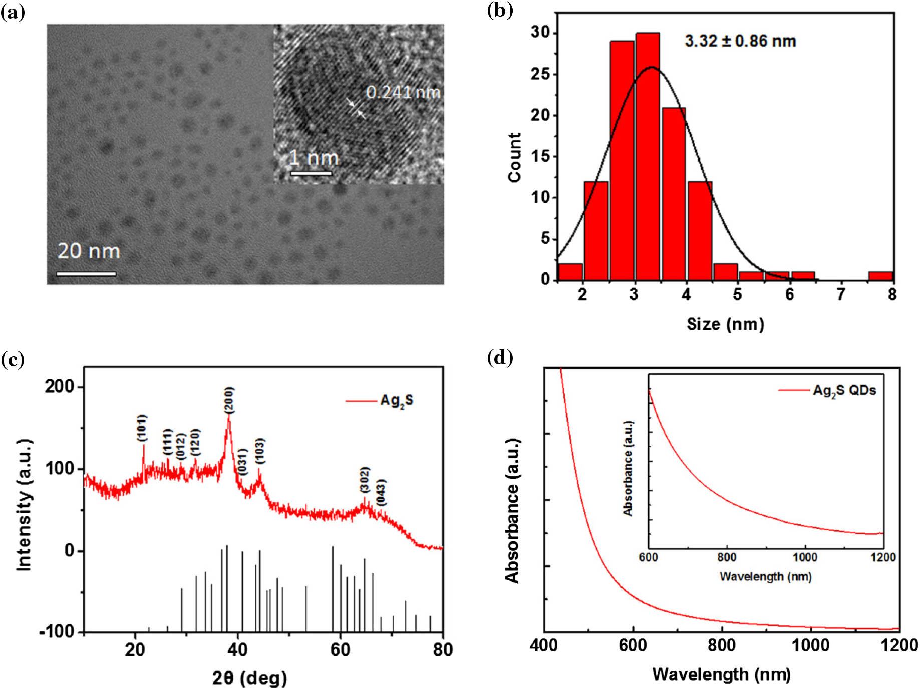
TEM images of the QDs are shown in Fig. 1(a), while the inset shows a representative high-resolution TEM (HRTEM) image of a quantum dot with lattice spacing of 0.241 nm. Figure 1(b) exhibits the particle size distribution of QDs by histogram. It shows that the majority of as-prepared QDs were spherical or spheroidal in shape, with an average size of 3.32 nm and a narrow size dispersion of 0.86 nm. Figure 1(c) shows the XRD characterization result of the as-prepared QDs. Almost all of the peaks in the XRD patterns matched those of monoclinic [46]. To further investigate the purity and composition of coated BNA arrays, XPS images were also studied (see Appendix A). Figure 1(d) shows the UV-vis-NIR absorption spectrum of QDs, which indicates a broad absorption range until the NIR region.
Figure 1.Characterization of QDs. (a) TEM image of QDs (scale bar 20 nm). Inset shows an HRTEM image of a QD with a lattice spacing of 0.241 nm (scale bar 1 nm). (b) Histogram for the size distribution of QDs with average size of 3.32 nm. (c) XRD spectrum of the QDs with JCPDS data. (d) UV-vis-NIR absorption spectra of the QDs.
B. Characterization of Au Bowtie Nanoantenna Arrays
Figure 2(a) shows the SEM image of the Au BNA arrays with an enlarged view in the inset. The BNA arrays consist of a periodic arrangement of a pair of equilateral triangles (known as a bowtie) as a unit cell. The side length of equilateral triangle is 420 nm, and the gap distance between a pair of equilateral triangles is 160 nm. The separation between two-unit cells (transverse period) is , and the separation between two lines made of BNA (vertical period) is μ. The EDS confirmed the elemental contents of the QDs coated Au BNA arrays substrate, shown in Fig. 2(b). Insets of Fig. 2(b), from left to right, show the scanned region for EDS, and elemental mapping of S, Ag, and Au. From the EDS mapping of S [(inset (ii)] and Ag [inset (iii)] in the scanned region, we can say that the QDs are uniformly distributed on the surface of BNA substrate.
Figure 2.Characterization of Au BNA arrays. (a) SEM images of the BNA arrays (scale bar 2 μm). Inset shows an enlarged view of three pairs of BNA (scale bar 300 nm). (b) EDS analysis of QDs on BNA arrays. On the top, from left to right: (i) scanned region for EDS, and elemental mapping of (ii) S, (iii) Ag, and (iv) Au. Inset shows the elemental composition of different elements in BNA arrays/Ag2S-QDs substrate.
C. Theoretical Modeling of Au Bowtie Nanoantenna Arrays
The theoretical modeling is performed using full-wave simulation with the FDTD method (Lumerical Inc.). A 3D model is used to study the E-field enhancement calculated as , where is the incident laser field and E is the resulting near field. An s-polarized plane wave (E-field direction parallel to the axis) is used in the simulation. The plasmonic BNA arrays locate above the 100 nm Au thin film separated by a 20 nm spacer layer on the substrate (300 nm on the top of Si wafer), as displayed in Fig. 3(a), and the shape of BNA is an equilateral triangle. The parameters of the BNA arrays, as obtained by the SEM image [Fig. 2(a)], include a side length of 420 nm, a gap distance of 160 nm, a triangle thickness of 100 nm, a transverse period of 580 nm, and a vertical period of 2 μm consistent with the experiment result.
Figure 3.Schematics and calculated E-field distribution of Au BNA arrays. (a) Geometrical parameters of BNA arrays with MIM structure. (b) E-field enhancement of the BNA arrays at point. Inset shows the enlarged E-field enhancement spectrum range from 780 to 930 nm. (c)–(e) E-field distribution () in plane at three LSPR modes.
Figure 3(b) shows the E-field enhancement spectrum of the BNA arrays with MIM structure at the center of the bowtie gap ( point, inset), which exhibits three distinct peaks corresponding to different LSPR modes. The primarily mode corresponding to the dipolar LSPR mode, located around 802 nm with the largest E-field enhancement, is close to the pump wavelength at 785 nm used in SERS measurements. The E-field of the mode is mainly localized in the bowtie gap, which is caused by LSPR coupling between closely spaced nanoprisms, as shown in Fig. 3(c). Moreover, a moderate level of E-field enhancement is also observed around the outer corners and edges of the triangles. The large spatial distribution of the E-field enhancement at 802 nm shows comparatively larger available surface regions for E-field-based SERS with excitation close to this wavelength [Fig. 3(c)]. The other two higher-order LSPR modes are located at 726 nm () and 686 nm () with a comparatively lower E-field enhancement. The E-fields of these two modes are localized in the gap and outer corners of nanoprisms [Figs. 3(d) and 3(e)] [60]. The E-field distribution of three LSPR modes in the plane and the distribution of the E-field enhancement at 802 nm ( mode) along the , , and directions are discussed in detail (see Appendix B). The inset curve in Fig. 3(b) shows an enlarged view of the E-field enhancement spectrum in the spectral range of 780 to 930 nm that includes an excitation laser wavelength of 785 nm used in the SERS study, as well as Raman scattering modes used in SERS measurements [wavelengths range from 837 nm (or ) to 914 nm (or ), the starting and ending points of SERS measurements] of PATP probe molecules. The enhancement factor (EF) of a SERS substrate is defined as (i.e., the product of the near field enhancement at the excitation and Stokes wavelengths) [61]. Therefore, a broadband LSPR absorption ranging from excitation wavelength to Raman scattering signal in a plasmonic system is important to get high E-field EF in SERS. The position of the first resonant mode with its peak (, 802 nm) close to the excitation wavelength (785 nm) along with a broadband E-field enhancement covering the region of Raman scattering of the probe molecule makes the designed plasmonic system an ideal candidate to enhance the E-field of excitation as well as Raman scattering signals for E-field-enhancement-based SERS measurements.
D. SERS Spectra of PATP Molecules Adsorbed on QDs Coated BNA Arrays
Figure 4 shows the Raman spectra of PATP molecules adsorbed on QDs coated BNA arrays [Fig. 4(a)] compared to those that are separately on bare BNA arrays [Fig. 4(b)] and QDs [Fig. 4(c)] under 785 nm laser excitation. Raman spectrum of PATP powder on the glass slide is also presented as a reference [Fig. 4(d)]. As can be seen from Fig. 4, there is no Raman signal achieved when PATP molecules are adsorbed on QDs [Fig. 4(c)]. In addition, the Raman signal of PATP molecules adsorbed on BNA arrays [Fig. 4(b)] is also very weak. However, for PATP molecules adsorbed on QDs coated BNA arrays [Fig. 4(a)], the Raman signals are extremely enhanced. The Raman bands located at [, 18a], [, 7a], and [, 9a] are assigned to the mode while [, 9b], [, 14], [, 3], [, 19], and [, 8b] are assigned to the mode of the PATP molecule. A more detailed band assignment for the SERS spectrum of PATP under different conditions is summarized in Table 1 [62].
Figure 4.Raman spectra of PATP molecules adsorbed on a different substrate. (a)–(c) Raman spectra of PATP molecules adsorbed on QDs coated BNA arrays (red curve), BNA arrays (black curve), and QDs (blue curve), respectively. (d) Raman spectrum of PATP powder as reference. The spectra were collected under 785 nm laser excitation. Raman spectra are shifted compared to each other along the axis for better viewing.
E. SERS Investigation of Synergistic Effects Between Charge Transfer and Electric Field Enhancement
The extremely enhanced Raman phenomenon in our study is attributed to the synergistic effects of both E-field enhancement from the BNA arrays and the CT resonance at the interface of the BNA–QDs–PATP composite system.
First, the large enhancement of the localized E-field, which is caused by the LSPR of BNA arrays, is one of the key factors that contribute to the Raman enhancement. To investigate the effect of the E-field on the SERS enhancement, we compared the SERS signal of PATP molecules adsorbed on the BNA arrays and Au thin film (30 nm). As shown in Fig. 5(a), the SERS signal of the BNA/PATP system is strongly enhanced, especially at [, ], compared to that of the Au-film/PATP system, where a detectable Raman signal is not observed. It is because the BNA arrays possess a strong E-field enhancement under 785 nm laser excitation, which is near the mode (802 nm) of BNA arrays. Moreover, the E-field of the mode () that is one of the most intense vibrational Raman modes of the PATP molecules, also gets strongly excited by BNA. The spatial distributions of the enhanced E-field of BNA in the and planes under 785 nm laser excitation are shown in Figs. 5(b) and 5(c), respectively. It can be seen from Fig. 5(b) that the E-field is mainly distributed in the central gap region with extreme enhancement, which is due to the hot spots effect generated by the LSPR coupling of a single BNA. The enhanced E-field is also distributed around the corners of triangles, which benefits from the interaction of the tip impact and pairs of BNA. The spatial distribution of the E-field in the plane [Fig. 5(c)] exhibits an E-field with strong field intensity localized in an almost entire air gap formed by tip-to-tip triangles. Meanwhile, an enhanced E-field is confined below both the tips and the ridges of the BNA, which is supported by the mode coupling of the Fabry–Perot cavity formed along the -axis in the 20 nm thin spacer layer sandwiched between two layers of gold. The spatial distribution of the SERS EF (or SERS maps) for the bands located at [, ] and [] of the PATP molecule is shown in Fig. 5(d) (top view: plane) and Fig. 5(e) (side view: plane), respectively. The SERS E-field EFs are and for and Raman vibrational modes, respectively. Thus, it can be concluded that the BNA arrays can provide a strong enhanced E-field for SERS enhancement.
Figure 5.Raman spectra of PATP molecules adsorbed on Au film and BNA substrates and the spatial E-field distribution of the BNA. (a) Raman spectra of the PATP molecules adsorbed on the BNA arrays (red curve) and 30 nm Au film (blue curve) under 785 nm laser excitation. (b), (c) Spatial E-field distribution () of the BNA in the and planes under 785 nm laser excitation, respectively. (d), (e) Spatial distribution of E-field EF corresponding to (or 857 nm) and (or 862 nm) vibrational modes of PATP in the plane and plane, respectively. In the plots (d) and (e), the white dashed lines represent the BNA for the SERS E-field EF calculation; the excitation wavelength was considered as 785 nm. Raman spectra are shifted compared to each other along the axis for better viewing.
Another interesting phenomenon is that after the deposition of QDs onto the surface of BNA arrays, the SERS signal of the adsorbed PATP molecules was further enhanced compared to the Raman spectra of PATP molecules adsorbed on both QDs and BNA due to the combined effects of BNA and QDs. Herein, the enhanced Raman signal is not only affected by the E-field of the BNA; the QDs also play a key role in the enhancement. As shown in Fig. 4, compared to the bulk Raman signal of PATP [Fig. 4(d)] and the SERS signal of the BNA/PATP system [Fig. 4(b)], there are several bands assigned to the mode of the PATP molecules, such as the1138, 1299, 1388, 1435, and bands, which are selectively enhanced in the SERS spectrum of the system. These selectively enhanced modes indicate that the CT process takes place at the interfaces of the BNA–QDs–PATP composite system, which is proven by the Herzberg-Teller contributions [42]. The CT mechanism is further explained by the complete energy level diagram under the 785 nm laser excitation in Fig. 6. The energy levels for the conduction band (CB) and the valence band (VB) of QDs are 3.63 and 5.32 eV, respectively [63,64]. The highest occupied molecular orbital (HOMO) and the lowest unoccupied molecular orbital (LUMO) of PATP molecules are 7.16 and 3.03 eV, respectively [65,66]. The Fermi level () of gold is 5.1 eV. Figures 6(a) and 6(b) show the energy level diagram of the Ag2S–QDs/PATP and Au–BNA/PATP composite, respectively. The photon energy of the 785 nm laser (ca. 1.58 eV) is too low to excite the electronic transitions between the band levels at the interfaces of Ag2S–QDs/PATP (ca. 1.69 eV) and Au–BNA/PATP (ca. 2.07 eV). Therefore, the direct CT resonance is not easily achieved at the interface of both systems because of the larger energy difference [Figs. 4(b) and 4(c)]. However, for the system [Fig. 6(c)], the photon energy of the 785 nm laser (ca. 1.58 eV) can match the band−band transition energy of the interface (ca. 1.47 eV). The electrons in the Fermi level of Au can be photoexcited into the CB of the QDs under 785 nm excitation. Subsequently, dynamic CT could occur by coupling with the vibrations of the molecules to easily transfer an electron to the LUMO level of a PATP molecule. This results in a similar “donor–bridge–acceptor” CT mode, which occurs more easily in the system due to the principle of energy level matching [66–68]. So the CT resonance can take place at the interfaces of the BNA–QDs–PATP system under 785 nm excitation [Fig. 4(a)]. As a result, the SERS signal of the adsorbed PATP molecules gets further enhanced.
Figure 6.Energy level diagram of (a) , (b) Au-BNA/PATP, and (c) systems under 785 nm laser excitation, respectively.
To further evaluate the synergistic effects of the E-field and CT to the SERS enhancement, the SERS spectra of the PATP molecule adsorbed on the QDs coated BNA arrays and QDs coated Au thin film (30 nm) were compared. First, as shown in Fig. 7(a), the b2 modes of these two complex systems were selectively enhanced under 785 nm laser excitation, which ascribed to the CT mechanism in both systems. The degree of charge transfer was used to investigate the CT contribution in the SERS enhancement [11,69]. The of a -bond can be determined using where the index “” represents individual lines in the SERS spectra. For a nonsymmetric line, is usually quite small or zero. We defined as the intensity of the band ( mode) and as the intensities of the bands at 1138, 1388, 1435, and ( mode), which are derived from nonsymmetric contributions. The degrees of CT for PATP in both and systems at 1138, 1388, 1435, and with excitation at 785 nm are shown in Fig. 7(b). The CT value calculated by these peaks shows no obvious difference in these two systems, which indicates that these two systems possess nearly the same CT degrees, and the surface nanostructure of BNA will not affect the CT of the system. So the CT mechanism shows the same contribution to these two systems. However, as shown in the Fig. 7(a), the intensity of the Raman signal in the system is much stronger than that in a system. Notice that the signal of PATP adsorbed on QDs coated Au film is magnified 10 times. Such enhancement of the SERS signals in the BNA–QDs–PATP system compared to the Au film–QDs–PATP system can be attributed to the huge localized E-field of BNA arrays, as discussed above. Thus, we can conclude that the SERS enhancement of the BNA–QDs–PATP arises from the synergistic effects of the E-field and the CT mechanism.
Figure 7.Raman spectra and degree of charge transfer of different composite systems. (a) Raman spectra of the PATP molecule adsorbed on QDs coated BNA arrays (red curve) and QDs coated Au thin film (30 nm) (blue curve). (b) Degree of charge transfer (CT) of the PATP adsorbed on coated Au film and coated BNA arrays at modes with excitation at 785 nm. Raman spectra are shifted compared to each other along the axis for better viewing. Error bars represent [, ].
The SERS EF for the PATP probe molecule is roughly calculated (see Appendix C) to evaluate the enhancement ability by the Raman intensity of the band at [, ] in the system. The EF value is estimated to be about , which is attributed to the synergistic effects of the E-field enhancement and CT. To further estimate the enhancement ability of the synergistic effects in the system, we compared the Raman intensities of the bands at [, ] and [] in the BNA/PATP, , and systems [see Appendix C, Figs. 11(c) and 11(d)]. For the vibrational mode at [], the Raman intensity of the system shows a 432% enhancement over the BNA/PATP system and a 3449% enhancement over the system. Moreover, for [, ], the Raman intensity of the system shows a 1669% enhancement over the BNA/PATP system and a 4700% enhancement over the system. Thus, the synergistic effect of the E-field enhancement and CT results in the largest enhancement for the -arrays system. The mapping analysis obtained by the band at indicates that the Raman enhancement in the system under 785 nm laser excitation is much stronger near the BNA array compared to the enhancement at the non-BNA regions, which is consistent with the simulated enhancement of the E-field (see Appendix D). Meanwhile, to further study the synergistic effects of the E-field enhancement and CT, we measured the SERS spectra of the , BNA/PATP, and systems under 473 and 532 nm excitation wavelengths (see Appendix E). The synergistic effects of the E-field enhancement and CT resonance make the SERS intensity larger under 532 nm laser excitation compared to the 473 nm laser excitation.
F. SERS Polarization Dependence Effects of BNA and QDs Coated BNA Arrays
Moreover, we studied the SERS polarization dependence effects of PATP adsorbed on BNA and QDs coated BNA arrays. As discussed earlier, the SERS intensity is influenced by the EM and CT processes. Therefore, the influence of polarized light on the E-field intensity and CT process will directly lead to a change in the Raman intensity. Figure 8(a) shows the SERS spectra for PATP adsorbed on BNA arrays under different polarization angles of light excitation (785 nm laser excitation). One can see that the SERS intensity is strongest under s-polarized (, E-field oscillation along the bowtie axis) light excitation. Following increased polarization angles, the SERS intensity gradually decreases and is lowest under p-polarized (, E-field oscillation normal to the bowtie axis) light excitation. In addition, after depositing QDs onto the surface of BNA arrays, the SERS intensity of the PATP probe molecules gets further enhanced and the mode at gets selectively enhanced due to the CT process, as shown in Fig. 8(b). Similar to the BNA/PATP system, the SERS intensity for the BNA/QDs/PATP system also gradually decreases with increasing polarization angles and has its strongest and lowest enhancements under s-polarized and p-polarized light excitation, respectively. To intuitively analyze the variation in SERS intensities for PATP under different polarization angle excitations, the peaks at [, ] in a BNA/PATP system, [, ] and [, ] in a BNA/QDs/PATP system were chosen as characteristic peaks for further investigation of the experimental results. As shown in Fig. 8(c), the SERS intensity at and for the BNA/QDs/PATP system has the same trend as that of for the BNA/PATP system, where Raman intensity gradually decreases with an increasing polarization angle of light excitation. Notice that, even under p-polarized light excitation, the intensity of the [] Raman mode is still selectively enhanced for the BNA/QDs/PATP system, which indicates that the CT process takes place at the interface. Figure 8(d) shows the calculated degree of CT for under different polarization angles of light excitation. It can be seen that they have nearly the same degrees of CT under different polarization angles, which means that the CT process has not been affected by light polarization. The change in SERS intensity is mainly caused by the change in the degree of the E-field enhancement in the gap region due to the change in the direction of the E-field oscillation of incident light.
Figure 8.SERS spectra and E-field distribution with polarization angles. SERS spectra of PATP adsorbed onto (a) BNA arrays and (b) coated BNA arrays with different polarization angles under 785 excitation, respectively. Insets show the directions of and , and the polarization angle changes in the counterclockwise direction. (c) SERS intensity at [, ] in BNA/PATP system, [, ] and [, ] in BNA/QDs/PATP system with different polarization angles. (d) Degree of charge transfer (CT) at in system with different polarization angles. Spatial E-field distribution of BNA arrays in the (e) plane and(f) plane with different polarization angles under 785 excitation, respectively. Raman spectra are shifted compared to each other along the axis for better viewing. Error bars represent [, ].
To further investigate the dependence of the local E-field enhancement on the polarization angles of the light excitation, we performed numerical simulations by the FDTD method to calculate the local E-field distribution of BNA arrays. Figures 8(e) and 8(f) show the spatial E-field distribution in the and planes under different polarization angles at 785 nm light excitation. One can see that in Fig. 8(e), under s-polarized light excitation , it has the strongest E-field intensity localized in the gap region of BNA, which is caused by LSPR coupling between the closely spaced antenna corresponding to the dipolar LSPR mode. This large enhancement in the E-field leads to the strongest intensity of the SERS signal. When the angle of the polarized light was increased (: from 30° to 60°), the E-field intensity showed a fast decrease in the gap region, but a slight increase at the outer corners. So the intensity of SERS spectra also decreased slightly. Under p-polarized light excitation (), nearly no E-field localized in the central gap. However, it showed the strongest E-field intensity at the outer corner caused by the interaction of two BNA unit cells along the -axis in the arrays. But the enhanced intensity is still far less than that under s-polarization, which leads to the lowest intensity of SERS spectra. Figure 8(f) shows the spatial E-field distribution in the plane with light polarization angles. It obviously shows that the E-field intensity decreased in the gap region of the BNA.
4. CONCLUSION
In conclusion, the synergistic effect of interfacial CT and E-field enhancement is demonstrated in the system for the SERS study in the NIR region based on PATP as probe molecules. The strongly enhanced SERS signals with selective enhancement in the Raman modes are observed in the system under 785 nm laser excitation, which is attributed to the synergistic effect of CT resonance at the interface of the BNA–QDs–PATP and the localized E-field enhancement around BNA arrays. The E-field enhancement in the broad spectral region ranging from the excitation line at 785 nm up to the scattered Raman signal wavelength provides enhancements in the E-fields of excitation as well as scattered Raman signals. FDTD simulation is also performed to simulate the E-field enhancement spectrum and spatial distribution of the enhanced E-field around the BNA arrays. The , Au-film/PATP, and BNA/PATP substrate systems having either a benefit from interfacial CT or from an E-field enhancement mechanism lead to very weak or no SERS enhancement. However, the synergistic effect of CT and E-field enhancement results in a large enhancement in the Raman intensity and further improves the efficiency of SERS-based detection in a system. Furthermore, the SERS polarization dependence effects of the system were also investigated. The SERS spectra indicated that the polarization dependence of the substrate increased with decreasing polarization angles of excitation from p-polarized () excitation to s-polarized () excitation. The synergistic effect of CT and E-field enhancement studied in the system provides a guidance for the development of semiconductor QDs-based plasmonic SERS substrates, and may be extended to other material-nanostructure systems for optoelectronic, electro-optical, sensing, and energy applications.
APPENDIX A: XPS CHARACTERIZATION OF Ag2S QDS
To further investigate the purity and composition of coated BNA arrays, XPS images were studied, as shown in Fig. 9. Figure 9(a) shows the overall XPS profile for the coated BNA arrays. It can be clearly seen that the typical peaks of C 1s, Ag 3d, S 2p, and O 1s were detected. In Fig. 9(b), the high-resolution XPS profile of Ag 3d is shown, where the binding energies at 368 eV and 374 eV are assigned to Ag 3d5/2 and Ag 3d3/2, respectively. Figures 9(c) and 9(d) show the XPS profile of S 2p of modified BNA arrays composite with and without a PATP molecule. The binding energy at 161.2 eV and 162.4 eV is assigned to S 2p3/2 and S 2p1/2, respectively. The peak positions (Ag: 3d5/2 at 368 eV and S: 2p3/2 at 161.2 eV) correspond to , and the second binding energy value of 162.4 eV (S 2p1/2) is a characteristic value of S–C group [56,70].
Figure 9.XPS characterization of QDs. (a), (b) Overall and Ag 3d of coated BNA arrays, respectively. (c), (d) S 2p of coated BNA arrays with and without PATP molecule, respectively.
APPENDIX B: THEORETICAL MODELING OF Au BOWTIE NANOANTENNA ARRAYS
Figures 10(a)–10(c) show the E-field distribution at 802 nm (), 726 nm (), and 686 nm () in the plane, respectively. The large enhanced E-field was mainly located in the whole gap and spacer region, and the highest enhancement happened at 802 nm () by the coupling of LSPR.
Figure 10.Calculated distribution of E-field under three modes. (a)–(c) Spatial E-field distribution at a wavelength of 802 nm (), 726 nm (), and 686 nm () in the plane, respectively. (d)–(f) The line distribution of E-field enhancement at 802 nm ( mode) along , , and direction, respectively. Inset figures show the assumed direction of , , and range of height ().
Figures 10(d)–10(f) show the distribution of the E-field enhancement at 802 nm ( mode) along , , and directions, respectively. Inset figures show the assumed direction of , , and range of height (). Shown in Fig. 10(d), the E-field enhancement gets largest () near the tip of BNA (position: , , ), and is lowest () at the center of BNA (position: , , ). Figure 10(e) shows the distribution of E-field enhancement along the axis from to 200 nm. The E-field enhancement gets largest () at the center of BNA (position: , , ). Figure 10(f) shows the distribution of E-field enhancement along the axis from 0 to 100 nm, and the red dash line shows the position of mid-height.
APPENDIX C: ESTIMATION OF THE ENHANCEMENT FACTOR
The EF for the system is calculated according to [12,71] where is the number of molecules in the focal volume and is the number of adsorbed molecules, while and are the intensity of the SERS and original Raman spectra of PATP, respectively. The spectra of the adsorbed and free PATP molecules are measured under identical conditions. In the experiment, PATP solutions can be assumed that the molecules were closely arranged. So, the number of PATP powder and PATP adsorbed in the system under the effective beam range can be obtained by [12,71] Here, is the density of PATP, is the area of laser spot, is the penetration depth of laser, is the Avogadro constant, is molar mass of PATP, and is the occupied surface area of a single molecule that has already been reported approximately equal to for PATP [71]. Therefore, the penetration depth of laser () is a key point in determining the number of PATP molecules, which can be calculated by [71] where is the intensity of the Raman peak of Si (), which is measured with a lens microscope under a 785 nm laser and as a reference to calculate . As displayed in Fig. 11(a), it is a function of the distance () deviated from the focused center. According to the equation, the penetration depth of the laser () is measured as 8 μm. Correspondingly,
Figure 11.Calculation of enhancement factor in the system under 785 nm laser excitation. (a) Depth-dependent Raman intensity of the single Si wafer at the band under 785 nm laser excitation. A pinhole size of 100 μm and a working-length objective is used. (b) Raman spectra of PATP powder and PATP with composite substrate. (c) Raman spectra of PATP powder, and PATP with BNA and composite substrate. (d) Raman intensity of bands at () and () in , BNA/PATP, and systems. Raman spectra are shifted compared to each other along the axis for better viewing. Error bars represent [, ()].
This parameter was defined as . As obtained from the spectra, the relative intensity of the PATP molecule is 161 at , while the SERS intensity of the band at of the PATP-modified QDs-coated-BNA is 5899 [Fig. 11(b)]. Therefore, the EF was estimated to be . Figure 11(c) shows the Raman spectra of PATP powder, as well as PATP adsorbed on the BNA and composite substrates. And the comparison of Raman intensity for the bands at () and () in , BNA/PATP, and systems is shown in Fig. 11(d).
APPENDIX D: MAPPING OF SERS SPECTRUM FOR PATP ADSORBED ON Ag2S QDS COATED BNA ARRAYS
Figure 12 shows the mapping of the SERS spectrum at of PATP adsorbed on QDs coated BNA arrays under laser excitation at 785 nm. Figure 12(a) is the camera view of the scanning area (left side) and the mapping of the SERS spectrum at corresponding to the scanning area (right side). They exhibit a huge enhanced intensity of the Raman signal at the position of BNA arrays, but a less enhanced intensity in the area between the two columns of BNA arrays. This is consistent with the calculated enhancement of the E-field, as shown in Fig. 12(c), which consists of two pairs of BNA using period boundary conduction under the wavelength of 785 nm. As the same result as the theoretical modeling shown in Fig. 5, the extremely enhanced E-field is mainly distributed in the gap of the tip-to-tip triangle and around the corners of the triangles at 785 nm. Meanwhile, we can see that the intensity of the E-field in the area between the two columns of BNA arrays is far less than that inside the BNA arrays under 785 nm excitation.
Figure 12.Mapping of SERS spectrum and E-field distribution. (a) Camera view of scanning area (left side) and mapping of SERS spectrum at corresponding to the scanning area (right side). (b) Spatial E-field distribution () of BNA arrays under 785 nm excitation.
APPENDIX E: SERS FOR PATP ADSORBED ON DIFFERENT SUBSTRATES UNDER 473 AND 532 NM LASER EXCITATION
Meanwhile, to further study the synergistic effects of E-field enhancement and CT, we measured the SERS spectra of , BNA/PATP, and systems under excitation at 473 and 532 nm. As shown in Fig. 13, different from the discussion under excitation at 785 nm, all the modes were selectively enhanced under both excitations of 473 and 532 nm in the system [Fig. 13(a)], which means the CT resonance can take place at the interfaces. The reason is that the photon energy of both 473 nm (ca. 2.62 eV) and 532 nm laser (ca. 2.33 eV) can match the band band transition energy of interface (ca. 1.69 eV). The SERS intensities in the system are almost the same under 473 and 532 nm laser excitation. However, in the system, the intensity of the SERS signal was increased under 532 nm excitation [Fig. 13(c)], but rarely changed under 473 nm excitation [Fig. 13(b)], compared to that in the system. The degrees of CT (CT) for PATP in both the and the systems at 1138, 1388, 1435, and with excitation at 473 and 532 nm were calculated [Figs. 13(e) and 13(f)]. The values of have no large difference in these two systems, and we can consider that they have nearly the same degrees of CT. The different SERS intensities are caused by EM, for which localized E-field was less enhanced under 532 nm, but there was almost no enhancement under 473 nm excitation. The comparison of SERS signals of the system under excitation at 473 and 532 nm is shown in Fig. 13(d). The synergistic effects of E-field enhancement and CT resonance make the SERS intensity larger under 532 nm compared to that under 473 nm.
Figure 13.Raman spectra of PATP molecule adsorbed on different substrates. (a) Comparison of Raman spectra of PATP molecule adsorbed on the QDs under 473 and 532 nm laser excitation. (b), (c) Raman spectra of PATP molecule adsorbed on BNA, QDs, and QDs coated BNA under 473 and 532 nm laser excitation, respectively. (d) Comparison of Raman spectra of PATP molecule adsorbed on QDs coated BNA arrays under 473 and 532 nm laser excitation. (e), (f) Degree of charge transfer (CT) of PATP absorbed on QDs and QDs coated BNA arrays substrate at modes with excitation at 473 and 532 nm, respectively. Raman spectra are shifted compared to each other along the axis for better viewing. Error bars represent [, ()].
Bin Wang, Chen Zhao, Huanyu Lu, Tingting Zou, Subhash C. Singh, Zhi Yu, Chaonan Yao, Xin Zheng, Jun Xing, Yuting Zou, Cunzhu Tong, Weili Yu, Bo Zhao, Chunlei Guo, "SERS study on the synergistic effects of electric field enhancement and charge transfer in an Ag2S quantum dots/plasmonic bowtie nanoantenna composite system," Photonics Res. 8, 548 (2020)