A high-efficiency inverse design of “digital” subwavelength nanophotonic devices using the adjoint method is proposed. We design a single-mode 3 dB power divider and a dual-mode demultiplexer to demonstrate the efficiency of the proposed inverse design approach, called the digitized adjoint method, for single- and dual-object optimization, respectively. The optimization comprises three stages: 1) continuous variation for an “analog” pattern; 2) forced permittivity biasing for a “quasi-digital” pattern; and 3) a multilevel digital pattern. Compared with the conventional brute-force method, the proposed method can improve design efficiency by about five times, and the performance optimization can reach approximately the same level. The method takes advantages of adjoint sensitivity analysis and digital subwavelength structure and creates a new way for the efficient and high-performance design of compact digital subwavelength nanophotonic devices, which could overcome the efficiency bottleneck of the brute-force method, which is restricted by the number of pixels of a digital pattern, and improve the device performance by extending a conventional binary pattern to a multilevel one.
1. INTRODUCTION
A reduction in the size of integrated all-dielectric silicon photonic devices while maintaining a high level of performance is a key challenge for applications with limited physical space such as on-chip optical interconnects. An inverse design approach has recently emerged as a promising way to realize ultracompact and high-performance nanophotonic devices for high-density integration, including nanostructured photonic crystals [1], wavelength demultiplexers [2–4], power dividers [5–9], polarization beam splitters [10], polarization rotators [11], mode demultiplexers [12,13], mode converters [14,15], waveguide bends [16], and twisted light emitters [17]. The basic idea of inverse design is that the design area of a subwavelength photonic device is first discretized into different numbers of nanoscale elements; then, we use optimization methods to find an optimized refractive index distribution of each element to fulfill the design requirements.
Generally, inverse-designed subwavelength nanophotonic devices may be classified into two categories: analog and digital. Because the unit element dimensions of the analog devices are much smaller than those of the digital ones, the etching patterns of analog devices usually have “arbitrarily” curved boundaries [1–4,8,12,14,18], and those of digital ones are normally rectangular- or circular-like shapes [6,7,10,11,13,15–17]. In general, analog nanophotonic devices offer more degrees of freedom for inverse design at the expense of higher computational and likely fabrication costs, whereas digital nanophotonic devices have a simpler design procedure, easier-to-fabricate patterns, and comparably high performance in various applications. Topology optimization, level-set method, and other gradient-based methods are commonly used for inverse design of analog devices, in which the adjoint method is indispensable to reduce the tremendous ultrafine-element-induced computational cost to a reasonable degree and make the analog inverse design feasible because it could provide the topology or shape gradient information using only a forward and adjoint (backward) simulation regardless of the number of design elements [1–4,8,12,14]. Unfortunately, the conventional adjoint method can be hardly applied to the inverse design of digital devices because one cannot calculate the gradient of a digital pattern. Simple brute-force methods, such as the direct-binary search (DBS) algorithm, have been successfully used for optimization of digital patterns [6,7,10,13,15,16]. However, the number of fully vectorial 3D simulations in brute-force methods will increase exponentially with the pixel number in a pattern, which may drastically limit the inverse design capability of digital nanophotonic devices. Recently, complex fabrication constraints, such as limiting the minimum feature size and maximum curvature of the pattern, have been used to inversely design easy-to-fabricate analog devices based on the adjoint method [3,4], which is usually accompanied by a reduction in design freedom. In addition, artificial neural networks are employed in the inverse design of integrated nanophotonic devices [19–23]. However, it is still a huge challenge to train an artificial neural network, which can effectively replace the real-time optical field simulation for a large-scale device.
In this work, we propose a method for efficient inverse design of digital subwavelength nanophotonic devices based on adjoint sensitivity analysis. For demonstration purposes, the PhC-like subwavelength structure is used as the base nanostructure of digital nanophotonic devices, and its unit element is a silicon cuboid with a central cylinder filled with silicon or air [6]. The inverse design process of the proposed inverse design approach, called the digitized adjoint method, can be divided into three stages. The first stage is geometry-fixed topology optimization. We tune the relative permittivities of all cylinders (i.e., inverse design domain) with a fixed shape continuously and individually and obtain an optimized analog pattern with “gray” cylinders using adjoint sensitivity analysis. In the second stage, we employ a linear-biasing approach to convert the analog pattern in the first stage to a “quasi-digital” one in which the relative permittivities of most cylinders are close to the two boundary values. The optimization process of this stage is the same as the first stage, except that a forced biasing is used to update the cylinders’ relative permittivities. In the last stage, we introduce a fabrication-constraint brute-force quantization method to transform the quasi-digital pattern into an -ary digital pattern, in which intermediate cylinders with different “gray” relative permittivities in the quasi-digital pattern are replaced with air cylinders with 45 nm radius, silicon cylinders, or air cylinders with different radii on the basis of effective medium theory to try to minimize the performance degradation due to the digitalization process. Here, we use a ternary pattern () based on a two-level threshold for demonstration.
Sign up for Photonics Research TOC. Get the latest issue of Photonics Research delivered right to you!Sign up now
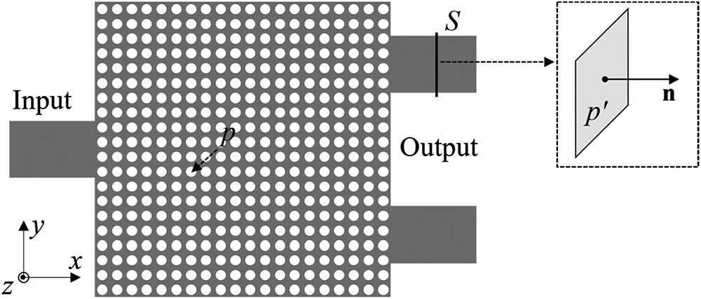
2. INVERSE DESIGN OF POWER DIVIDER
Figure 1.Schematic diagram of the single-mode 3 dB power divider (before optimization).
We define the figure-of-merit (FOM) of the device for inverse design as the transmission into the fundamental transverse electric mode () in the two output waveguides, and the transverse magnetic (TM) mode is neglected for simplicity. Because we keep all intermediate patterns axisymmetric, the FOM can be expressed as where is the cross section of the upper output waveguide, represents an arbitrary point in , and represent the electric and magnetic fields of the mode, and denote the actual electric and magnetic fields at , respectively. The overline means complex conjugation.
For a cylinder at position , a small change of its relative permittivity, , introduces an electric dipole moment, which leads to a variation of the electromagnetic field at . When we change the relative permittivities of all cylinders simultaneously, the total change of electric field at will be a superposition of variations caused by all cylinders. Based on the adjoint method for inverse design of analog patterns [1,5], the variation in FOM is given by where is the design region in all cylinders with the same and fixed shape, is the permittivity of vacuum, is the volume of a single cylinder, means the electric field at position before permittivity change, and represents the adjoint field at . Thus, the path to a gradient-based optimization could be reached by updating relative permittivity of each cylinder in iterations as to ensure that maintains positive; thus, device performance can be continuously optimized during the iteration process.
Figure 2.3 dB power divider. The optimized (a) analog and (b) quasi-digital patterns in the first and second stages, respectively. (c) The optimized ternary pattern in which the smaller air cylinders with a radius of 35 nm are highlighted in orange. (d) Simulated excess loss profiles for the three patterns. (e) Measured excess loss profiles and (f) the SEM image of the fabricated device based on the ternary pattern. Inset in (e) shows the simulated steady-state intensity distribution.
In the second stage, we convert the analog pattern in the first stage to a quasi-digital one in which the relative permittivities of most cylinders are close to 1 or 12. We use the same adjoint method to calculate the forward field and adjoint field but update the relative permittivities with a forced biasing in each iteration, expressed as Here, we set the variable to be 0.05 to slightly enlarge the distance between the relative permittivity and the central value 6.5, which may force the relative permittivity smaller than 1 or larger than 12; further, it will be clipped to be 1 or 12, respectively. This linear-biasing approach is an analogy similar to discrete optimization in the inverse design of analog nanophotonic devices [3], i.e., the inverse design region, which may help to ease the performance degradation caused by discretization of relative permittivities. We calculate the mean square error of the permittivity distribution () in each iteration as where is the number of cylinders, and is the relative permittivity of the th cylinder. The mean square error decreases significantly from 6.42 to 1.01 after 50 iterations, accompanied by a 0.002 dB increase of excess loss at 1550 nm. Figure 2(b) shows the optimized quasi-digital pattern in the second stage.
In the third stage, the quasi-digital pattern is transformed to an -ary digital pattern on the basis of effective medium theory. The basic idea is that cylinders with intermediate permittivities and an initial 45 nm radius in the quasi-digital pattern will be replaced with air cylinders with 45 nm radius, air cylinders with an appropriate radius smaller than 45 nm, or silicon cylinders. We use a ternary pattern () based on a three-level threshold for demonstration. The range of relative permittivity is divided into three segments with two intermediate values of 3.75 and 9.25. Cylinders with relative permittivities larger than 9.25 or smaller than 3.75 in the quasi-digital pattern will be simply filled with silicon or an air pattern, respectively. Meanwhile, cylinders with relative permittivities between 3.75 and 9.25 are replaced with smaller air cylinders based on a simple brute-force method. We decrease the radius of all smaller air cylinders from 44 to 30 nm with a step of 1 nm and then choose the value corresponding to the best FOM based on 15 rounds of 3D FDTD simulation results. Considering the fabrication constraint, the lower boundary value of the possible radius range is set to 30 nm. Here, the optimized smaller radius is 35 nm. In our simulation, the feature-size-dependent lag effect of RIE etching depth is always considered, and the etching depth of a cylinder with a radius of 35 nm is 124 nm [6]. Figure 2(c) shows the optimized ternary pattern in which the smaller air cylinders with a radius of 35 nm are highlighted in orange. Notably, if smaller quantization errors of intermediate relative permittivities are preferred, we can use the same method to obtain an -ary digital pattern with intermediate radii (smaller than the initial radius) for small air cylinders based on an -level threshold.
The simulated excess loss profiles of the analog, quasi-digital, and ternary patterns are given in Fig. 2(d). The average excess loss over 40 nm bandwidth (1530–1570 nm) is 0.32 dB for the analog pattern, and it increases slightly to 0.33 dB for the ternary digital pattern. The measured excess loss profiles and the scanning electron microscope (SEM) picture of the fabricated 3 dB power divider with the optimized ternary pattern are illustrated in Figs. 2(e) and 2(f), respectively. The measured average excess loss is 0.44 dB with a fluctuation up to 0.40 dB. The unbalance of excess loss between the two output waveguides is 0.36 dB at most and 0.14 dB on average.
3. INVERSE DESIGN OF THE DUAL-MODE DEMULTIPLEXER
Figure 3.Schematic diagram of the dual-mode demultiplexer (before optimization).
Here, two FOMs are used for inverse design. One () represents the transmission into the in the upper output waveguide when is input. The other () represents the transmission into the in the lower output waveguide when is input.
In the first stage of the digitized adjoint method, each iteration comprises four simulations for two FOMs. The forward and adjoint simulations for each FOM are similar to those in the optimization of a 3 dB power divider, and we first obtain the and based on the independent gradient-based optimizations of two FOMs, respectively. Then, we update the relative permittivity of each cylinder as Here, we set , and the convergence of the analog pattern optimization is reached after 100 iterations.
In the second and the last stages, we adopt the same methods used in inverse design of a 3 dB power divider to digitize the analog pattern. Specifically, we obtain the quasi-digital pattern of the dual-mode demultiplexer with after 100 iterations in the linear-biasing adjoint optimization based on Eq. (4). For the optimized ternary pattern, the radius of the small air cylinders is 36 nm.
Figure 4.Dual-mode demultiplexer. The optimized (a) analog and (b) quasi-digital patterns in the first and second stages, respectively. (c) The optimized ternary pattern in which the smaller air cylinders with a radius of 36 nm are highlighted in orange. (d) Simulated insertion loss and crosstalk profiles for the ternary pattern. Insets show the simulated steady-state intensity distributions of and modes, respectively. (e) and (f) Respectively, simulated and measured performance of a mode-division multiplexing system composed of a dual-mode multiplexer and a demultiplexer based on the ternary pattern. (g) and (h) Respectively, SEM images of the fabricated device based on the ternary pattern and the mode-division multiplexing system.
The computation times for the designs of the 3 dB power divider and dual-mode demultiplexer using the digitized adjoint method are about 1.2 and 7 h, respectively. For inverse designs of the two same devices using the conventional DBS method, the time spent on a single optimization process (convergence of the FOM) is approximately 5.5 to 36 h. Meanwhile, the simulated average excess losses over a 40 nm wavelength span (1530–1570 nm) of the 3 dB power dividers designed by the digitized adjoint method and DBS method are 0.33 dB and about 0.2 dB, respectively. For the dual-mode demultiplexer designed by the digitized adjoint method, the simulated insertion loss for both modes is 0.68 dB on average, and the crosstalk is from 1530 to 1570 nm, while such two parameters for the multiplexer designed by DBS method are 0.47 dB and less than from 1530 to 1590 nm, respectively. Compared with the brute-force DBS method, the proposed digitized adjoint method could improve the design efficiency by nearly five times, and the performance optimization can reach approximately the same level.
In conclusion, the digitized adjoint method is a hybrid of topology optimization and brute-force optimization to improve the efficiency of inverse design of high-performance digital subwavelength nanophotonic devices. Using the proposed method, we have designed and experimentally demonstrated a single-mode 3 dB power divider and a dual-mode demultiplexer with ternary digital patterns based on a PhC-like subwavelength structure, respectively. Compared with the DBS brute-force method, the digitized adjoint method increases the design efficiency by nearly five times while achieving approximately the same device performance. We expect that the digitized adjoint method can be used to design digital nanophotonic devices based on various types of subwavelength structures different from the PhC-like one. By breaking the efficiency bottleneck of the conventional brute-force method with computational time exponentially increased with the number of pixels and extending the conventional binary pattern to the multilevel pattern, the digitized adjoint method could be applied to the inverse design of large-scale digital subwavelength patterns for exploring digital nanophotonic devices with previously unattainable functionality or higher performance.