Single-photon detectors are ubiquitous devices in quantum-photonic-based communication, computation, metrology, and sensing. In these applications, -fold coincidence photon counting is often needed, for example, to characterize entanglement. However, -fold coincidence photon counting typically requires individual single-photon detectors and associated bias and readout electronics, and these resources could become prohibitive if goes large and the detectors need to work at cryogenic temperatures. Here, to break this limit on , we propose a device architecture based on cascaded photosensitive superconducting nanowires and one wider nanowire that functions as a current reservoir. We show that by strategically designing the device, the network of these superconducting nanowires can work in a synergic manner as an -photon detector, where can be from 1 to , depending on the bias conditions. We therefore name the devices of this type superconducting nanowire multi-photon detectors (SNMPDs). In addition to its simple one-port bias and readout circuitry, the coincidences are counted internally in the detector, eliminating the need for external multi-channel, time-correlated pulse counters. We believe that the SNMPDs proposed in this work could open avenues towards conveniently measuring high-order temporal correlations of light and characterizing multi-photon entanglement.
1. INTRODUCTION
Single-photon detectors are indispensable tools in quantum-photonic systems as well as in classical applications. Quantum-key distribution [1], linear optical quantum computation [2], photonic boson samplings [3–6], quantum metrology [7], Moon-to-Earth optical communications [8], and lidar [9] all need high-performance single-photon detectors. In particular, these detectors are often configured to measure coincidence of photons, for example, in Hong–Ou–Mandel [10,11] and Hanbury–Brown–Twiss interferometers [12,13]. Measuring -fold coincidence typically requires sets of single-photon detectors as well as the associated bias and readout electronics [11,13]; these resources could become prohibitive if goes large and if the detectors need to work at cryogenic temperatures. While individual superconducting nanowire single-photon detectors (SNSPDs) [14] have achieved unprecedented matrices of performance [15–20], it remains a challenge to scale single elements to large arrays to measure -fold coincidences, due, mainly, to the limitation of the cooling-power budget on the readout electronics accessing the detectors. Several multiplexing schemes, in time [10], frequency [21,22], amplitude [23–25], space [26,27], and row-column [28], have been proposed and demonstrated to simplify the otherwise formidably complicated readout circuits. However, it is still elusive whether it is possible to scale to a large number without resorting to a large number of electronic components.
In this paper, we propose a concept and a device architecture to achieve an -fold coincidence photon counter, in which can be set from 1 to by controlling the bias condition. The device is composed of photosensitive superconducting nanowires and one wider nanowire functioning as a current reservoir [29]. With its bias and readout circuitry as simple as one individual SNSPD, from the external point of view, the detector outputs a voltage pulse if and only if photons are detected. We therefore name the detectors of this type superconducting nanowire multi-photon detectors (SNMPDs).
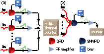
In Fig. 1, we contrast the commonly used technology for -fold coincidence photon counting with the proposed one using an SNMPD. As shown in Fig. 1(a), conventionally, in order to count -fold coincidence, individual single-photon detectors as well as the associated electronics are needed. After the detectors detect the photons, the multi-channel, time-correlated pulse counter counts the coincidences. In contrast, in this work, we propose to use a single SNMPD to count photons. For one -fold coincidence, the SNMPD directly outputs one voltage pulse. Thereby, we anticipate that the SNMPD could dramatically simplify the circuitry of the -fold coincidence counting.
Sign up for Photonics Research TOC. Get the latest issue of Photonics Research delivered right to you!Sign up now
Figure 1.Comparison between commonly used technology for -fold coincidence photon counting with the proposed one using a superconducting nanowire multi-photon detector (SNMPD) presented in this paper. (a) A conventional -fold coincidence photon counter requires single-photon detectors as well as the associated electronics. (b) We propose to use a single SNMPD to count -fold coincidence. SPD, single-photon detector; RF, radio frequency.
Figure 2 presents the device architecture of an SNMPD and its operating principle as an -photon detector. As shown in Fig. 2(a), the photosensitive nanowires () and the current reservoir () are all connected in parallel and then are connected with a choke inductor (with inductance of ) in series. We assume the photosensitive superconducting nanowires to be identical, although in principle they can be designed to be different. The set of parameters to characterize each of them includes kinetic inductance , switching current , and initial bias current . Accordingly, the kinetic inductance, switching current, and initial bias current of the current reservoir can be noted as , , and , respectively. The initial allocation of the total bias current to each branch is inversely proportional to the kinetic inductance of this branch, which explains the coefficient in .
Figure 2.Schematic drawing of the device layout and the operating principle of the SNMPDs. (a) Device layout. The SNMPD is composed of cascaded photosensitive superconducting nanowires () and a wider one functioning as a current reservoir (). See the main text for the definitions of , , , , , , , and . (b) Initial current distribution among the nanowires and the current reservoir. (c) Current redistribution after the first photosensitive nanowire is fired by the first photon. (d) Current redistribution after the th photosensitive nanowire is fired by the th photon. The current reservoir is also fired, and current is diverted into the load impedance . (e) The bias conditions for the device to work as an -photon detector as shown by the dashed lines. The open circles and triangles represent the upper bonds of , and the squares represent the lower bonds of . Note that the two sets of upper bounds (open circles and triangles) are identical.
Figures 2(b)–2(d) present the operating principle. Figure 2(b) shows the initial bias condition before any photon detection event occurs. As shown in Fig. 2(c), once the first photon is detected by the first photosensitive nanowire , which then temporarily switches to a high-impedance state, the current gets redistributed—the bias levels of the remaining photosensitive nanowires and the current reservoir all increase but do not exceed their corresponding switching currents. Similar procedures are repeated for the second, the third, …, and the ()th photons. When they are detected by the second, the third, …, and the ()th photosensitive nanowires, the bias level in the current reservoir increases in a staircase pattern. As shown in Fig. 2(d), when the th photon is detected by the th photosensitive nanowire , the redistribution of the current into the reservoir causes its switching to the high-impedance state, as the bias current exceeds its switching current . Most of the bias current in the reservoir then backflows to the photosensitive channels, causing all of them to switch to the high-impedance states. Therefore, the th photon functions as the “last straw” to switch the entire device. The bias current then flows through the load impedance , outputting a voltage pulse. The current subsequently restores in the photosensitive nanowires and the current reservoir after their superconductivity recovers. Note that this operating mode has no requirement on the sequence that the photons fire the photosensitive nanowires or on the time interval between two subsequent firings.
To operate the device in the -photon regime outlined above, we need to bias it in the correct bias conditions. These conditions can be summarized as the following. (i) After photosensitive nanowires have been fired by incident photons, the th photosensitive nanowire has not been switched to the normal state by current redistribution. (ii) After photosensitive nanowires have been fired by incident photons, the current reservoir has not been switched to the normal state by current redistribution. (iii) After photosensitive nanowires have all been fired by incident photons, the current reservoir will be switched to the normal state by current redistribution. These three conditions set constraints on the initial bias current ; specifically, conditions (i) and (ii) set the upper bounds, whereas (iii) sets the lower one. Appendix A details the derivations of these constraints. Two assumptions are important: one assumes that the inductance of the choke inductor is so large that each redistribution of the current does not cause leaky current to ; another assumes that the th photon-detection event on the th photosensitive nanowire, total amount of current , flows out from the photosensitive nanowire, where is a constant and is the bias current in the th nanowire prior to the th detection event. The first assumption can be realized experimentally to ensure the leaky current is negligibly small; the second assumption of to be a constant is an approximation, which has been justified by comparing the values of as a function of obtained by electrothermal simulations [30]. The justification is detailed in Appendix A. If we further design the device such that , the bias condition for the detector to work in the -photon regime is Specifically, electrothermal simulation shows that is approximately 0.8. The bias condition for each is calculated analytically and is presented in Fig. 2(e). The dashed lines present the bias regimes for the device to work as an -photon detector.
We present a simplest example, where , to quantitatively illustrate the electrothermal dynamics of the SNMPD. The bias condition is , fulfilling the requirement set by Eq. (1). The values of the parameters used in the electrothermal simulation are presented in Appendix B. Assume that at , the first photon is absorbed by the first photosensitive nanowire at the location , where is the direction along the nanowire. Figure 3(a) shows the electrothermal evolution of the device after the first photon is absorbed. The photon generates a resistive region around , but as the bias current is relatively low, the resistive region soon shrinks and disappears. The net effect is that the first photosensitive nanowire stabilizes in the superconducting state with an even decreased bias current , and the bias levels in the second photosensitive nanowire and the current reservoir become elevated to and , respectively, due to the redistribution of the current. However, as the bias currents are still less than their switching currents, both the second photosensitive nanowire and the current reservoir stay superconductive. Assume that the second incident photon is absorbed by the second photosensitive nanowire at and the location is noted as . Figure 3(b) presents the subsequent electrothermal evolution of the device. The second photon triggers a complete electrothermal evolution in the second photosensitive nanowire, in which the bias level has already been elevated by the previous current redistribution; furthermore, the redistribution of the current this time fires the current reservoir. The current in the reservoir backflows to the first and the second photosensitive nanowires, firing the first photosensitive nanowire even though is low. At this moment, the two photosensitive nanowires and the current reservoir all switch to high-impedance states, and the current flows through the load impedance , generating an output voltage pulse. Afterwards, the absorbed photon energy dissipates, the “hotspots” shrink and disappear, and the system recovers to its initial state. Therefore, it is the synergic effect of the first and the second photons that fires the entire detector—the first photon prepares for the avalanche by increasing the bias levels in the second photosensitive nanowire and the current reservoir, and the second photon initiates the avalanche. The current dynamics , , , and are presented in Fig. 3(c). We also present a video (Visualization 1) to visualize this complete electrothermal evolution.
Figure 3.Electrothermal dynamics of a superconducting nanowire two-photon detector. Panel (a) presents the electrothermal evolution after the first photon is absorbed by the first photosensitive nanowire at ; (a1), (a2), and (a3) present the current-temperature phase diagrams of the first and the second photosensitive nanowires and the current reservoir, respectively. Panel (b) presents the electrothermal evolution after the second photon is absorbed by the second photosensitive nanowire at ; (b1), (b2), and (b3) present the current-temperature phase diagrams of the first and second photosensitive nanowires and the current reservoir, respectively. In the phase diagrams, the open circles and solid dots present the initial and the final states, respectively, of the corresponding photon-detection event. The dotted lines in (a1) and (b2) represent the abrupt changes on the phase diagrams due to photon excitations, whereas the solid lines in (a1), (a2), (a3), (b1), (b2), and (b3) represent the continuous electrothermal evolutions of the nanowires after photon excitations. The black dashed lines separate the superconducting phase (S) and the normal phase (N) of the nanowires. The insets present the corresponding spatial-temporal diagrams of the temperature distribution. (c) Current dynamics of , , , and (see Visualization 1).
We now investigate how the device functions if the bias conditions given by Eq. (1) and shown in Fig. 2(e) are not satisfied. Apparently, if , even photons cannot fire the entire device to signal an output. On the other hand, if , we hypothesize that fewer photons are sufficient to fire the entire device so that it works as an -photon detector, where . Analysis on these more general cases shows the bias conditions for an -photon detector can be uniformly expressed as where . Figure 4 presents the bias conditions for different and in two different ways: Fig. 4(a)shows the bias regions with the maximum photon numbers for each (), with the second largest photon numbers for each (), and so on. Figure 4(b) shows the bias regions for a given photon number , for example, . We note that the data sets presented in Figs. 4(a) and 4(b) (the dots in these two subfigures) are identical; the difference is the lines for guiding the eyes and guiding the understanding of these data.
Figure 4.Bias conditions for the detector functioning as an -photon detector, where ; (a) and (b) present the same data set in two different ways. (a) The bias regions with the maximum photon numbers for each (), with the second largest photon numbers for each (), and so on. (b) The bias regions for a given photon number , for example, .
The role of the current reservoir is pivotal in our SNMPD, and it makes the device distinguished from SNSPDs and superconducting nanowire avalanche photodetectors (SNAPs). An SNSPD itself can work as a multi-photon detector [31,32], but in a low bias regime, and therefore the detection efficiency is low. So is that of an SNAP [33]. In contrast, the current reservoir allows us to engineer the bias condition, in particular, to boost the multi-photon regime to the high-bias region. Figure 5 presents the comparison of the bias conditions for multi-photon detection for an -SNAP and SNMPDs with two configurations. Compared with the -SNAP, the bias region for multi-photon detection is elevated in the SNMPD with and can further be elevated if we flexibly engineer the current reservoir; for example, let . See Eq. (A13) in Appendix A. Therefore, multi-photon detection with relatively high detection efficiency is the major advantage of SNMPDs integrated with current reservoirs.
Figure 5.Comparison within bias conditions for an -SNAP (black symbols), an SNMPD with (red symbols), and an SNMPD with (blue symbols).
To show the scalability of , we present our design of a superconducting nanowire eight-photon detector. As the electrothermal simulation becomes cumbersome when goes large, we used the SPICE-based model [34] as a simpler but equally effective tool to model the current dynamics. Each of the eight photosensitive superconducting nanowires is identical to the counterpart in the two-photon case, whereas the width of the current reservoir is increased to 400 nm and its kinetic inductance is decreased to 10 nH. The values of the parameters used in the SPICE simulation are presented in Appendix B. Figures 6(a)–6(c) show the current dynamics in the photosensitive nanowires, the current reservoir, and the output voltage pulse, respectively. Similar to what we have seen in the two-photon detector, the device outputs a voltage pulse if and only if the eight photons are respectively detected by the eight photosensitive nanowires. The limitation on is as presented in Fig. 2(e): when goes large, the appropriate bias regions shrink.
Figure 6.Current dynamics of a superconducting nanowire eight-photon detector. (a) Current dynamics of the eight photosensitive nanowires, (b) current dynamics of the reservoir, (c) the output voltage pulse on the load impedance without external amplification. The dashed lines in (a) and (b) present the switching currents.
By elevating the initial bias current, the eight-photon detector () can work in the -photon regime, where . For example, if we choose , the bias condition is , satisfying the requirement set by Eq. (2). Figure 7 presents the current dynamics of the eight-photon detector working in the six-photon regime.
Figure 7.Operation of a superconducting nanowire eight-photon detector in the six-photon regime. (a) Current dynamics of the eight photosensitive nanowires, (b) current dynamics of the reservoir, (c) the output voltage pulse on the load impedance without external amplification. The dashed lines in (a) and (b) present the switching currents.
Another advantage of SNMPDs is their simplicity. Their one-port bias and readout circuitry is as simple as the circuitry of one individual SNSPD. Furthermore, when an SNMPD works as an -fold coincidence counter, we can directly count the coincidences by counting the output voltage pulse, eliminating the need of external multi-channel pulse counters.
In addition to the scalability and the simplicity, it is also possible to configure an SNMPD to a photon-number-resolving detector. Very recently, researchers discovered that an SNSPD actually has intrinsic photon-number-resolving capability, but it is limited to the few-photon regime [35–37]. An interesting and distinct feature of SNMPDs is that prior to the “final fire” by the th photon, the information of the arrivals of the photons is essentially stored in the format of supercurrent in the current reservoir. For example, as shown in Fig. 6(b), the quantized step of the current increase per each photon is on the order of 3 μA, which can be readout by, for example, on-chip integrating yTron devices [38]. The successful readout of these steps of the current changes would also enable photon-number-resolving capability.
An alternative operating mode to resolving the photon number requires repetitive measurement. Assume that the incident light is in the -photon state and the photons are separated in spatial modes. To determine , we can repeatedly measure the light by configuring an SNMPD to be an -photon detector, ()-photon detector, …, and -photon detector that would only then output voltage pulses.
We evaluate the performance characteristics of the SNMPDs. The detection efficiency is determined by the product of the detection efficiencies of those photosensitive nanowires. The operating speed is set by , where is the total kinetic inductance, dominated by the inductance of the choke inductor , and is the load impedance. We expect that the accidentals, due to the false counts of the photosensitive nanowires, are negligibly low. The SNMPDs do not provide relative timing information among the photons unless the current reservoir is configured as the current-sensing mode introduced above so that the arrival time of each photon can be extracted.
If the detection scheme was extended to the photon-number-resolving scheme, the probability that an SNMPD with sections of photosensitive nanowires correctly measures the photon number in a weak optical pulse actually containing photons could be calculated by [39] , where DE is the detection efficiency of each photosensitive superconducting nanowire. For simplicity, the detection efficiency of the sections of photosensitive nanowires is assumed to be identical. The probability of error is therefore 1- . These calculations also assume, as in Ref. [39], that the weak optical pulse is originally in one spatial mode and is then split to couple with these photosensitive nanowires.
The SNMPDs do not have additional constraints on materials, optical structures, or fabrication processes, compared with SNSPDs. They allow both polycrystalline [14,40] and amorphous [15] materials commonly used for SNSPDs and allow both meander [40], spiral [41], and fractal [42,43] geometries for free-space coupling and hairpin structures for waveguide integration [44]. Integrating with waveguides naturally separates the photosensitive nanowires in space, and the waveguide integration may be convenient for coupling these photons that are already separated in different spatial modes, similar to what the authors of Refs. [27,45] presented. A schematic drawing of a waveguide-integrated SNMPD is presented in Appendix C. There is essentially no change in the fabrication processes used for making SNSPDs, except for that the device layout may become larger.
4. CONCLUSION
In conclusion, we have introduced the concept of SNMPDs. They are composed of photosensitive superconducting nanowires and one current reservoir, and they can be configured to -fold coincidence counters, where , by controlling the bias conditions. We have detailed the operating principle and have discussed their advantages, including simplicity in readout electronic circuitry and scalability. It is also possible to configure SNMPDs to photon-number-resolving detectors. The fabrication process for realizing SNMPDs is almost identical to that for SNSPDs. We anticipate realizing them experimentally as the next step and finding applications in measurement of high-order temporal correlations of light [13] and characterization of multi-photon entanglement [46].
APPENDIX A: BIAS CONDITIONS
To make the detector work correctly in the -photon regime, where , we need to bias it in appropriate bias regions. We now present the derivations of the bias conditions for the -photon regime.
Figures 2(b)–2(d) in the main text present the circuit model for the detector. We make the following assumptions to simplify the mathematics.
The kinetic inductance of each photosensitive nanowire is , which is assumed to be independent of the bias current; the kinetic inductance of the current reservoir is assumed to be , where is a coefficient.
The initial bias current in the th photosensitive nanowire is assumed to be . As are identical for , we note that . Therefore, the initial bias current in the current reservoir is .
The switching current of each nanowire is assumed to be , and the switching current of the current reservoir is denoted as , where is a coefficient.
The inductance of the choke inductor is assumed to be so large that each photon-induced current redistribution would cause negligible leaky current to the load impedance , unless all the nanowires and the current reservoir switch to the normal state with high impedance.
For the th photon-induced current redistribution as shown in Fig. 2(c), the current that flows out from the nanowire is , where is the bias current in the th photosensitive nanowire, prior to the th photon-detection event. For a given device architecture, we assume to be a constant. This assumption was justified by comparing as a function of , obtained by electrothermal simulation.
We first study the bias conditions for the case , in which the detector works as an -photon detector. The bias conditions for other cases, , can be obtained using a similar method.
To operate the device as an -photon detector, the following three conditions need to be satisfied.
After photosensitive nanowires have been fired by incident photons, the th photosensitive nanowire has not been switched to the normal state by current redistribution.
After photosensitive nanowires have been fired by incident photons, the current reservoir has not been switched to the normal state by current redistribution.
After photosensitive nanowires have all been fired by incident photons, the current reservoir will be switched to the normal state by current redistribution.
We translate these three conditions to the constraints on .
Condition (i)
After the first photosensitive nanowire is fired, total amount of current redistributes in the remaining photosensitive nanowires and the current reservoir. The increase of the current in each nanowire is inversely proportional to the kinetic inductance of each nanowire and the current reservoir. Therefore, the increase of the bias current in each of the remaining photosensitive nanowires, due to the redistribution of the current, is where . Therefore, the bias current in each of the photosensitive nanowires becomes where .
After the second photosensitive nanowire is fired by the second photon, the redistribution of the current leads to the increase of bias current in each photosensitive nanowire. and can be calculated by and respectively, where .
After the ()th photosensitive nanowire is fired by the ()th photon, the bias current in the th photosensitive nanowire becomes Condition (i) says that should be less than in order to maintain the superconductivity of the th photosensitive nanowire: or, equivalently, Condition (ii)
After the ()th photosensitive nanowire is fired by the ()th photon, the bias current in the reservoir is Condition (ii) says that should be less than in order to maintain the superconductivity of the current reservoir: or, equivalently, Condition (iii)
After the th photosensitive nanowire is fired by the th photon, the bias current in the current reservoir becomes Condition (iii) says that should be larger than the switching current of the current reservoir to ensure its switching: Eqs. (A7), (A10), and (A12) set constraints on , and they can be further simplified.
We assume , which means that the initial bias currents in the photosensitive nanowires and the current reservoir, normalized to the corresponding switching currents, are identical. Consequently, Conditions (i) and (ii) become equivalent. Therefore, the bias condition is We further assume , and the bias condition for the detector to work as an -photon detector is Specifically, electrothermal simulation shows that is approximately 0.8 for our designed device. The bias condition for the detector is , as a function of , is plotted in Fig. 2(e) in the main text.
For the general cases in which the detector works as an -photon detector, where , the bias conditions can be obtained by replacing the exponential with in Eqs. (A13)–(A15). Figure 4 in the main text presents the bias conditions for the detector to work in the -photon regime.
To justify assumption (5), we use the superconducting nanowire two-photon detector discussed in the main text as an example. We simulated as a function of using electrothermal simulation [30]. Figure 8 presents the results. For the first photon is slightly below 0.8, whereas for the second one is slightly above 0.8. Therefore, using the constant value of 0.8 is a valid approximation.
Figure 8. as a function of , obtained by electrothermal simulation, for a superconducting nanowire two-photon detector. For the first photon, is slightly below 0.8; for the second photon, is slightly above 0.8.
APPENDIX B: PARAMETERS AND THEIR VALUES USED IN SIMULATIONS
The parameters and their values used in the electrothermal simulations are listed in Table 1; the values of other material parameters, not listed in Table 1, are identical with those used in Ref. [30]. The parameters and their values used in the SPICE simulations are listed in Table 2.
APPENDIX C: WAVEGUIDE-INTEGRATED SNMPDS
Figure 10 presents the schematic drawing of a waveguide-integrated SNMPD. Photons are separated in spatial modes, which are coupled, confined, and guided by integrated waveguides on chip. Then photons are detected by photosensitive nanowires , which are coupled with the waveguides.
[9] G. G. Taylor, D. Morozov, N. R. Gemmell, K. Erotokritou, R. H. Hadfield. 2.3 μm wavelength single photon lidar with superconducting nanowire detectors. CLEO: Science and Innovations, JTh2A–93(2019).
[29] Y. Cheng, H. Liu, C. Gu, X. Zhu, X. Hu. Superconducting nanowire single-photon detectors integrated with current reservoirs. CLEO: Science and Innovations, JW2A–120(2017).
[37] D. Zhu, M. Colangelo, C. Chen, B. A. Korzh, F. N. Wong, M. D. Shaw, K. K. Berggren. Resolving photon numbers using a superconducting tapered nanowire detector(2019).