Bowen Sheng1,2, Gordon Schmidt1,6,*, Frank Bertram1, Peter Veit1..., Yixin Wang2, Tao Wang2, Xin Rong2, Zhaoying Chen2, Ping Wang2, Jürgen Bläsing1, Hideto Miyake3, Hongwei Li4, Shiping Guo4, Zhixin Qin2, André Strittmatter1, Bo Shen2,5, Jürgen Christen1 and Xinqiang Wang2,5,7,*|Show fewer author(s)
1Institute of Physics, Otto-von-Guericke-University Magdeburg, 39106 Magdeburg, Germany
2State Key Laboratory for Mesoscopic Physics and Frontiers Science Center for Nano-optoelectronics, School of Physics, Peking University, Beijing 100871, China
3Department of Electrical and Electronic Engineering, Mie University, Mie 514-8507, Japan
4Advanced Micro-Fabrication Equipment Inc., Shanghai 201201, China
5Collaborative Innovation Center of Quantum Matter, Peking University, Beijing 100871, China
Investigating closely stacked GaN/AlN multiple quantum wells (MQWs) by means of cathodoluminescence spectroscopy directly performed in a scanning transmission electron microscope, we have reached an ultimate spatial resolution of . The pseudomorphically grown MQWs with high interface quality emit in the deep ultraviolet spectral range. Demonstrating the capability of resolving the 10.8 nm separated, ultra-thin quantum wells, a cathodoluminescence profile was taken across individual ones. Applying a diffusion model of excitons generated by a Gaussian-broadened electron probe, the spatial resolution of cathodoluminescence down to the free exciton Bohr radius scale has been determined.
1. INTRODUCTION
Quantum heterostructures, like quantum wells (QWs) [1–3], wires [4–6], disks [7–9], or dots [10,11], are key elements for the development of future nanophotonic semiconductor devices. These quantum objects change their optical and electronic properties drastically with slight variation of their spatial dimensions, chemical composition, or crystal strain. The combination of electron microscopy and cathodoluminescence (CL) spectroscopy directly enables the correlation of real structure and luminescence/electronic states of individual quantum structures at once [12–21]. Therefore, the primary challenge in CL microscopy is the improvement of the spatial resolution down to the scale of quantum heterostructures to distinguish and probe them individually or even their innermost part.
2. EXPERIMENTAL METHODS
Performing CL microscopy directly in a scanning transmission electron microscope (STEM-CL), we demonstrate the capability of resolving individual GaN QWs down to the free exciton Bohr radius scale in this paper. Despite our global light collection scheme leading to diffusion-broadened CL distribution, we are able to clearly identify single QWs, which are closely stacked in GaN/AlN multiple quantum wells (MQWs). The unintentionally doped 100-fold MQW structure is grown by metal-organic vapor phase epitaxy (MOVPE) in an AMEC Prismo high temperature reactor on a high-quality thermally annealed AlN/sapphire template. The nominal monolayer-thin GaN films grown at 1050°C are separated by 10 nm thick AlN barriers. A detailed description of the MOVPE growth can be found elsewhere [22].
The room-temperature (RT) STEM-CL investigations were performed at 80 kV acceleration voltage in a (S)TEM Tecnai F20 equipped with a parabolically shaped mirror and monochromator system MonoCL4. Detailed information about our STEM-CL setup has been reported previously [23,24]. The atomic structure of the QWs has been analyzed by high-resolution STEM (HRSTEM) at 300 kV in an FEI Titan Cubed Themis G2. For STEM-CL as well as HRSTEM, cross-section specimens were prepared by conventional mechanical polishing followed by + ion milling. The crystal quality of the GaN/AlN MQWs was characterized by high-resolution X-ray diffraction (XRD) measurements in a Bruker D8 system. XRD diffractograms were simulated with the software Leptos from Bruker.
Sign up for Photonics Research TOC. Get the latest issue of Photonics Research delivered right to you!Sign up now
3. RESULTS AND DISCUSSION
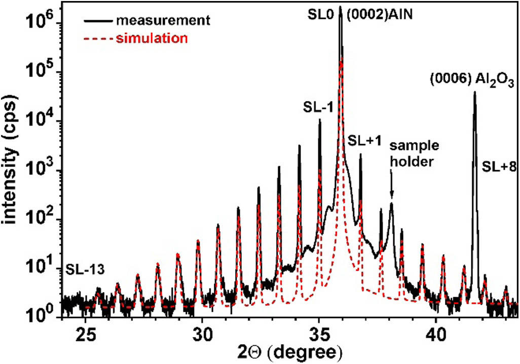
Figure 1 displays the XRD scan along the (0002) direction. Overlapping with the AlN (0002) diffraction peak, the MQW peak is located at 36° and indicates a pseudomorphic growth of the GaN MQWs on the AlN buffer. Satellite peaks up to the 13th order were observed due to constructive interference of X rays reflected at the MQWs’ interfaces, which implies a coherent periodicity of the GaN/AlN heterostructure and the presence of sharp interfaces. The slight asymmetric line shape of the satellite peaks, in particular clearly seen for high-order peaks, is caused by an asymmetric distribution of the period thickness of QW and barrier. Including these asymmetric thickness variations, the simulation of the XRD pattern (red dashed line in Fig. 1) is in good agreement with the experimental data. Consequently, an average period thickness of with variations of 0.35 nm was determined.
Figure 1.High-resolution XRD pattern of scan of GaN/AlN MQWs along the (0002) direction (black curve) with well-matched simulation (red dashed line) considering asymmetric thickness deviations.
The STEM high-angle annular dark field (HAADF) image [Fig. 2(a)] clearly shows the periodic structure of the GaN/AlN MQWs with a thickness of 1.08 μm in total. The threading dislocation density is in the range of . Under higher magnification [see Figs. 2(b) and 2(c)], the STEM-HAADF contrast exhibits the embedded GaN quantum wells (bright contrast) in the AlN matrix (dark contrast). A modest interdiffusion can be seen in the STEM images, which might be caused by the relatively high growth temperature in MOVPE [22] leading to a different interface quality near the buffer in comparison to the upper part of the QW stack. The interdiffusion of Ga is more pronounced at the bottom of the stack than at the top [Figs. 2(b) and 2(c)]. In general, the lower interface is sharper than the upper one for each single GaN QW. Additionally, no misfit dislocations are observed at the interfaces. The period thickness of the MQWs is about . Within the error bar, the measured thicknesses derived from local TEM analysis and spatially averaged XRD are consistent.
Figure 2.(a) STEM-HAADF image in cross-section view shows well-defined periodic structure of GaN/AlN MQWs grown on AlN buffer layer. High-resolution STEM-HAADF images taken from the (b) top and (c) bottom parts of a GaN QW stack indicate sharp interfaces. The bright (dark) contrast corresponds to GaN (AlN).
Room-temperature STEM-CL measurements were performed at specimen thicknesses of , making a compromise between CL signal-to-noise ratio and spatial resolution. The local STEM-CL spectra of the GaN/AlN MQWs (red spectrum) as well as the AlN layer (blue spectrum) integrated over the cross section are shown in Fig. 3. The main peak at 232 nm (5.343 eV) is assigned to the GaN/AlN MQWs’ emission with a full width at half-maximum (FWHM) of about 295 meV (). Reports about theoretical optical transition energies of GaN/AlN QWs give rise to effective QW thicknesses monolayers (MLs) for our observed emission energies [25–27]. However, abrupt interfaces are accounted for in these calculations, which are not observed in our MQW structure. Despite nominal GaN growth, unintentional incorporation of residual Al cannot be completely excluded due to interdiffusion shown in Figs. 2(b) and 2(c) leading to an increase of the QW fundamental band gap. Nevertheless, effective QW thickness of MLs is assumed because of the high exciton binding energies in these structures. The large spectral broadening of the MQWs’ emission might be caused by interface roughness as already seen in the STEM images presented here [28,29]. There is no near band edge luminescence from the AlN barriers, while only a broad emission from AlN-related oxygen deep donor levels (DX centers) can be found at around 400 nm [30], mostly originating from the AlN layer.
Figure 3.STEM-CL local spectra of the GaN/AlN MQWs (filled red spectrum) and of the AlN layer (blue spectrum) taken at room temperature (RT) in the cross section of the sample. The main peak at 232 nm is assigned to the GaN/AlN MQWs with a weak and broad AlN luminescence from related oxygen DX centers found around 400 nm.
The STEM-HAADF image [Fig. 4(a)] with the corresponding panchromatic CL intensity image [Fig. 4(b)] resolves the first 13 QWs just above the AlN buffer layer. The QWs show intense, uniform deep UV emission. Whereas the HAADF signal clearly shows a distinct contrast between AlN and GaN layers, there are only slight variations in CL intensity. Nevertheless, a noticeable intensity increase exists at every QW position: the panchromatic CL intensity increases from the AlN barrier towards the QW and subsequently decreases towards the following AlN barrier. To clearly visualize and evaluate the intensity modulation, profiles of HAADF signal and panchromatic CL intensity are displayed in Figs. 5(a) and 5(b), respectively. Both profiles were laterally integrated over a width of 50 nm. From the profiles, the precise correlation between the structural and optical properties is given. The HAADF signal shows a well-defined periodic Gaussian-shaped modulation of the MQWs, giving the position of the GaN layer at its maxima. The period length can be easily extracted from the profile as , which is in good agreement with XRD and HRSTEM results. The width of the profile is , providing the Gaussian beam broadening of the ML-thick GaN films in HAADF averaged over the whole specimen thickness. Due to the small QW thickness compared to broadening, the differences between the generalized error function resulting from convolution of a Gaussian beam with a rectangular material profile and the Gaussian function are negligible. Hence, we are using the latter one for determining .
Figure 4.(a) STEM-HAADF image of the first 13 GaN/AlN QWs with corresponding (b) panchromatic CL intensity image measured at RT.
Figure 5.(a) Profiles of HAADF signal and (b) CL intensity (blue bar graph) with fit function (red curve), corresponding to the solution of the one-dimensional exciton diffusion model in an MQW, yielding a spatial resolution of and a diffusion length of .
Since CL originates from the inelastic interaction of matter with accelerated electrons, the CL resolution is determined first by the interaction volume within the solid. In scanning transmission electron microscopy applied to thin electron transparent prepared foils, the interaction volume is described in good approximation by the mathematical convolution of the initial electron probe size and the beam broadening, which occurs as the primary electrons traverse the specimen. For modern STEM, the electron probe is extremely small (with diameter ) and is affected by the given parameters of the specific electron microscope. The beam probe profile can be approximated by a Gaussian-like distribution with the standard deviation . Focused on the TEM foil, the primary electrons are scattered and produce a spatial distribution that broadens the incident electron probe normal to the beam direction known as beam broadening. A widely known definition of beam broadening is derived from the single scattering model by Goldstein et al. [31], where the effective beam broadening is defined as the diameter of the exit foil surface including 90% of the Rutherford scattered electrons. For high-energy electron beams and Gaussian electron distribution at the exit surface, the formula from Reimer is used here [32], which is, except for the relativistic correction, identical to Ref. [31]. In terms of statistical consistency, the beam broadening is described by the standard deviation : with the mass density, the relative atomic mass, the atomic number, the electron energy, the electron rest energy, and the foil thickness. Thus, we obtain an overall STEM resolution .
The probes for luminescence experiments on semiconductors are electron–hole pairs, which are generated by the inelastic scattering process of the primary electron beam. For low-temperature (liquid He) as well as room-temperature experiments on many non-degenerated wide-band-gap semiconductors, like III-nitrides, the electron–hole pairs form Coulomb-bound excitons with diameter up to several crystal unit cells. Accordingly, the principal physical limit for the spatial resolution in CL investigations on these kinds of materials is the volume of these free excitons. Hence, to obtain the total generation volume in CL, the interaction volume has to be convoluted with the volume of the free exciton. In the effective-mass theory, Wannier–Mott excitons in the 1s state exhibit a standard deviation of the spatial probability density of with the exciton Bohr radius [33]. Consequently, the CL generation function for Gaussian electron beam excitation is defining the CL spatial resolution.
By choosing proper STEM parameters, falls even below in group III-V semiconductors. Higher acceleration voltages lead to a smaller beam broadening and therefore smaller interaction volume; however, at the same time they result in a drastic increase of sample damage during the electron beam exposure leading to quenching of CL intensity. Choosing 80 keV electrons, the sample damage is only minor [34], and the electron beam is broadened by in a 100 nm thick AlN layer, which is close to of the free exciton. Depending on the various reported permittivities and effective masses for AlN, can be estimated as 1.06 nm [35,36]. The resulting extremely high spatial resolution in the range of 1–2 nm is hardly reachable with any other far-field diffraction-limited optical techniques, like “standard” SEM-CL [37] or micro-photoluminescence [38], or even a scanning near-field optical microscope (SNOM) [39,40].
In the far-field detection scheme, where the generated carriers are locally excited and the luminescence is globally collected and detected, the CL spatial distribution is further determined by the transport of the generated carriers. In the case of excitons, the transport is generally described by classical diffusion caused by the concentration gradient and without drift components due to the electrical neutrality of the excitons. Along the growth direction for a QW at position embedded between thick barriers, the one-dimensional diffusion differential equation is solved by assuming a Gaussian generation function [Eq. (2)] and with the exciton diffusion length, the exciton concentration, and erfc{ } the complementary error function. The diffusion length depends on the transport properties of carriers in the sample influenced by the material, alloy disorder, interfaces, and doping, and it can be influenced by measurement parameters such as sample temperature or excitation density. In general, is equal to with the diffusivity and the exciton lifetime. In a thin foil, the crystal surfaces adjacent to the generated carriers will have a critical effect on the diffusion length due to surface recombination, which results in decreased as compared to bulk [40]. While typical bulk diffusion lengths for minority carriers in group III–V semiconductors at room temperature (RT) are 100 nm (GaN) [41] and μ (GaAs) [42], much smaller diffusion lengths result in the thin TEM foil.
The CL variation is shown in Fig. 5(b), where the CL intensity is spatially modulated slightly between 95% and 100%. However, the periodic modulation originating from the sequence of the individual QWs of the MQW stack is clearly observed and matches perfectly with the QW HAADF contrast. The period thickness of agrees with those determined by XRD and STEM. As expected, the intensity maximum is observed when the electron beam hits the very center of the monolayer-thick QW. According to the one-dimensional diffusion model for excitons, we are using the superposition of Eq. (3) as the fit function [red curve in Fig. 5(b)]. Excitonic transport is reasonable due to the large exciton binding energies in these structures [43,44]. The fitting agrees perfectly well with our experimental data and yields a standard deviation of and a diffusion length of . In this context, the CL profile can be understood in the sense of the high CL spatial resolution and the diffusion, while the former leads to the spatial modulation and the latter causes the high offset with reduced intensity contrast. In the MQW, the individual QWs are closely stacked such that the CL intensity profiles of adjacent QWs overlap, resulting in a small intensity variation.
The remarkable CL resolution of 1.8 nm is according to Eq. (2) a function of the STEM interaction volume and the exciton extent. In QW heterostructures of finite barrier height, the exciton wave function leaks into the barriers. As a consequence, the exciton Bohr radius decreases with decreasing QW width due to confinement and then increases back towards the bulk barrier exciton Bohr radius. In the limit of ultrathin GaN QWs, the QW exciton Bohr radius is very close to its AlN bulk value. Here, 88 nm effective foil thickness is in a reasonable range for STEM-CL investigations from experience and was calculated corresponding to and .
The CL resolution as well as the interaction extent is even smaller than , which is a consequence of the different scattering processes leading to HAADF and CL signal. The quasi-elastic thermal diffuse scattering at the partially screened atomic cores is known for the contrast formation in HAADF, whereas the primary electrons have to be scattered inelastically at valence electrons for electron–hole pair generation. Both scattering volumes do not have to be identical in general. In particular, inelastic scattering occurs statistically by exceeding its mean free path in contrast to thermal diffuse scattering.
The thin-film preparation, in terms of surface recombination and introducing non-radiative recombination sites, is assumed to affect the exciton diffusion lengths in STEM-CL. For this reason, the determined diffusion length is a specific value for our investigations and might be different from a non-prepared sample. For undoped AlN, we reported low-temperature diffusion lengths up to 113 nm in STEM-CL experiments on TEM prepared samples [45]. Reports about diffusion lengths in AlN in non-prepared samples are rare. Only Lopatiuk-Tirpak et al. determined a minority carrier diffusion length of in a Mg-doped short-period superlattice [46].
Despite several STEM-CL publications, only a few quantitative statements about the spatial resolution in STEM-CL are found in the literature [19,47–50]. Zagonel et al. reported the resolution of 4 nm separated optical features in nanowires with embedded InGaN quantum disks [19]. However, a physical model and theoretical analysis of the data in terms of taking diffusion, exciton Bohr radius, as well as STEM resolution into account is completely missing. In general, the probe size of the quasi-particle generated in the material, which is in our case the exciton, is the principal physical limiting factor of spatial resolution in any luminescence experiment and has to be considered for highly spatially resolved CL analysis. Even for thinner samples, higher acceleration voltages, or aberration-corrected microscopes, which all result in a higher STEM resolution, the exciton still spatially averages over its 1s wave function and exhibits luminescence across its volume.
4. SUMMARY
In summary, we demonstrated the capability of resolving single closely separated QWs embedded in GaN/AlN MQWs in CL down to the free exciton Bohr radius scale. The overall 10.85 nm period thickness of the pseudomorphically grown MQWs was determined by STEM-CL and was verified by XRD as well as locally by HRSTEM. In cross-sectional STEM-CL, the MQWs emit in the deep UV range at 232 nm. CL intensity profiles across individual GaN QWs show a modulation with the highest intensity at the QW position. This demonstrates the high spatial resolution of our STEM-CL setup, whereas the small modulation amplitude is attributed to diffusion-broadened CL distribution. Applying a diffusion model of excitons generated by a Gaussian-broadened beam, we were able to determine the remarkable CL spatial resolution of 1.8 nm, which is close to the physical resolution limit given by the exciton diameter.
Acknowledgment
Acknowledgment. Many thanks to Silke Petzold for her work regarding the specimen preparation.
[31] J. I. Goldstein, O. Johari, J. L. Costley, G. W. Lorimer, R. J. B. Reed. Quantitative X-ray analysis in the electron microscope. Scanning Electron Microscopy(1977).
[32] L. Reimer, H. Kohl. Transmission Electron Microscopy: Physics of Image Formation, 36(2008).
[33] J. O. Dimmock, R. K. Willardson, A. C. Beer. Introduction to the theory of exciton states in semiconductors. Semiconductors and Semimetals, Volume 3, Optical Properties of III-V Compounds(1967).