Abstract
We report on the performance of AlGaN-based deep ultraviolet light-emitting diodes (UV-LEDs) emitting at 265 nm grown on stripe-patterned high-temperature annealed (HTA) epitaxially laterally overgrown (ELO) aluminium nitride (AlN)/sapphire templates. For this purpose, the structural and electro-optical properties of ultraviolet-c light-emitting diodes (UVC-LEDs) on as-grown and on HTA planar AlN/sapphire as well as ELO AlN/sapphire with and without HTA are investigated and compared. Cathodoluminescence measurements reveal dark spot densities of , , , and in multiple quantum well samples on as-grown planar AlN/sapphire, HTA planar AlN/sapphire, ELO AlN/sapphire, and HTA ELO AlN/sapphire, respectively, and are consistent with the threading dislocation densities determined by transmission electron microscopy (TEM) and high-resolution X-ray diffraction rocking curve. The UVC-LED performance improves with the reduction of the threading dislocation densities (TDDs). The output powers (measured on-wafer in cw operation at 20 mA) of the UV-LEDs emitting at 265 nm were 0.03 mW (planar AlN/sapphire), 0.8 mW (planar HTA AlN/sapphire), 0.9 mW (ELO AlN/sapphire), and 1.1 mW (HTA ELO AlN/sapphire), respectively. Furthermore, Monte Carlo ray-tracing simulations showed a 15% increase in light-extraction efficiency due to the voids formed in the ELO process. These results demonstrate that HTA ELO AlN/sapphire templates provide a viable approach to increase the efficiency of UV-LEDs, improving both the internal quantum efficiency and the light-extraction efficiency.1. INTRODUCTION
AlGaN-based ultraviolet-c light-emitting diodes (UVC-LEDs) with an emission wavelength below 280 nm are suited to applications such as water disinfection, biochemical agent detection, and gas sensing [1–3]. However, the external quantum efficiency (EQE) of UVC-LEDs is still modest compared with that of LEDs emitting in the visible spectral range [3,4]. With its UV transparency as well as its low cost, sapphire substrates are commonly used for UV-LEDs. One limiting factor is the large lattice mismatch between aluminium nitride (AlN) and sapphire [5], typically resulting in threading dislocation densities (TDDs) in the range of [6]. To realize UV-LEDs with a high internal quantum efficiency (IQE), dislocation densities below are necessary [3,7]. In the past years, several publications have demonstrated the beneficial effect of high-temperature annealed (HTA) process on the crystal quality of AlN layers on sapphire, resulting in TDD below mainly by eliminating the twist components between the buffer layer grains [8,9]. A different technique successfully applied for dislocation reduction is the epitaxial lateral overgrowth (ELO) of patterned sapphire substrates [6,10]. Additionally, using patterned sapphire substrates, an increase in light extraction efficiency (LEE) is expected by reducing the loss of light by total reflection at the AlN–sapphire interface and subsequent absorption in the quantum wells (QWs) and at the contacts [11–14]. In this paper, we report on the combined beneficial effects of HTA process and of a patterned AlN–sapphire interface on the crystal quality and the performance characteristics of AlGaN-based UVC-LEDs emitting at 265 nm. We will compare and investigate UVC-LEDs grown on as-grown planar AlN/sapphire and on HTA planar AlN/sapphire as well as ELO AlN/sapphire with and without HTA process.
2. EXPERIMENT
All templates were grown on (0001) c-plane sapphire substrates [15]. Thermal in situ cleaning of the sapphire substrates was performed by an annealing step at 1150°C in hydrogen ambient. The AlN starting layers were grown at susceptor temperatures of 1350°C, measured by in situ pyrometry. Planar templates were fabricated by growing 1.5 μm AlN on (0001) sapphire substrates [15]. The planar HTA templates are based on 0.9 μm metal organic chemical vapor phase epitaxy (MOVPE) grown AlN layers. These layers were then face-to-face annealed at 1700°C in nitrogen ambient as described in Ref. [16]. ELO templates were fabricated by first growing 0.5 μm AlN on planar sapphire. Subsequently, these layers were patterned into stripes by photolithography and dry-etching steps and overgrown by MOVPE with a 5 μm thick AlN layer [17]. The HTA ELO templates were fabricated similar to the ELO template. However, the first 0.5 μm AlN layer was face-to-face annealed at 1700°C in nitrogen ambient before patterning to reduce the TDD in the AlN seed layer on the etched stripes.
AlGaN-based LED heterostructures with an emission wavelength of 265 nm were grown simultaneously onto these different AlN templates using a close-coupled showerhead MOVPE system. A 600 nm thick homoepitaxial AlN buffer layer and a 25 nm thick transition layer from AlN to is followed by the side. The side consists of a 900 nm thick current spreader, a 100 nm thick AlGaN:Si transition layer, and a 200 nm thick contact layer [18]. The active zone contains a threefold multiple quantum well (MQW) followed by a 10 nm thick electron blocking layer (EBL), allowing for an emission wavelength of 265 nm [19,20], a 25 nm thick Mg-doped EBL, and a 200 nm thick GaN:Mg contact layer. For the on-wafer measurements, UVC-LEDs were processed from the different wafers using palladium-based contacts and vanadium-based contacts [21].
Sign up for Photonics Research TOC. Get the latest issue of Photonics Research delivered right to you!Sign up now
High-resolution X-ray diffraction rocking curve (HRXRD-RC, open-detector) measurements were performed to estimate the TDD of the AlN/sapphire templates. Plane-view panchromatic cathodoluminescence (CL) measurements were carried out at low temperature (80 K, 5 kV) on AlGaN MQW samples with a heterostructure identical to the UVC-LEDs except for the omitted p-layers. Furthermore, cross-section transmission electron microscopy (TEM) imaging on MQW samples under different diffraction conditions was performed. The output power and voltage characteristics of the UVC-LEDs were measured on-wafer in a bottom-emission configuration using a calibrated large-area silicon photodiode and a compact UV-VIS StellarNeT EPP 2000 spectrometer. The on-wafer LEE of the UVC-LED devices was estimated by Monte Carlo ray-tracing simulations [14]. Furthermore, flip-chip bonding was carried out to mount the UVC-LED chips on an AlN-based planar package. Pt-based electrodes were used for the contacts, and the output powers were measured in a calibrated integrating sphere and at a controlled temperature of 288 K. In addition, a silicone-based material, with a refractive index of 1.45 and an absorption coefficient less than at the LED emission wavelength, was used for the encapsulation of the high-efficiency UVC-LED chips.
3. RESULTS AND DISCUSSIONS
Prior to the AlGaN growth, the rocking curve full width at half maximum (RC-FWHM) of the symmetric (0002) and the skew-symmetric () or () AlN reflection of the AlN/sapphire templates was determined. Note that, for the ELO templates, the () was used to reduce the broadening of the AlN reflection by wing tilt due to the stripe pattern. The estimated TDDs from the RC-FWHM [22] are for the planar, for the HTA planar, for the ELO, and for the HTA ELO templates. It is worth mentioning that, due to the large X-ray spot size, the estimated TDDs of the ELO templates include both the reduced TDD region above the ELO trenches and the region above the ELO ridges with higher TDD. Hence, an improved crystal quality of the AlN layer on the planar as well as on the stripe-patterned sapphire substrate is achieved by HTA treatment.
After 400 nm, AlN overgrowth of the different AlN/sapphire template surfaces with bilayer steps with a step height of c/2 is achieved for all templates. Figure 1 shows atomic force microscopy (AFM) images of the surface of the MQW samples on the different AlN/sapphire templates. The AFM images reveal a spiral-growth-dominated morphology, which develops during AlGaN overgrowth, in contrast with the step flow growth that is observed on the surfaces of the AlN/sapphire templates. Similar surface morphologies were reported [23–25]. The MQWs have similar surfaces with roughly the same hillock density of . However, the MQW sample on top of the HTA ELO template shows a reduced hillock density of caused by a lower screw dislocation density.
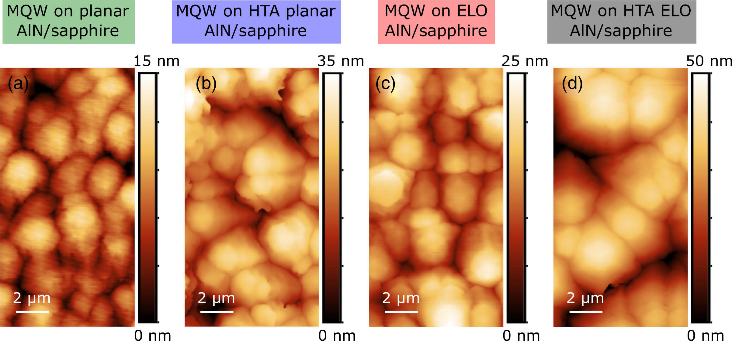
Figure 1.AFM images of the MQW samples on (a) planar, (b) HTA planar, (c) ELO, and (d) HTA ELO templates.
The TDDs of the AlGaN-based MQWs on the different templates were estimated by plane-view CL performed at 80 K, as nonradiative recombination occurring at the TDs causes dark spots in the CL image (Fig. 2). The MQW samples exhibit a dark spot density (DSD) of (planar), (HTA planar), (ELO), and (HTA ELO). These values reveal the same trend as the TDDs estimated by HRXRD. The dark spots are distributed evenly for all samples except for the MQW on the ELO template, which shows regions of higher and lower dark spot density [25] caused by a variation of TDD induced by the patterned ELO process, whereas it cannot be clearly identified on the HTA ELO template. This is most likely attributed to the already low TDD of the HTA layer before overgrowth, which reduces the DSD contrast between the regions above the ELO trenches and ridges.

Figure 2.Panchromatic CL topograms at 80 K of the MQW samples on (a) planar, (b) HTA planar, (c) ELO, and (d) HTA ELO templates.
To analyze the microstructure of the MQW samples, cross-sectional TEM diffraction contrast images of the MQW samples on HTA planar, ELO, and HTA ELO templates were selected. Figure 3 shows the cross-sectional TEM images recorded under two different and orthogonal two-beam diffraction conditions with and , respectively. Due to the different contrast of the same TD-type in the two cases (proportional to , where is the Burgers vector of the associated dislocation), TDs with a c-component in their Burgers vector (usually screw-type with or with mixed screw/edge character) are observable with , and TDs with an a-component in their Burgers vector (usually edge-type with or mixed) are observable with . First, the ELO growth is similar with and without HTA treatment and forms nearly identical ELO voids, i.e., the same effect on the LEE is expected. The TDD is significantly reduced above the ELO trenches, and a further TDD reduction occurs by dislocation annihilation with increasing AlN thickness. The average total TDD of the MQW samples on HTA planar, ELO, and HTA ELO templates is determined to be , , and , respectively. Since the screw- and mixed-dislocation densities are about one order of magnitude lower than the edge dislocation densities, a further reduction in the screw dislocation densities approaches the TEM detection limit, leading to unreliable statistics. However, Fig. 3(d) indicates a higher screw- and mixed-type dislocation density compared with the HTA-based templates.
Figure 3.Cross-sectional TEM images of the MQW samples on (a) and (b) HTA planar, (c) and (d) ELO, and (e) and (f) HTA ELO templates under different diffraction contrast conditions ( vector displayed in each image).
Figure 4(a) shows the current-voltage (IV) and current-output power (IL) curves of the UVC-LEDs on planar (green), HTA planar (blue), ELO (red), and HTA ELO (black) templates. At 20 mA, output powers of 0.1, 0.8, 0.9, and 1.1 mW at operation voltages of 6.1, 6.7, 6.1, and 5.8 V are achieved for UVC-LEDs grown on planar, HTA planar, ELO, and HTA ELO templates, respectively. It should be noted that, due to lower series resistances of the UVC-LEDs on top of the ELO templates, lower operating voltages for currents beyond 60 mA are observed. The lower series resistances are ascribed to a lower n-side sheet resistivity (confirmed by transfer length measurements). However, the lower n-side sheet resistivity on top of the ELO templates needs further investigation. Although the MQW on the HTA planar template showed a slightly lower TDD in comparison with the MQW on the ELO template, the output power is lower, which reflects the enhanced LEE on ELO template due to the stripe-patterned AlN–sapphire interface [14].
Figure 4.(a) LIV characteristics of the UVC-LEDs on different templates, measured on-wafer, in bottom emission configuration under cw operation. (b) TDD determined by HRXRD and cross-sectional TEM and DSD determined by CL topograms. The IQE was estimated by SiLENSe simulations using the model of Karpov et al. [26] and from the EL results at .
The LEEs of the UVC-LED devices on the different template technologies were estimated by Monte Carlo ray-tracing simulations [14]. The degree of optical polarization of the EL emission [27] [ratio between transversal magnetic (TM) and transversal electric (TE) modes] was determined by in-plane emission from cleaved facets (perpendicular to the ELO voids) to be 0.62, 0.86, 0.76, and 0.79 on the planar, HTA planar, ELO, and HTA ELO templates, respectively. However, the degree of polarization of the UVC-LEDs on the ELO templates is underestimated due to light scattering at the ELO voids. Therefore, in the ray-tracing simulations, a 10% higher degree of polarization of the UVC-LEDs on the ELO templates is assumed. Roughness of the corresponding sapphire substrates was determined by atomic force microscopy. The on-wafer LEE of the UVC-LEDs was estimated to be 3.2% on top of the planar template, 3.4% on top of the HTA planar template, and 3.9% on top of the ELO templates. Accordingly, the simulations show a 22% and 15% improvement in the LEE due to the stripe-patterned voids at the AlN–sapphire interface of the (HTA) ELO templates. Due to the higher degree of polarization on the HTA planar template, the LEE is higher compared with the UVC-LED on the planar template. The higher degree of polarization can be explained by a higher compressive strain of the HTA planar template and the MQW active region on top [27]. The higher compressive strain of the AlN templates and the MQWs was measured by HRXRD reciprocal space maps near the () AlN reflection and is consistent with previous publications that reported a smaller a-lattice constant after annealing due to relaxation of the AlN layer at annealing temperature [8,16,28]. Several publications have shown that compressive strain in the growth plane is beneficial for enhanced TE-polarized light and increases the degree of polarization [27,29,30].
Figure 4(b) compares the TDD determined by the FWHM of the HRXRD [22] (blue squares) and cross-sectional TEM (gray stars) as well as the DSD determined by the panchromatic CL topograms (yellow triangles). Furthermore, the IQE is estimated by SiLENSe simulations (open red circles) using the model of Karpov et al. [26] at , , and . The TDD is based on the cross-sectional TEM evaluation. However, since TEM was not performed on the planar AlN/sapphire templates, CL-DSD was used instead. Consequently, TDDs of , , , and were assumed for the MQW samples on planar, HTA planar, ELO, and HTA ELO templates. Other nonradiative recombination pathways, e.g., point defects, have not been considered in the simulation. The IQEs are estimated to be 14% (planar), 31% (HTA planar), 26% (ELO), and 40% (HTA ELO) and are in agreement with the IQEs obtained from the ray-tracing simulations and the EL results at a current density of (red circles). Hence, due to HTA treatment, a reduced TDD within the MQW is achieved, resulting in an improved IQE on planar as well as on ELO templates.
Finally, the improved output power of the UVC-LED on HTA ELO template was also reproduced on the chip level. Figure 5 shows the LIV characteristics of the UVC-LEDs on ELO (red) and HTA ELO (black) flip-chip mounted on AlN-based planar packages and encapsulated with a UV-transparent polymer material. The LI characteristics of the LED chips were measured in a calibrated integrating sphere and at a controlled temperature of 288 K. Due to the enhancement of the light extraction and the active cooling, output power of 42 mW and 47 mW at 350 mA and 13 V on ELO and HTA ELO templates was achieved. The LEE is improved by about 75% using a UV-transparent polymer encapsulation and by about 100% due to roughening of the LED chip sidewalls from the dicing process. The EQEs of the UVC-LED chips using ELO and HTA ELO templates were 3.0% and 3.6% corresponding to wall-plug efficiencies of 2.2% and 2.7% at 50 mA and 6.3 V. These results agree well with other publications when compared to the EQE summarized and reported by Kneissl et al. [4]. The highest reported EQE of UVC-LEDs with an emission wavelength below 270 nm is 6.3% at 200 mA () using an AlN bulk substrate [31]. The highest reported EQE between 270 and 300 nm is 20% (wall-plug efficiency 5.7% at 16 V and 20 mA, ) achieved on an AlN/sapphire template [32].
Figure 5.Integrating sphere measurements of the output power of UVC-LED chips encapsulated with a UV-transparent polymer on ELO (red) and HTA ELO (black) templates under cw operation. Inset shows the EL spectrum on HTA ELO template at 20 mA.
4. CONCLUSIONS
In conclusion, UVC-LEDs emitting at 265 nm on stripe-patterned HTA ELO AlN/sapphire templates were realized. The dislocation density was determined to be below by HRXRD, plane-view CL, and cross-sectional TEM. This value is lower compared with as-grown and HTA planar templates and ELO templates. In addition, the LEE of the UVC-LEDs improves with the stripe-patterned AlN–sapphire interface. Monte Carlo ray-tracing simulations showed an increase of 15% in the LEE. Finally, the UVC-LED output power also improves with the combination of HTA and a patterned AlN–sapphire interface. These results indicate that HTA ELO templates improve both the IQE and the LEE, making them ideally suited for high-power UVC-LEDs.
Acknowledgment
Acknowledgment. The authors would like to thank the SCHOTT AG for providing the DEEP UV200 encapsulation material. This work was supported by the German Federal Ministry of Education and Research (BMBF) within the Advanced UV for Life and by the Deutsche Forschungsgemeinschaft (DFG) within the Collaborative Research Centre Semiconductor Nanophotonics (SFB 787).
References
[1] W. L. Morison, T. B. Fitzpatrick. Phototherapy and Photochemotherapy of Skin Disease(1991).
[2] F. Mehnke, M. Guttmann, J. Enslin, C. Kuhn, C. Reich, J. Jordan, S. Kapanke, A. Knauer, M. Lapeyrade, U. Zeimer, H. Krueger, M. Rabe, S. Einfeldt, T. Wernicke, H. Ewald, M. Weyers, M. Kneissl. Gas sensing of nitrogen oxide utilizing spectrally pure deep UV LEDs. IEEE J. Sel. Top. Quantum Electron., 23, 29-36(2017).
[3] M. Kneissl, J. Rass. III-Nitride Ultraviolet Emitters(2016).
[4] M. Kneissl, T.-Y. Seong, J. Han, H. Amano. The emergence and prospects of deep-ultraviolet light-emitting diode technologies. Nat. Photonics, 13, 233-244(2019).
[5] O. Ambacher. Growth and applications of group III-nitrides. J. Phys. D, 31, 2653-2710(1998).
[6] V. Kueller, A. Knauer, C. Reich, A. Mogilatenko, M. Weyers, J. Stellmach, T. Wernicke, M. Kneissl, Z. Yang, C. L. Chua, N. M. Johnson. Modulated epitaxial lateral overgrowth of AlN for efficient UV LEDs. IEEE Photon. Technol. Lett., 24, 1603-1605(2012).
[7] S. Y. Karpov, Y. N. Makarov. Dislocation effect on light emission efficiency in gallium nitride. Appl. Phys. Lett., 81, 4721-4723(2002).
[8] H. Miyake, C.-H. Lin, K. Tokoro, K. Hiramatsu. Preparation of high-quality AlN on sapphire by high-temperature face-to-face annealing. J. Cryst. Growth, 456, 155-159(2016).
[9] H. Miyake, G. Nishio, S. Suzuki, K. Hiramatsu, H. Fukuyama, J. Kaur, N. Kuwano. Annealing of an AlN buffer layer in N2-CO for growth of a high-quality AlN film on sapphire. Appl. Phys. Express, 9, 025501(2016).
[10] H. Hirayama, S. Fujikawa, J. Norimatsu, T. Takano, K. Tsubaki, N. Kamata. Fabrication of a low threading dislocation density ELO-AlN template for application to deep-UV LEDs. Phys. Status Solidi C, 6, S356-S359(2009).
[11] N. Susilo, S. Hagedorn, D. Jaeger, H. Miyake, U. Zeimer, C. Reich, B. Neuschulz, L. Sulmoni, M. Guttmann, F. Mehnke, C. Kuhn, T. Wernicke, M. Weyers, M. Kneissl. AlGaN-based deep UV LEDs grown on sputtered and high temperature annealed AlN/sapphire. Appl. Phys. Lett., 112, 041110(2018).
[12] Y.-J. Lee, J. Hwang, T. Hsu, M. Hsieh, M. Jou, B. Lee, T. Lu, H. Kuo, S. Wang. Enhancing the output power of GaN-based LEDs grown on wet-etched patterned sapphire substrates. IEEE Photon. Technol. Lett., 18, 1152-1154(2006).
[13] M. Yamada, T. Mitani, Y. Narukawa, S. Shioji, I. Niki, S. Sonobe, K. Deguchi, M. Sano, T. Mukai. InGaN-based near-ultraviolet and blue-light-emitting diodes with high external quantum efficiency using a patterned sapphire substrate and a mesh electrode. Jpn. J. Appl. Phys., 41, L1431(2002).
[14] M. Guttmann, F. Mehnke, B. Belde, F. Wolf, C. Reich, L. Sulmoni, T. Wernicke, M. Kneissl. Optical light polarization and light extraction efficiency of AlGaN-based LEDs emitting between 264 and 220 nm. Jpn. J. Appl. Phys., 58, SCCB20(2019).
[15] A. Knauer, A. Mogilatenko, S. Hagedorn, J. Enslin, T. Wernicke, M. Kneissl, M. Weyers. Correlation of sapphire off-cut and reduction of defect density in MOVPE grown AlN. Phys. Status Solidi B, 253, 809-813(2016).
[16] S. Walde, S. Hagedorn, M. Weyers. Impact of intermediate high temperature annealing on the properties of AlN/sapphire templates grown by metalorganic vapor phase epitaxy. Jpn. J. Appl. Phys., 58, SC1002(2019).
[17] V. Kueller, A. Knauer, U. Zeimer, H. Rodriguez, A. Mogilatenko, M. Kneissl, M. Weyers. (Al, Ga)N overgrowth over AlN ridges oriented in [1120] and [1100] direction. Phys. Status Solidi C, 8, 2022-2024(2011).
[18] N. Susilo, J. Weinrich, C. Kuhn, A. Mogilatenko, L. Sulmoni, T. Wernicke, M. Weyers, M. Kneissl. Influence of defect generation in the AlGaN:Si current spreading layer on the performance of MOVPE-grown deep UV-LEDs with low operating voltages.
[19] F. Römer, B. Witzigmann, M. Guttmann, N. Susilo, T. Wernicke, M. Kneissl. Inhomogeneous spectral broadening in deep ultraviolet light emitting diodes. Proc. SPIE, 10912, 109120D(2019).
[20] M. Guttmann, J. Höpfner, C. Reich, L. Sulmoni, C. Kuhn, P. Röder, T. Wernicke, M. Kneissl. Effect of quantum barrier composition on electro-optical properties of AlGaN-based UVC light emitting diodes. Semicond. Sci. Technol., 34, 085007(2019).
[21] J. Rass, T. Kolbe, N. Lobo-Ploch, T. Wernicke, F. Mehnke, C. Kuhn, J. Enslin, M. Guttmann, C. Reich, A. Mogilatenko, J. Glaab, C. Stoelmacker, M. Lapeyrade, S. Einfeldt, M. Weyers, M. Kneissl. High-power UV-B LEDs with long lifetime. Proc. SPIE, 9363, 93631K(2015).
[22] B. Pantha, R. Dahal, M. Nakarmi, N. Nepal, J. Li, J. Lin, H. Jiang, Q. Paduano, D. Weyburne. Correlation between optoelectronic and structural properties and epilayer thickness of AlN. Appl. Phys. Lett., 90, 241101(2007).
[23] U. Zeimer, J. Jeschke, A. Mogilatenko, A. Knauer, V. Kueller, V. Hoffmann, C. Kuhn, T. Simoneit, M. Martens, T. Wernicke, M. Kneissl, M. Weyers. Spatial inhomogeneities in AlxGa1-xN quantum wells induced by the surface morphology of AlN/sapphire templates. Semicond. Sci. Technol., 30, 114008(2015).
[24] K. Shojiki, R. Ishii, K. Uesugi, M. Funato, Y. Kawakami, H. Miyake. Impact of face-to-face annealed sputtered AlN on the optical properties of AlGaN multiple quantum wells. AIP Adv., 9, 125342(2019).
[25] G. Kusch, M. Nouf-Allehiani, F. Mehnke, C. Kuhn, P. R. Edwards, T. Wernicke, A. Knauer, V. Kueller, G. Naresh-Kumar, M. Weyers, M. Kneissl, C. Trager-Cowan, R. W. Martin. Spatial clustering of defect luminescence centers in Si-doped low resistivity Al0.82Ga0.18N. Appl. Phys. Lett., 107, 072103(2015).
[26] 26Simulations are based on the software package SiLENSe 5.8 (STR Group, Ltd.).
[27] C. Reich, M. Guttmann, M. Feneberg, T. Wernicke, F. Mehnke, C. Kuhn, J. Rass, M. Lapeyrade, S. Einfeldt, A. Knauer, V. Kueller, M. Weyers, R. Goldhahn, M. Kneissl. Strongly transverse-electric-polarized emission from deep ultraviolet AlGaN quantum well light emitting diodes. Appl. Phys. Lett., 107, 142101(2015).
[28] R. Yoshizawa, H. Miyake, K. Hiramatsu. Effect of thermal annealing on AlN films grown on sputtered AlN templates by metalorganic vapor phase epitaxy. Jpn. J. Appl. Phys., 57, 01AD05(2017).
[29] J. Northrup, C. Chua, Z. Yang, T. Wunderer, M. Kneissl, N. Johnson, T. Kolbe. Effect of strain and barrier composition on the polarization of light emission from AlGaN/AlN quantum wells. Appl. Phys. Lett., 100, 021101(2012).
[30] M. Funato, K. Matsuda, R. G. Banal, R. Ishii, Y. Kawakami. Strong optical polarization in nonpolar AlxGa1-xN/A1N quantum wells. Phys. Rev. B, 87, 041306(2013).
[31] S.-I. Inoue, T. Naoki, T. Kinoshita, T. Obata, H. Yanagi. Light extraction enhancement of 265 nm deep-ultraviolet light-emitting diodes with over 90 mw output power via an AlN hybrid nanostructure. Appl. Phys. Lett., 106, 131104(2015).
[32] T. Takano, T. Mino, J. Sakai, N. Noguchi, K. Tsubaki, H. Hirayama. Deep-ultraviolet light-emitting diodes with external quantum efficiency higher than 20% at 275 nm achieved by improving light-extraction efficiency. Appl. Phys. Express, 10, 031002(2017).

