Hong Wang, Ningning Yang, Limin Chang, Chaobiao Zhou, Shiyu Li, Meng Deng, Zhenwei Li, Qiang Liu, Chi Zhang, Zhiyong Li, Yi Wang, "CMOS-compatible all-optical modulator based on the saturable absorption of graphene," Photonics Res. 8, 468 (2020)
Copy Citation Text
Graphene resting on a silicon-on-insulator platform offers great potential for optoelectronic devices. In the paper, we demonstrate all-optical modulation on the graphene–silicon hybrid waveguides (GSHWs) with tens of micrometers in length. Owing to strong interaction between graphene and silicon strip waveguides with compact light confinement, the modulation depth reaches 22.7% with a saturation threshold down to 1.38 pJ per pulse and a 30-μm-long graphene pad. A response time of 1.65 ps is verified by a pump–probe measurement with an energy consumption of 2.1 pJ. The complementary metal-oxide semiconductor compatible GSHWs with the strip configuration exhibit great potential for ultrafast and broadband all-optical modulation, indicating that employing two-dimensional materials has become a complementary technology to promote the silicon photonic platform.
1. INTRODUCTION
Graphene, with a variety of exceptional electronic and photonic properties, has intrigued great research interests [1,2]. Photonic devices based on properties of graphene include mode-locked ultrafast lasers [3,4], optical modulators [5,6], and photodetectors [7–11], etc. Among them, optical modulators play a crucial role in optical interconnects. Benefiting from the Pauli blocking principle of graphene, the Fermi level of graphene can be modulated by electric gating [5] or optical excitation [12–30], which has been investigated to realize optical modulators. For graphene electro-optical modulators, the current modulation rate has reached tens of gigahertz by means of optimizing the device structures [31]. At present, the main bottleneck of electro-optic modulation is the resistor-capacitor effect [5,31]. Nevertheless, all-optical modulators can circumvent the limit by light pumping [32]. There have been some works about all-optical modulation based on the saturable absorption (SA) and Kerr effect of graphene on the fiber platform [12–15,17,26]. Attributed to the ultrafast carrier relaxation of graphene, the response times of devices based on the SA of graphene had reached picosecond scale on the fiber platform [6,14,33].
The fabrication process of graphene-assisted all-fiber is incompatible with the complementary metal-oxide semiconductor (CMOS) process, limiting their utilization in chip-scale optical interconnects. The silicon-on-insulator (SOI) platform is compact and compatible with CMOS [34,35], which is beneficial for integration and industrialization of all-optical modulators based on graphene. Nevertheless, limited by the intrinsic carrier lifetime of the silicon waveguides, all-optical modulators of silicon waveguides always have a long response time of hundreds of picoseconds [32]. Introducing the graphene samples with extraordinary optoelectronic characteristics to the SOI platform strengthens the non-linear susceptibility of silicon, leading to a lower power consumption, faster response, and larger integrated density. Compared with all-optical graphene modulators of fiber, there are fewer experimental works of all-optical modulation on silicon waveguides [20–23,25,36].
In this work, we transfer graphene onto silicon waveguides to form graphene–silicon hybrid waveguides (GSHWs). The SA of graphene is used to achieve all-optical modulation of GSHWs. We measure the SA of GSHWs with 500-nm-wide waveguides and 30-μm-long graphene pads, and the modulation depth (MD) reaches 22.7% with a saturation threshold down to 1.38 pJ per pulse. A pump–probe setup is employed and a response time of 1.65 ps is measured with an energy consumption of 2.1 pJ.
Sign up for Photonics Research TOC. Get the latest issue of Photonics Research delivered right to you!Sign up now
2. THEORETICAL MODEL AND SIMULATION RESULTS
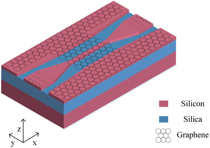
Figure 1.Schematic of GSHWs consisting of a graphene pad, a strip waveguide, and photonic crystal gratings.
Figure 3.(a)–(c) Real and imaginary parts of ERI and LAC at 500-nm width, 220-nm height, and 1550-nm wavelength with Fermi levels ranging from 0.12 eV to 0.6 eV for TE and TM modes, respectively. (d) The MDs are calculated with 10-μm-long graphene (the insets are electric field profiles of the TE mode at 1.4 and 1.7 μm wavelengths, respectively). (e) The MDs for TM mode under the same conditions.
The LAC (i.e., the linear limit of the SA [44]) of the in-plane monolayer graphene is obtained through [45]μwhere is the vacuum wavenumber, and subscript “imag” denotes the imaginary part of the ERI. The LAC is shown in Fig. 3(c) for TE and TM modes, respectively. As the two-level saturable absorber model is widely used in two-dimensional quantum wells, the absorption as a function of the light intensity can be fitted by , where is the threshold intensity of the SA, defined as the optical intensity required in a steady state to reduce the absorption to half of the unbleached value, and is the non-saturable absorption coefficient mainly determined by the scattering loss of graphene [3]. When the light intensity is high enough, the absorption coefficient of graphene is close to . Finally, the MD is given by [44,46,47]where is the length of graphene, and is the absorption coefficient of graphene mainly resulting from the interband transition of carriers and the scattering of graphene coming from the residual aggregates, contamination, wrinkles, and cracks [3,12,15].
Moreover, we simulate the dependence of the MD on wavelengths of incident light, Fermi levels, dimensions of GSHWs, and lengths of graphene pads. Figures 3(d) and 3(e) depict the dependence of the MD on wavelengths of incident light and Fermi levels of graphene for TE and TM modes, respectively. The GSHW with a width of 500 nm, a height of 220 nm, and a 10-μm-long graphene pad is pumped by a 1550-nm input light. As shown in Fig. 3(d), the larger values of the MD are achieved with longer incident wavelengths because stronger light–matter interaction is obtained by the longer incident wavelength, in comparison to that obtained by the shorter incident wavelength shown in the inset. Also lower doping level of graphene is also preferred owing to the larger absorption of graphene. As the TM mode is shown in Fig. 3(e), the increment of the MD over 2.5 times is obtained with shorter wavelengths because of the strengthened leaky field on top of the silicon waveguides, compared to the TE mode. The dependence of the MDs on Fermi levels implies that the values of the MDs can be changed through electronic doping and optical exciters.
Figure 4.(a), (b) Simulated MDs depending on the width and height of GSHWs with the Fermi level of 0.4 eV and 10-μm-long graphene pad for the TE and TM modes, respectively. (c) The dependence of MDs on the different lengths of graphene for the TE and TM modes with the 500-nm-wide waveguide and Fermi level of 0.4 eV.
Figure 5.(a) Raman spectra of the GSHWs (the inset figure is the SEM picture of graphene pad, the blue circle represents the spot where graphene is etched off, the red circle represents the spot where graphene is protected). (b) The experimental transmission data and fitted curves as a function of input power for the TE mode. Here, the relative transmission is expressed as . (c) The comparison of MDs in simulated and experimental results with 10-, 15-, 20-, and 30-μm-long graphene pads (the GSHW with 30-μm-long graphene is not saturated sufficiently with the maximum power of the femtosecond laser we use. Here, we use the fitted MD of 30.1% from the measured data).
Figure 5(a) exhibits the Raman spectra of the graphene pad which are acquired by a LabRAM HR800 with 532-nm excitation. The red curve shows a G peak () with a full width at half-maximum (FWHM) of , a 2D peak () with a 2D-to-G peak intensity ratio of about 1.6, and an inconspicuous D peak, implying the good quality of the transferred monolayer graphene with a Fermi level of about [49]. The blue curve shows no characteristic peaks of graphene, indicating the graphene is etched off effectively by RIE.
The LACs of the GSHWs are characterized by a cutoff method and the measured result is about 0.049 dB/μm, which is close to the simulated result (0.039 dB/μm). The error may come from the scattering loss of the graphene resulting from the process of CVD growth and transfer of graphene. A home-made femtosecond fiber laser with a center wavelength of 1560 nm (pulse width: , repetition rate: 92.9 MHz) is coupled into the GSHWs as a pump source. Four GSHWs with increasing lengths of graphene pads are applied for the SA measurement. The input light strongly interacts with graphene through evanescent coupling owing to the tight bonding between strip waveguides and graphene pads. As the intensity of light increases, the photogenerated carriers lead to the fulfillment of the states near the edge of the conduction and valence bands of graphene [3]. The SA or bleaching of incident light is achieved, resulting in a higher transmission of GSHWs.
As shown in the red triangles in Fig. 5(b), for the GSHW with a 10-μm-long graphene pad, the transmission increases non-linearly with rising input power. The averaged threshold power of the SA is 0.043 mW, corresponding to a threshold of 0.47 W in peak power (i.e., pulse energy of 423 fJ). For the compact silicon waveguide with an effective mode area of , the peak power density arrives at . In addition, the MDs of 500-nm-wide waveguides with 15-, 20-, and 30-μm graphene pads are also provided in blue triangles, green circles, and black squares in Fig. 5(b), exhibiting MDs of 13.6%, 16.4%, and 22.7% with the threshold powers of 0.054, 0.065, and 0.14 mW (i.e., pulse energies of 532, 641, and 1380 fJ), respectively. It is noted that the 30-μm-long graphene pad is not saturated sufficiently with the maximum power of the femtosecond laser we have (the MD can reach 30.1% according to the fitted data). The simulated results (9.7%, 13.6%, 16.4%, and 31.9%) from Fig. 4(c) are in good agreement with the experimental results from Fig. 5(b), which is shown in Fig. 5(c).
Here, the modulation efficiency, defined as the MD per unit length of the device, is about 0.033 dB/μm, which could be further approved by the enhancement of interaction between light and graphene [16,18]. Slot waveguides with smaller effective mode areas may improve modulation efficiency and reduce energy per pulse further [25]. Although the graphene pad with longer length increases the MD, more energy consumption is brought. In order to achieve enough MD and reasonable energy consumption, we choose GSHWs with 30-μm-long graphene in the following experiments of demonstration of all-optical modulation and the response time of the devices.
C. Demonstration of All-Optical Modulation of GSHWs and Response Time of Devices
Figure 6.(a) Schematic of the experimental system. (b) Time history of the modulated probe light with the pump light acquired by the oscilloscope (OSC). (c) Time profile of a probe pulse (the inset is the temporal profile of a pump pulse).
In summary, an all-optical modulator has been realized by the GSHW. The modulation depth reached 22.7% with a saturation threshold down to 1.38 pJ per pulse with a 30-μm-long graphene pad. The MD can be manipulated by the dimension of waveguides, length, and the Fermi level of graphene through electronic doping and optical exciters. An ultrashort response time of 1.65 ps was obtained by a pump–probe measurement with 2.1 pJ per pulse. The all-optical modulator based on GSHW, with the combined advantages of a compact footprint, broadband operation, the response time of few picoseconds, energy consumption of picojoule per pulse, and compatibility with CMOS, could bring us a step closer to realizing on-chip all-optical control.
Acknowledgment
Acknowledgment. We thank all engineers in the Center of Micro-Fabrication and Characterization (CMFC) of Wuhan National Laboratory for Optoelectronics (WNLO) for the support in fabrication.
[33] M. Ono, M. Hata, M. Tsunekawa, K. Nozaki, H. Sumikura, M. Notomi. Ultrafast and energy-efficient all-optical modulator based on deep-subwavelength graphene-loaded plasmonic waveguides. Conference on Lasers & Electro-Optics (CLEO), FF2L.4(2018).