Contents


2023
Volume: 11 Issue 4
21 Article(s)
Export citation format
Research Articles
Fiber Optics and Optical Communications
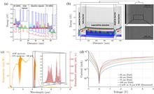
Interband cascade technology for energy-efficient mid-infrared free-space communication
Pierre Didier, Hedwig Knötig, Olivier Spitz, Laurent Cerutti... and Frédéric Grillot|Show fewer author(s)
Space-to-ground high-speed transmission is of utmost importance for the development of a worldwide broadband network. Mid-infrared wavelengths offer numerous advantages for building such a system, spanning from low atmospheric attenuation to eye-safe operation and resistance to inclement weather conditions. We demonstrate a full interband cascade system for high-speed transmission around a wavelength of 4.18 µm. The low-power consumption of both the laser and the detector in combination with a large modulation bandwidth and sufficient output power makes this technology ideal for a free-space optical communication application. Our proof-of-concept experiment employs a radio-frequency optimized Fabry–Perot interband cascade laser and an interband cascade infrared photodetector based on a type-II InAs/GaSb superlattice. The bandwidth of the system is evaluated to be around 1.5 GHz. It allows us to achieve data rates of 12 Gbit/s with an on–off keying scheme and 14 Gbit/s with a 4-level pulse amplitude modulation scheme. The quality of the transmission is enhanced by conventional pre- and post-processing in order to be compatible with standard error-code correction.Space-to-ground high-speed transmission is of utmost importance for the development of a worldwide broadband network. Mid-infrared wavelengths offer numerous advantages for building such a system, spanning from low atmospheric attenuation to eye-safe operation and resistance to inclement weather conditions. We demonstrate a full interband cascade system for high-speed transmission around a wavelength of
Photonics Research
- Publication Date: Mar. 27, 2023
- Vol. 11, Issue 4, 582 (2023)


Image Processing and Image Analysis
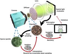
Learning-based super-resolution interpolation for sub-Nyquist sampled laser speckles
Huanhao Li, Zhipeng Yu, Qi Zhao, Yunqi Luo... and Puxiang Lai|Show fewer author(s)
Information retrieval from visually random optical speckle patterns is desired in many scenarios yet considered challenging. It requires accurate understanding or mapping of the multiple scattering process, or reliable capability to reverse or compensate for the scattering-induced phase distortions. In whatever situation, effective resolving and digitization of speckle patterns are necessary. Nevertheless, on some occasions, to increase the acquisition speed and/or signal-to-noise ratio (SNR), speckles captured by cameras are inevitably sampled in the sub-Nyquist domain via pixel binning (one camera pixel contains multiple speckle grains) due to finite size or limited bandwidth of photosensors. Such a down-sampling process is irreversible; it undermines the fine structures of speckle grains and hence the encoded information, preventing successful information extraction. To retrace the lost information, super-resolution interpolation for such sub-Nyquist sampled speckles is needed. In this work, a deep neural network, namely SpkSRNet, is proposed to effectively up sample speckles that are sampled below 1/10 of the Nyquist criterion to well-resolved ones that not only resemble the comprehensive morphology of original speckles (decompose multiple speckle grains from one camera pixel) but also recover the lost complex information (human face in this study) with high fidelity under normal- and low-light conditions, which is impossible with classic interpolation methods. These successful speckle super-resolution interpolation demonstrations are essentially enabled by the strong implicit correlation among speckle grains, which is non-quantifiable but could be discovered by the well-trained network. With further engineering, the proposed learning platform may benefit many scenarios that are physically inaccessible, enabling fast acquisition of speckles with sufficient SNR and opening up new avenues for seeing big and seeing clearly simultaneously in complex scenarios.Information retrieval from visually random optical speckle patterns is desired in many scenarios yet considered challenging. It requires accurate understanding or mapping of the multiple scattering process, or reliable capability to reverse or compensate for the scattering-induced phase distortions. In whatever situation, effective resolving and digitization of speckle patterns are necessary. Nevertheless, on some occasions, to increase the acquisition speed and/or signal-to-noise ratio (SNR), speckles captured by cameras are inevitably sampled in the sub-Nyquist domain via pixel binning (one camera pixel contains multiple speckle grains) due to finite size or limited bandwidth of photosensors. Such a down-sampling process is irreversible; it undermines the fine structures of speckle grains and hence the encoded information, preventing successful information extraction. To retrace the lost information, super-resolution interpolation for such sub-Nyquist sampled speckles is needed. In this work, a deep neural network, namely SpkSRNet, is proposed to effectively up sample speckles that are sampled below 1/10 of the Nyquist criterion to well-resolved ones that not only resemble the comprehensive morphology of original speckles (decompose multiple speckle grains from one camera pixel) but also recover the lost complex information (human face in this study) with high fidelity under normal- and low-light conditions, which is impossible with classic interpolation methods. These successful speckle super-resolution interpolation demonstrations are essentially enabled by the strong implicit correlation among speckle grains, which is non-quantifiable but could be discovered by the well-trained network. With further engineering, the proposed learning platform may benefit many scenarios that are physically inaccessible, enabling fast acquisition of speckles with sufficient SNR and opening up new avenues for seeing big and seeing clearly simultaneously in complex scenarios..
Photonics Research
- Publication Date: Mar. 30, 2023
- Vol. 11, Issue 4, 631 (2023)
Imaging Systems, Microscopy, and Displays
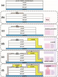
Systematic study on size and temporal dependence of micro-LED arrays for display applications
Junyang Nie, Zhi Zhang, Kongjie Chen, Yifeng Liu... and Qun Yan|Show fewer author(s)
Micro-LEDs are one of the most promising candidates for next-generation displays, yet they are inconvenienced by the efficiency reduction induced by the sidewall defects when pursuing further scaled-down device dimensions. We have systematically investigated both the size and temporal dependence of micro-LEDs. Micro-LED arrays with a mesa size ranging from 7 to 100 μm were prepared for display purposes. The luminance and external quantum efficiency (EQE) were measured and discussed. Surprisingly, micro-LED arrays with a smaller mesa size exhibit a higher EQE under 100 ns pulse duration operation when compared with longer pulse duration operations. Under certain short-pulsed excitation, a 7×7 μm2 micro-LED array even exhibits a >20% higher EQE as compared to the direct current (DC) or the long duration pulse operation condition. We thus concluded that the notorious efficiency reduction induced by sidewall defects in small-sized micro-LED arrays could be significantly reduced by applying short-pulse voltages.Micro-LEDs are one of the most promising candidates for next-generation displays, yet they are inconvenienced by the efficiency reduction induced by the sidewall defects when pursuing further scaled-down device dimensions. We have systematically investigated both the size and temporal dependence of micro-LEDs. Micro-LED arrays with a mesa size ranging from 7 to 100 μm were prepared for display purposes. The luminance and external quantum efficiency (EQE) were measured and discussed. Surprisingly, micro-LED arrays with a smaller mesa size exhibit a higher EQE under 100 ns pulse duration operation when compared with longer pulse duration operations. Under certain short-pulsed excitation, a
Photonics Research
- Publication Date: Mar. 09, 2023
- Vol. 11, Issue 4, 549 (2023)
Integrated Optics

Foundry manufacturing of tight-confinement, dispersion-engineered, ultralow-loss silicon nitride photonic integrated circuits | Spotlight on Optics
Zhichao Ye, Haiyan Jia, Zhangjun Huang, Chen Shen... and Junqiu Liu|Show fewer author(s)
The foundry development of integrated photonics has revolutionized today’s optical interconnect and datacenters. Over the last decade, we have witnessed the rising of silicon nitride (Si3N4) integrated photonics, which is currently transferring from laboratory research to foundry manufacturing. The development and transition are triggered by the ultimate need for low optical loss offered by Si3N4, which is beyond the reach of silicon and III-V semiconductors. Combined with modest Kerr nonlinearity, tight optical confinement, and dispersion engineering, Si3N4 has today become the leading platform for linear and Kerr nonlinear photonics, and it has enabled chip-scale lasers featuring ultralow noise on par with table-top fiber lasers. However, so far all the reported fabrication processes of tight-confinement, dispersion-engineered Si3N4 photonic integrated circuits (PICs) with optical loss down to few dB/m have only been developed on 4-inch (100 mm diameter) or smaller wafers. Yet, to transfer these processes to established CMOS foundries that typically operate 6-inch or even larger wafers, challenges remain. In this work, we demonstrate the first foundry-standard fabrication process of Si3N4 PICs with only 2.6 dB/m loss, thickness above 800 nm, and near 100% fabrication yield on 6-inch (150 mm diameter) wafers. Such thick and ultralow-loss Si3N4 PIC enables low-threshold generation of soliton frequency combs. Merging with advanced heterogeneous integration, active ultralow-loss Si3N4 integrated photonics could pave an avenue to addressing future demands in our increasingly information-driven society.The foundry development of integrated photonics has revolutionized today’s optical interconnect and datacenters. Over the last decade, we have witnessed the rising of silicon nitride (
Photonics Research
- Publication Date: Mar. 09, 2023
- Vol. 11, Issue 4, 558 (2023)

Regrowth-free AlGaInAs MQW polarization controller integrated with a sidewall grating DFB laser | Editors' Pick
Xiao Sun, Song Liang, Weiqing Cheng, Shengwei Ye... and Lianping Hou|Show fewer author(s)
Polarization control is at the heart of high-capacity data optical communication systems, such as polarization-division multiplexers and Stokes vector modulation transmitters. Despite passive polarization control being mature, the realization of monolithically integrated polarization controllers and single longitudinal mode light sources, such as distributed-feedback (DFB) lasers, is of importance. In this research, we report an AlGaInAs multiple-quantum-well photonic integrated circuit device which can control the state of polarization of the output light source, consisting of a polarization mode converter (PMC), a differential phase shifter (DPS), and a sidewall grating DFB laser. We demonstrate an asymmetrical stepped-height ridge waveguide PMC to realize TE to TM polarization conversion and a symmetrical straight waveguide DPS to enable polarization rotation from approximately counterclockwise circular polarization to linear polarization. Based on the identical epitaxial layer scheme, all the PMC, DPS, and DFB lasers can be integrated monolithically using only a single step of metalorganic vapor-phase epitaxy and two steps of III-V material dry etching. For the DFB-PMC device, a high TE to TM polarization conversion efficiency (98.4%) over a wide range of DFB injection currents is reported at 1555 nm wavelength. For the DFB-PMC-DPS device, a nearly 60° rotation of the Stokes vector on the Poincaré sphere was obtained with a range of bias voltage from 0 to -3.0 V at a laser drive current of 170 mA.Polarization control is at the heart of high-capacity data optical communication systems, such as polarization-division multiplexers and Stokes vector modulation transmitters. Despite passive polarization control being mature, the realization of monolithically integrated polarization controllers and single longitudinal mode light sources, such as distributed-feedback (DFB) lasers, is of importance. In this research, we report an AlGaInAs multiple-quantum-well photonic integrated circuit device which can control the state of polarization of the output light source, consisting of a polarization mode converter (PMC), a differential phase shifter (DPS), and a sidewall grating DFB laser. We demonstrate an asymmetrical stepped-height ridge waveguide PMC to realize TE to TM polarization conversion and a symmetrical straight waveguide DPS to enable polarization rotation from approximately counterclockwise circular polarization to linear polarization. Based on the identical epitaxial layer scheme, all the PMC, DPS, and DFB lasers can be integrated monolithically using only a single step of metalorganic vapor-phase epitaxy and two steps of III-V material dry etching. For the DFB-PMC device, a high TE to TM polarization conversion efficiency (98.4%) over a wide range of DFB injection currents is reported at 1555 nm wavelength. For the DFB-PMC-DPS device, a nearly 60° rotation of the Stokes vector on the Poincaré sphere was obtained with a range of bias voltage from 0 to
Photonics Research
- Publication Date: Mar. 30, 2023
- Vol. 11, Issue 4, 622 (2023)
Nanophotonics and Photonic Crystals

Perfect light absorber with a PT phase transition via coupled topological interface states
Jiajun Zheng, Haiyang Zhou, Junyang Li, Yufei Wang... and Hong Chen|Show fewer author(s)
Recently, the concepts of parity–time (PT) symmetry and band topology have inspired many novel ideas for light manipulation in their respective directions. Here we propose and demonstrate a perfect light absorber with a PT phase transition via coupled topological interface states (TISs), which combines the two concepts in a one-dimensional photonic crystal heterostructure. By fine tuning the coupling between TISs, the PT phase transition is revealed by the evolution of absorption spectra in both ideal and non-ideal PT symmetry cases. Especially, in the ideal case, a perfect light absorber at an exceptional point with unidirectional invisibility is numerically obtained. In the non-ideal case, a perfect light absorber in a broken phase is experimentally realized, which verifies the possibility of tailoring non-Hermiticity by engineering the coupling. Our work paves the way for novel effects and functional devices from the exceptional point of coupled TISs, such as a unidirectional light absorber and exceptional-point sensor.Recently, the concepts of parity–time (PT) symmetry and band topology have inspired many novel ideas for light manipulation in their respective directions. Here we propose and demonstrate a perfect light absorber with a PT phase transition via coupled topological interface states (TISs), which combines the two concepts in a one-dimensional photonic crystal heterostructure. By fine tuning the coupling between TISs, the PT phase transition is revealed by the evolution of absorption spectra in both ideal and non-ideal PT symmetry cases. Especially, in the ideal case, a perfect light absorber at an exceptional point with unidirectional invisibility is numerically obtained. In the non-ideal case, a perfect light absorber in a broken phase is experimentally realized, which verifies the possibility of tailoring non-Hermiticity by engineering the coupling. Our work paves the way for novel effects and functional devices from the exceptional point of coupled TISs, such as a unidirectional light absorber and exceptional-point sensor..
Photonics Research
- Publication Date: Mar. 09, 2023
- Vol. 11, Issue 4, 517 (2023)
Applications for wavelength division multiplexers based on topological photonic crystals
Yuhang Ruan, Xinyue Qian, Hai-Xiao Wang, Zheng-Da Hu... and Yixiang Wang|Show fewer author(s)
Topological edge states have an important role in optical modulation with potential applications in wavelength division multiplexers (WDMs). In this paper, 2D photonic crystals (PCs) with different rotation angles are combined to generate topological edge states. We reveal the relationship between the edge states and the rotation parameters of PCs, and further propose a WDM to realize the application of adjustable beams. Our findings successfully reveal the channel selectivity for optical transmission and provide a flexible way to promote the development of topological photonic devices.Topological edge states have an important role in optical modulation with potential applications in wavelength division multiplexers (WDMs). In this paper, 2D photonic crystals (PCs) with different rotation angles are combined to generate topological edge states. We reveal the relationship between the edge states and the rotation parameters of PCs, and further propose a WDM to realize the application of adjustable beams. Our findings successfully reveal the channel selectivity for optical transmission and provide a flexible way to promote the development of topological photonic devices..
Photonics Research
- Publication Date: Mar. 13, 2023
- Vol. 11, Issue 4, 569 (2023)
On-demand assembly of optically levitated nanoparticle arrays in vacuum
Jiangwei Yan, Xudong Yu, Zheng Vitto Han, Tongcang Li, and Jing Zhang
Realizing a large-scale fully controllable quantum system is a challenging task in current physical research and has broad applications. In this work, we create a reconfigurable optically levitated nanoparticle array in vacuum. Our optically levitated nanoparticle array allows full control of individual nanoparticles to form an arbitrary pattern and detect their motion. As a concrete example, we choose two nanoparticles without rotation signals from an array to synthesize a nanodumbbell in situ by merging them into one trap. The nanodumbbell synthesized in situ can rotate beyond 1 GHz. Our work provides a platform for studying macroscopic many-body physics and quantum sensing.Realizing a large-scale fully controllable quantum system is a challenging task in current physical research and has broad applications. In this work, we create a reconfigurable optically levitated nanoparticle array in vacuum. Our optically levitated nanoparticle array allows full control of individual nanoparticles to form an arbitrary pattern and detect their motion. As a concrete example, we choose two nanoparticles without rotation signals from an array to synthesize a nanodumbbell in situ by merging them into one trap. The nanodumbbell synthesized in situ can rotate beyond 1 GHz. Our work provides a platform for studying macroscopic many-body physics and quantum sensing..
Photonics Research
- Publication Date: Mar. 27, 2023
- Vol. 11, Issue 4, 600 (2023)
Non-Hermitian control of confined optical skyrmions in microcavities formed by photonic spin–orbit coupling
Xiaoxuan Luo, Yin Cai, Xin Yue, Wei Lin... and Feng Li|Show fewer author(s)
Optical skyrmions formed by photonic spin–orbit (SO) coupling are of significant interest in high-dimensional optical information processing. We report the formation mechanism and non-Hermitian properties of skyrmion-like states in a circular confinement potential with photonic SO coupling, which is preferably realized in a concave-planar microcavity system. We show that the effective photonic gauge field leads to two split manifolds of degenerate skyrmions whose spin textures can be controlled via the non-Hermitian properties by introducing circularly polarized gain and loss, exhibiting dramatically discrepant evolutions at the two sides of the exceptional point (EP). Furthermore, the lifetime degeneracy can be lifted by spatially inhomogeneous pumping according to the non-Hermitian mechanism, enabling the possibility for the skyrmion laser. By introducing shape asymmetry of the confinement potential, a double EP evolution can be achieved, which allows non-Hermitian control of the SO coupled states with higher degrees of freedom. These results open the way for the non-Hermitian control of photonic spin in confined systems, which would be of great significance for the fundamentals of advanced optical information processing.Optical skyrmions formed by photonic spin–orbit (SO) coupling are of significant interest in high-dimensional optical information processing. We report the formation mechanism and non-Hermitian properties of skyrmion-like states in a circular confinement potential with photonic SO coupling, which is preferably realized in a concave-planar microcavity system. We show that the effective photonic gauge field leads to two split manifolds of degenerate skyrmions whose spin textures can be controlled via the non-Hermitian properties by introducing circularly polarized gain and loss, exhibiting dramatically discrepant evolutions at the two sides of the exceptional point (EP). Furthermore, the lifetime degeneracy can be lifted by spatially inhomogeneous pumping according to the non-Hermitian mechanism, enabling the possibility for the skyrmion laser. By introducing shape asymmetry of the confinement potential, a double EP evolution can be achieved, which allows non-Hermitian control of the SO coupled states with higher degrees of freedom. These results open the way for the non-Hermitian control of photonic spin in confined systems, which would be of great significance for the fundamentals of advanced optical information processing..
Photonics Research
- Publication Date: Mar. 30, 2023
- Vol. 11, Issue 4, 610 (2023)
Optical and Photonic Materials
Tunable terahertz slow light with hybrid coupling of a magnetic toroidal and electric dipole metasurface
Guanchao Wang, Li Li, Chenxiang Liu, Shuai Li... and Hao Tian|Show fewer author(s)
We present a hybrid coupling scheme of a magnetic toroidal and electric dipole metasurface with suppressed radiation loss, which can produce the tunable plasmon-induced transparency (PIT) with an enhanced slow-light effect in the terahertz regime. The terahertz metasurface is constructed by nesting a dual-split ring resonator (DSRR) inside a ring resonator (RR) to exploit the destructive coherence of hybrid electromagnetic mode coupling at the PIT resonance. The polarization-dependence excitation performs the active tunability of a PIT-induced group slowing down by rotating the polarization angle, experimentally achieving a maximum group delay of 3.5 ps. Furthermore, the modified terahertz metasurface with a four-split ring resonator (FSRR) nested in an RR is prepared on photoconductive silicon, demonstrating the pump-controllable group delay effect at the PIT resonance. The large group delay from 2.2 to 0.9 ps is dynamically tunable by adjusting the pump power. The experimental results are in good accord with the theoretical simulations.We present a hybrid coupling scheme of a magnetic toroidal and electric dipole metasurface with suppressed radiation loss, which can produce the tunable plasmon-induced transparency (PIT) with an enhanced slow-light effect in the terahertz regime. The terahertz metasurface is constructed by nesting a dual-split ring resonator (DSRR) inside a ring resonator (RR) to exploit the destructive coherence of hybrid electromagnetic mode coupling at the PIT resonance. The polarization-dependence excitation performs the active tunability of a PIT-induced group slowing down by rotating the polarization angle, experimentally achieving a maximum group delay of 3.5 ps. Furthermore, the modified terahertz metasurface with a four-split ring resonator (FSRR) nested in an RR is prepared on photoconductive silicon, demonstrating the pump-controllable group delay effect at the PIT resonance. The large group delay from 2.2 to 0.9 ps is dynamically tunable by adjusting the pump power. The experimental results are in good accord with the theoretical simulations..
Photonics Research
- Publication Date: Mar. 09, 2023
- Vol. 11, Issue 4, 494 (2023)
Optoelectronics
Perovskite/GaAs-nanowire hybrid structure photodetectors with ultrafast multiband response enhancement by band engineering | Editors' Pick
Xiaobing Hou, Xitong Hong, Fengyuan Lin, Jinzhi Cui... and Zhipeng Wei|Show fewer author(s)
We developed a hybrid structure photodetector combining one-dimensional (1D) inorganic GaAs nanowires and two-dimensional (2D) organic perovskite materials, which can achieve various performance enhancements using a relatively simple structure. Via the optical absorption enhancement of perovskite and the type-II energy band structure formed by the heterostructure, the responsivity and detectivity of the photodetector from ultraviolet (UV) to visible (Vis) wavelengths are significantly enhanced, reaching 75 A/W and 1.49×10¹¹ Jones, respectively. The response time of the photodetector was significantly decreased by 3 orders, from 785 ms to 0.5 ms, and the dark current was further reduced to 237 fA. A photodetector was prepared with enhanced responsivity and ultrafast response time in the multiband region from the UV to Vis wavelength. To the best of our knowledge, this is the first time to combine inorganic III-V GaAs nanomaterials with organic perovskite materials, which verifies the effective combination of inorganic and organic materials in a mixed dimension. The excellent photoelectric performance of the perovskite/GaAs-nanowire hybrid structure photodetector makes it a potential candidate material for a wide range of photoelectric applications such as multiband photodetection.We developed a hybrid structure photodetector combining one-dimensional (1D) inorganic GaAs nanowires and two-dimensional (2D) organic perovskite materials, which can achieve various performance enhancements using a relatively simple structure. Via the optical absorption enhancement of perovskite and the type-II energy band structure formed by the heterostructure, the responsivity and detectivity of the photodetector from ultraviolet (UV) to visible (Vis) wavelengths are significantly enhanced, reaching 75 A/W and
Photonics Research
- Publication Date: Mar. 09, 2023
- Vol. 11, Issue 4, 541 (2023)
Quantum Optics
Continuous-variable quantum key distribution with on-chip light sources | On the Cover
Lang Li, Tao Wang, Xinhang Li, Peng Huang... and Guihua Zeng|Show fewer author(s)
Integrated quantum key distribution (QKD) systems based on photonic chips have high scalability and stability, and are promising for further construction of global quantum communications networks. On-chip quantum light sources are a critical component of a fully integrated QKD system; especially a continuous-variable QKD (CV-QKD) system based on coherent detection, which has extremely high requirements for the light sources. Here, for what we believe is the first time, we designed and fabricated two on-chip tunable lasers for CV-QKD, and demonstrated a high-performance system based on these sources. Because of the high output power, fine tunability, and narrow linewidth, the involved on-chip lasers guarantee the accurate shot-noise-limited detection of quantum signals, center wavelength alignment of nonhomologous lasers, and suppression of untrusted excess noise. The system’s secret key rate can reach 0.75 Mb/s at a 50 km fiber distance, and the secure transmission distance can exceed 100 km. Our results mark a breakthrough toward building a fully integrated CV-QKD, and pave the way for a reliable and efficient terrestrial quantum-secure metropolitan area network.Integrated quantum key distribution (QKD) systems based on photonic chips have high scalability and stability, and are promising for further construction of global quantum communications networks. On-chip quantum light sources are a critical component of a fully integrated QKD system; especially a continuous-variable QKD (CV-QKD) system based on coherent detection, which has extremely high requirements for the light sources. Here, for what we believe is the first time, we designed and fabricated two on-chip tunable lasers for CV-QKD, and demonstrated a high-performance system based on these sources. Because of the high output power, fine tunability, and narrow linewidth, the involved on-chip lasers guarantee the accurate shot-noise-limited detection of quantum signals, center wavelength alignment of nonhomologous lasers, and suppression of untrusted excess noise. The system’s secret key rate can reach 0.75 Mb/s at a 50 km fiber distance, and the secure transmission distance can exceed 100 km. Our results mark a breakthrough toward building a fully integrated CV-QKD, and pave the way for a reliable and efficient terrestrial quantum-secure metropolitan area network..
Photonics Research
- Publication Date: Mar. 09, 2023
- Vol. 11, Issue 4, 504 (2023)
Continuous variable quantum conference network with a Greenberger–Horne–Zeilinger entangled state
Yue Qin, Jingxu Ma, Di Zhao, Jialin Cheng... and Xiaojun Jia|Show fewer author(s)
Quantum conference (QC) is a cryptographic task in secure communications that involves more than two users wishing to establish identical secret keys among N users. The Greenberger–Horne–Zeilinger (GHZ) entangled state is the basic resource for quantum cryptographic communication due to the existence of multipartite quantum correlations. An unconditional and efficient quantum network can be established with a continuous variable (CV) GHZ entangled state because of its deterministic entanglement. Here, we report an implementation of QC scheme using a CV multipartite GHZ entangled state. The submodes of a quadripartite GHZ entangled state are distributed to four spatially separated users. The proposed QC scheme is proved to be secure even when the entanglement is distributed through lossy quantum channels and the collective Gaussian attacks are in the all lossy channels. The presented QC scheme has the capability to be directly extended to a larger scale quantum network by using entangled states with more submodes.Quantum conference (QC) is a cryptographic task in secure communications that involves more than two users wishing to establish identical secret keys among
Photonics Research
- Publication Date: Mar. 09, 2023
- Vol. 11, Issue 4, 533 (2023)
Silicon Photonics
Robust bound states in the continuum in a dual waveguide system
Zhiyuan Gu, Sen Jiang, Chang Liu, and Nan Zhang
Bound states in the continuum (BICs) provide a fascinating platform to route/manipulate waves with ultralow loss by patterning low-refractive-index materials on a high-refractive-index substrate. Principally, the phase of leaking channels can be manipulated via tuning the structural parameters to achieve destructive interference (i.e., the BIC condition), surprisingly leading to the total elimination of dissipation to the continuum of the substrate. Despite recent developments in BIC photonics, the BIC conditions can only be satisfied at specified geometric sizes for waveguides that dim their application prospects. Here, we propose a dual waveguide system that support BICs under arbitrary waveguide sizes by solely changing the intervals between the two waveguides. Our calculation results show that robust BICs in such architectures stem from the interaction (destructive interference) between leaking waves from the two waveguides. Furthermore, a cladding layer is introduced to improve the fabrication tolerance and reduce the sensitivity of the low-loss condition on the waveguide intervals of the presented dual waveguide system. The proposed approach offers an intriguing solution to establish a BIC concept and may be helpful to improve the potential of BIC photonic devices and circuits.Bound states in the continuum (BICs) provide a fascinating platform to route/manipulate waves with ultralow loss by patterning low-refractive-index materials on a high-refractive-index substrate. Principally, the phase of leaking channels can be manipulated via tuning the structural parameters to achieve destructive interference (i.e., the BIC condition), surprisingly leading to the total elimination of dissipation to the continuum of the substrate. Despite recent developments in BIC photonics, the BIC conditions can only be satisfied at specified geometric sizes for waveguides that dim their application prospects. Here, we propose a dual waveguide system that support BICs under arbitrary waveguide sizes by solely changing the intervals between the two waveguides. Our calculation results show that robust BICs in such architectures stem from the interaction (destructive interference) between leaking waves from the two waveguides. Furthermore, a cladding layer is introduced to improve the fabrication tolerance and reduce the sensitivity of the low-loss condition on the waveguide intervals of the presented dual waveguide system. The proposed approach offers an intriguing solution to establish a BIC concept and may be helpful to improve the potential of BIC photonic devices and circuits..
Photonics Research
- Publication Date: Mar. 13, 2023
- Vol. 11, Issue 4, 575 (2023)
Low temperature sensitivity on-chip Fourier-transform spectrometer based on dual-layer Si3N4 spiral waveguides
Liangjun Lu, Hongyi Zhang, Xin Li, Jianping Chen, and Linjie Zhou
On-chip Fourier-transform spectrometers (FTSs) based on Mach–Zehnder interferometer (MZI) arrays suffer from severe central wavelength and fringe contrast variation due to fabrication errors. Even though a calibration matrix can be employed to correctly retrieve the input spectra, environmental temperature variation greatly degrades the retrieving performance. In this paper, we devise a dual-layer Si3N4 waveguide interferometer to reduce the temperature sensitivity. The beating of the even and odd supermodes in the dual-layer waveguide generates periodic intensity fluctuations in the spectrum. Since these two modes have similar modal profiles, their thermal sensitivity and propagation loss are relatively balanced, leading to a low temperature sensitivity and a high interference extinction ratio. We designed and fabricated a passive FTS based on a 32-channel dual-layer Si3N4 waveguide array. Experimental results show that the temperature sensitivity is reduced to 10 pm/°C, which is almost half that of single-layer Si3N4 MZI-based FTSs. With this chip, we accurately reconstructed various types of optical spectra, including single and two sparse laser lines, and broadband optical spectra. Our method can fit a wide wavelength range, which is a promising technology to improve the practical applications of on-chip FTSs.On-chip Fourier-transform spectrometers (FTSs) based on Mach–Zehnder interferometer (MZI) arrays suffer from severe central wavelength and fringe contrast variation due to fabrication errors. Even though a calibration matrix can be employed to correctly retrieve the input spectra, environmental temperature variation greatly degrades the retrieving performance. In this paper, we devise a dual-layer
Photonics Research
- Publication Date: Mar. 27, 2023
- Vol. 11, Issue 4, 591 (2023)
Automatic synthesis of light-processing functions for programmable photonics: theory and realization | Editors' Pick
Zhengqi Gao, Xiangfeng Chen, Zhengxing Zhang, Uttara Chakraborty... and Duane S. Boning|Show fewer author(s)
Linear light-processing functions (e.g., routing, splitting, filtering) are key functions requiring configuration to implement on a programmable photonic integrated circuit (PPIC). In recirculating waveguide meshes (which include loop-backs), this is usually done manually. Some previous results describe explorations to perform this task automatically, but their efficiency or applicability is still limited. In this paper, we propose an efficient method that can automatically realize configurations for many light-processing functions on a square-mesh PPIC. At its heart is an automatic differentiation subroutine built upon analytical expressions of scattering matrices that enables gradient descent optimization for functional circuit synthesis. Similar to the state-of-the-art synthesis techniques, our method can realize configurations for a wide range of light-processing functions, and multiple functions on the same PPIC simultaneously. However, we do not need to separate the functions spatially into different subdomains of the mesh, and the resulting optimum can have multiple functions using the same part of the mesh. Furthermore, compared to nongradient- or numerical differentiation-based methods, our proposed approach achieves 3× time reduction in computational cost.Linear light-processing functions (e.g., routing, splitting, filtering) are key functions requiring configuration to implement on a programmable photonic integrated circuit (PPIC). In recirculating waveguide meshes (which include loop-backs), this is usually done manually. Some previous results describe explorations to perform this task automatically, but their efficiency or applicability is still limited. In this paper, we propose an efficient method that can automatically realize configurations for many light-processing functions on a square-mesh PPIC. At its heart is an automatic differentiation subroutine built upon analytical expressions of scattering matrices that enables gradient descent optimization for functional circuit synthesis. Similar to the state-of-the-art synthesis techniques, our method can realize configurations for a wide range of light-processing functions, and multiple functions on the same PPIC simultaneously. However, we do not need to separate the functions spatially into different subdomains of the mesh, and the resulting optimum can have multiple functions using the same part of the mesh. Furthermore, compared to nongradient- or numerical differentiation-based methods, our proposed approach achieves
Photonics Research
- Publication Date: Mar. 30, 2023
- Vol. 11, Issue 4, 643 (2023)
Bidirectional high sidelobe suppression silicon optical phased array
Huaqing Qiu, Yong Liu, Xiansong Meng, Xiaowei Guan... and Hao Hu|Show fewer author(s)
An optical phased array (OPA), the most promising non-mechanical beam steering technique, has great potential for solid-state light detection and ranging systems, holographic imaging, and free-space optical communications. A high quality beam with low sidelobes is crucial for long-distance free-space transmission and detection. However, most previously reported OPAs suffer from high sidelobe levels, and few efforts are devoted to reducing sidelobe levels in both azimuthal (φ) and polar (θ) directions. To solve this issue, we propose a Y-splitter-assisted cascaded coupling scheme to realize Gaussian power distribution in the azimuthal direction, which overcomes the bottleneck in the conventional cascaded coupling scheme and significantly increases the sidelobe suppression ratio (SLSR) in the φ direction from 20 to 66 dB in theory for a 120-channel OPA. Moreover, we designed an apodized grating emitter to realize Gaussian power distribution in the polar direction to increase the SLSR. Based on both designs, we experimentally demonstrated a 120-channel OPA with dual-Gaussian power distribution in both φ and θ directions. The SLSRs in φ and θ directions are measured to be 15.1 dB and 25 dB, respectively. Furthermore, we steer the beam to the maximum field of view of 25°×13.2° with a periodic 2λ pitch (3.1 μm). The maximum total power consumption is only 0.332 W with a thermo-optic efficiency of 2.7 mW/π.An optical phased array (OPA), the most promising non-mechanical beam steering technique, has great potential for solid-state light detection and ranging systems, holographic imaging, and free-space optical communications. A high quality beam with low sidelobes is crucial for long-distance free-space transmission and detection. However, most previously reported OPAs suffer from high sidelobe levels, and few efforts are devoted to reducing sidelobe levels in both azimuthal (
Photonics Research
- Publication Date: Mar. 31, 2023
- Vol. 11, Issue 4, 659 (2023)
Surface Optics and Plasmonics
Metamaterial-based octave-wide terahertz bandpass filters
Ali Maleki, Avinash Singh, Ahmed Jaber, Wei Cui... and Jean-Michel Ménard|Show fewer author(s)
We present octave-wide bandpass filters in the terahertz (THz) region based on bilayer-metamaterial (BLMM) structures. The passband region has a super-Gaussian shape with a maximum transmittance approaching 70% and a typical stopband rejection of 20 dB. The design is based on a metasurface consisting of a metallic square-hole array deposited on a transparent polymer, which is stacked on top of an identical metasurface with a subwavelength separation. The superimposed metasurface structures were designed using finite-difference time-domain (FDTD) simulations and fabricated using a photolithography process. Experimental characterization of these structures between 0.3 and 5.8 THz is performed with a time-domain THz spectroscopy system. Good agreement between experiment and simulation results is observed. We also demonstrated that two superimposed BLMM (2BLMM) devices increase the steepness of the roll-offs to more than 85 dB/octave and enable a superior stopband rejection approaching 40 dB while the maximum transmittance remains above 65%. This work paves the way toward new THz applications, including the detection of THz pulses centered at specific frequencies, and an enhanced time-resolved detection sensitivity toward molecular vibrations that are noise dominated by a strong, off-resonant, driving field.We present octave-wide bandpass filters in the terahertz (THz) region based on bilayer-metamaterial (BLMM) structures. The passband region has a super-Gaussian shape with a maximum transmittance approaching 70% and a typical stopband rejection of 20 dB. The design is based on a metasurface consisting of a metallic square-hole array deposited on a transparent polymer, which is stacked on top of an identical metasurface with a subwavelength separation. The superimposed metasurface structures were designed using finite-difference time-domain (FDTD) simulations and fabricated using a photolithography process. Experimental characterization of these structures between 0.3 and 5.8 THz is performed with a time-domain THz spectroscopy system. Good agreement between experiment and simulation results is observed. We also demonstrated that two superimposed BLMM (2BLMM) devices increase the steepness of the roll-offs to more than 85 dB/octave and enable a superior stopband rejection approaching 40 dB while the maximum transmittance remains above 65%. This work paves the way toward new THz applications, including the detection of THz pulses centered at specific frequencies, and an enhanced time-resolved detection sensitivity toward molecular vibrations that are noise dominated by a strong, off-resonant, driving field..
Photonics Research
- Publication Date: Mar. 09, 2023
- Vol. 11, Issue 4, 526 (2023)
Reconfigurable and nonvolatile terahertz lithography-free photonic devices based on phase change films
Xieyu Chen, Shoujun Zhang, Kuan Liu, Yuehong Xu... and Zhen Tian|Show fewer author(s)
High-performance terahertz (THz) devices with reconfigurable features are highly desirable in many promising THz applications. However, most of the existing reconfigurable THz elements are still limited to volatile responses, single functionality, and time-consuming multistep manufacturing procedures. In this paper, we report a lithography-free approach to create reconfigurable and nonvolatile THz components by exploring the reversible, nonvolatile, and continuous THz modulation capability of the phase change material Ge2Sb2Te5. As a proof of concept, THz gratings with significant Rayleigh anomalies and diffraction as well as ultrathin THz flat lenses with subwavelength and ultra-broadband focusing capabilities are designed and fabricated on ultrathin Ge2Sb2Te5 films using the presented photo-imprint strategy. Moreover, such a method can also be adopted to create more complex THz devices, such as Pancharatnam–Berry phase metasurfaces and grayscale holographic plates. With these findings, the proposed method will provide a promising solution to realize reconfigurable and nonvolatile THz elements.High-performance terahertz (THz) devices with reconfigurable features are highly desirable in many promising THz applications. However, most of the existing reconfigurable THz elements are still limited to volatile responses, single functionality, and time-consuming multistep manufacturing procedures. In this paper, we report a lithography-free approach to create reconfigurable and nonvolatile THz components by exploring the reversible, nonvolatile, and continuous THz modulation capability of the phase change material
Photonics Research
- Publication Date: Mar. 31, 2023
- Vol. 11, Issue 4, 669 (2023)
Errata

Enhancing THz fingerprint detection on the planar surface of an inverted dielectric metagrating: publisher’s note
Xueying Liu, Wei Chen, Yongjie Ma, Yinong Xie... and Jinfeng Zhu|Show fewer author(s)
This publisher’s note corrects the funding order in Photon. Res.10, 2836 (2022)10.1364/PRJ.472114.This publisher’s note corrects the funding order in Photon. Res.10 , 2836 (2022 )10.1364/PRJ.472114
Photonics Research
- Publication Date: Mar. 23, 2023
- Vol. 11, Issue 4, 581 (2023)
Interpulse stimulation Fourier-transform coherent anti-Stokes Raman spectroscopy: publisher’s note
Minjian Lu, Yujia Zhang, Xinyi Chen, Yan Li, and Haoyun Wei
This publisher’s note corrects the funding order in Photon. Res.11, 357 (2023)10.1364/PRJ.473841.This publisher’s note corrects the funding order in Photon. Res.11 , 357 (2023 )10.1364/PRJ.473841
Photonics Research
- Publication Date: Mar. 27, 2023
- Vol. 11, Issue 4, 609 (2023)

About the Cover
External cavity on-chip tunable light sources based on silicon nitride can support high performance long distance local oscillator continuous-variable quantum key distribution, paving the way for construction of integrated metropolitan quantum networks. See L. Li et al., pp. 504–516.

© Copyright 2018-2021 | Chinese Laser Press. All Rights Reserved 沪ICP备15018463号-20