1State Key Laboratory of High Power Semiconductor Lasers, College of Physics, Changchun University of Science and Technology, Changchun 130022, China
2State Key Laboratory for Chemo/Biosensing and Chemometrics, College of Semiconductors (College of Integrated Circuits), Hunan University, Changsha 410082, China
3Department of Laser Photoelectric Technology, Southwest Institute of Technical Physics, Chengdu 610041, China
4Department of Electrical and Electronic Engineering, Southern University of Science and Technology, Shenzhen 518055, China
5Zhongshan Institute of Changchun University of Science and Technology, Zhongshan 442000, China
We developed a hybrid structure photodetector combining one-dimensional (1D) inorganic GaAs nanowires and two-dimensional (2D) organic perovskite materials, which can achieve various performance enhancements using a relatively simple structure. Via the optical absorption enhancement of perovskite and the type-II energy band structure formed by the heterostructure, the responsivity and detectivity of the photodetector from ultraviolet (UV) to visible (Vis) wavelengths are significantly enhanced, reaching 75 A/W and Jones, respectively. The response time of the photodetector was significantly decreased by 3 orders, from 785 ms to 0.5 ms, and the dark current was further reduced to 237 fA. A photodetector was prepared with enhanced responsivity and ultrafast response time in the multiband region from the UV to Vis wavelength. To the best of our knowledge, this is the first time to combine inorganic III-V GaAs nanomaterials with organic perovskite materials, which verifies the effective combination of inorganic and organic materials in a mixed dimension. The excellent photoelectric performance of the perovskite/GaAs-nanowire hybrid structure photodetector makes it a potential candidate material for a wide range of photoelectric applications such as multiband photodetection.
1. INTRODUCTION
High performance photodetectors are widely used in optical imaging and sensing, environmental monitoring, chemical/biological sensing, and other fields [1,2]. Therefore, continuous improvement of the performance parameters of photodetectors has always been the focus of experimental research. As a typical III-V compound semiconductor material with a direct band gap (1.42 eV) and high electron mobility, GaAs nanowires (NWs) have recently attracted extensive attention in detection applications [3–5], making them suitable for preparing various photoelectric devices, such as solar cells [6,7], photodetectors [8,9], diodes [10], and field-effect transistors [11]. However, there are still many problems in the research on GaAs nanowire photodetectors. The inherently large specific surface area of one-dimensional nanowires leads to large surface defects, trapping photogenerated carriers and increasing the dark current, which affects the performance of photodetectors [8,12]. In addition, GaAs nanowires grown by conventional autocatalytic methods have many hanging bonds and form surface defects, which reduce the conductivity of the carriers and limit the performance of GaAs nanowire photodetectors. In the past decades, the dark current caused by sulfur passivation has been reduced [13,14], and doping carrier regulation photodetectors with multifunctional GaAs nanostructures such as built-in electric fields constructed by heterostructures, have achieved excellent photoconductivity [15–17]. However, few studies have been conducted on the performance of GaAs-based nanowire photodetectors. Most studies have only enhanced the single performance of GaAs nanowire photodetectors and few have comprehensively improved various properties. Owing to the limitations of the low optical absorption coefficient and the photoelectric conversion efficiency of GaAs nanowires, the responsivity and detectivity of GaAs nanowires are low, the response speed is slow, and the spectral response range is narrow, which limits the practical application of the GaAs photodetector. In addition, owing to its fixed electronic energy band structure, the absorption spectrum of single GaAs nanowires is limited to visible and near-infrared wavelengths. The study and application of GaAs nanowires based on UV wavelength are few, and the current demand for multiband detection by single-detection devices in imaging sensing and broadband optical communication is increasing [18,19], which is a serious challenge for single GaAs nanowires.
To realize the multiband photoelectric detection of GaAs nanowire photodetectors with enhanced performance in every aspect, we focus on recently emerging perovskite materials with improved performance [20–22]. Perovskite has been used in photovoltaic cells [23,24], light-emitting diodes [25,26], phototransistors [27–30], and photodetectors [31,32] because of its high absorption coefficient, tunable band gap, high quantum efficiency, and long carrier diffusion length [33,34]. However, the instability caused by the inherently low formation of three-dimensional perovskites seriously limits the use of perovskites in commercial applications. Therefore, recently, 2D Ruddlesden–Popper perovskite materials have been developed [35–37]. It inherits the three-dimensional (3D) perovskite, which has the general formula , where is an organic cation, is a metal ion, is a halide, and is the number of inorganic layers between organic chains. was used as an organic spacer. Because of the hydrophobicity of the organic spacer, this kind of 2D perovskite has good stability. Recently, studies on the structural evolution, electronic properties and optical response of this type of perovskite, such as the type, have been reported, in which represents and represents . When , the device performs better in many aspects because of its smaller optical band gap and denser microstructure [35]. In addition, when , the energy band of matches that of the GaAs.
Therefore, we combined a single GaAs nanowire photodetector with perovskite. This hybrid structure makes the perovskite and a single GaAs nanowire form a typical type-II energy band structure. Simultaneously, the high spectral absorption coefficient of the perovskite and type-II energy band structure significantly improved the response of the GaAs nanowire photodetector and the response time of the photodetector and allowed the perovskite to capture the defects on the surface of the nanowires and inhibit the recombination of carriers. The dark current was further reduced. Under the irradiation of a 375 nm laser, the perovskite/GaAs-nanowire photodetector achieved responsivity enhancement in the less studied UV wavelength region. A high-performance UV-Vis multiband photodetector based on a perovskite/GaAs-nanowire hybrid structure was successfully prepared.
Sign up for Photonics Research TOC. Get the latest issue of Photonics Research delivered right to you!Sign up now
2. EXPERIMENT
A. Preparation of GaAs Nanowire and Perovskite
GaAs NWs were grown using a self-catalyzed growth mechanism in a DCA P600 molecular beam epitaxy system. First, the silicon substrate was ultrasonically treated in ethanol for 5 min and then transferred to a preparation chamber for degassing at 400°C. Next, the Si substrate was shifted to the growth chamber to deposit Ga droplets at 620°C, and the growth was interrupted for 80 s. Subsequently, the nanowires (NWs) began to grow. During the growth process, the Ga beam equivalent pressure (BEP), the temperature, and the V-III ratio were set to (1 Torr = 133.32 Pa), 620°C, and 25, respectively. The growth process stopped after 1 h. The Ga source was switched off while supplying the As source until the substrate was cooled to 300°C. Finally, the temperature of the substrate was naturally reduced to room temperature. was prepared by dissolving stoichiometric quantities of MAI, PEAI, and in anhydrous -dimethylformamide. The resulting solution was continuously stirred at 50°C for 8 h inside a nitrogen-filled glovebox and filtered through a polytetrafluoroethylene syringe filter.
B. Fabrication of Perovskite/GaAs-Nanowire Photodetector
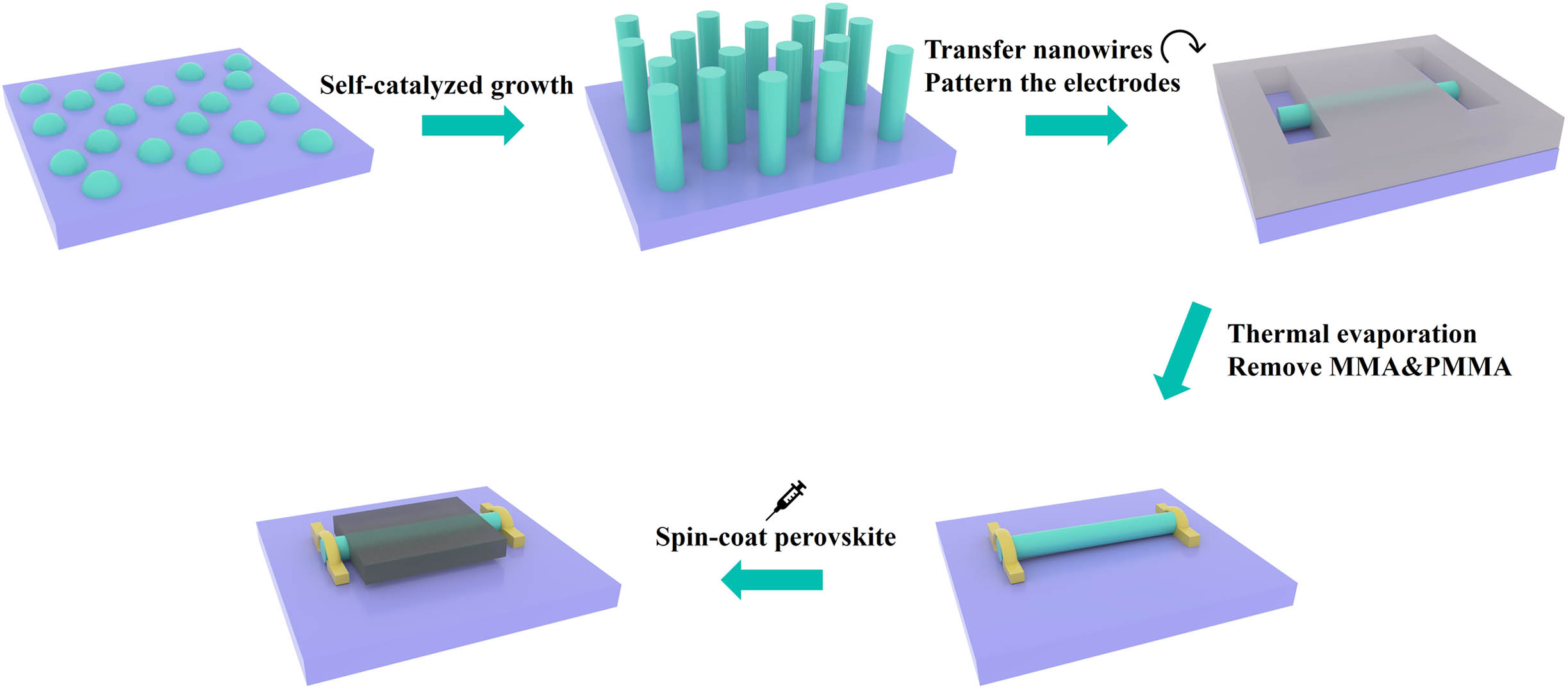
To fabricate the perovskite/GaAs NW photodetectors, GaAs NWs were first shifted to a marked silicon substrate with a 300-nm-oxide layer. The position of nanowires is determined by the Au mark. Then, the substrate was spin-coated with uniform methyl methacrylate (MMA) and poly(methyl methacrylate) (PMMA). After patterning the electrodes by electron beam lithography (JEOL JSM-IT300), Cr/Au (10/50 nm) was evaporated onto the substrate by thermal evaporation (JSD300). Acetone was used to remove the MMA, the PMMA, and the excess metal. The perovskite/GaAs-nanowire hybrid nanostructures were acquired through a crystallization process on individual GaAs nanowire devices. The perovskite precursor solution was spin-coated (3000 r/min) onto the as-fabricated single GaAs nanowire photodetector. The sample was then heated in air at 100°C (on a hot plate) for 1 h. The perovskite spin coating is applied to the entire Si substrate including the electrode. However, the perovskite does not directly contact the Cr at the bottom of the Au/Cr electrode, and the perovskite spin-coating on the electrode does not affect the performance of the photodetector. Subsequent experiments also proved that the photodetector performance originates from GaAs instead of perovskite. A schematic is shown without the perovskite covering the electrode to display the hybrid structure of the photodetector visually. The overall photodetector preparation process can be clearly understood from Fig. 1.
Figure 1.Schematic of the perovskite/GaAs-nanowire hybrid structure photodetector preparation process.
An Agilent 4155C semiconductor parameter analyzer was used to measure the electrical and optoelectronic properties of the single GaAs NW and the perovskite/GaAs NW hybrid structure photodetectors. The 375 nm and 532 nm lasers were applied with a series of luminous powers within the purview range of to measure the photoresponse of the photodetectors. All measurements for the photodetector were carried out in a vacuum at room temperature. A digital oscilloscope (GW Instek GDS-1102B) was used to test the response time of the photodetectors. The morphology of the samples was analyzed by a field emission scanning electron microscope (FESEM, TESCAN MIRA3 LMH) equipped with an energy dispersive X-ray spectroscopy (EDS) system (One Max 20). The UV-Vis spectra of a single GaAs nanowire, perovskite, and perovskite/GaAs-nanowire hybrid structure were measured using a spectrophotometer (U-3900H, Hitachi).
3. RESULTS AND DISCUSSION
Scanning electron microscopy (SEM) was performed to investigate the morphologies of the nanowire and perovskite materials. An SEM image of the GaAs nanowires grown by molecular beam epitaxy (MBE) is shown in Fig. 2(a). It can be observed that the length and diameter of the GaAs nanowires are approximately 6–8 μm and 150 nm, respectively. Figure 2(b) shows the two-dimensional surface, which is flat and smooth. An SEM image of the photodetector is shown in the Fig. 2(c). The channel length was set to 2 μm, which was later used to calculate the response of the photodetector, and the energy dispersive X-ray spectroscopy elemental mapping images of Ga, As, Pb, and I of the perovskite/GaAs-nanowire hybrid structure photodetector are shown in Fig. 2(d). The relative atomic content of Pb and I was 22.66% and 72.32% respectively, which is consistent with the elemental proportions of Pb and I in the perovskite we prepared.
Figure 2.(a) SEM image of as-grown GaAs NWs, (b) the perovskite surface, (c) the photodetector, and (d) the EDS elemental mapping images of the perovskite/GaAs hybrid structure photodetector.
To improve the performance of the GaAs nanowire photodetectors, we designed a perovskite/GaAs nanowire hybrid structure photodetector, which can improve the photodetector performance mainly through the energy band structure and light absorption enhancement. A schematic of the designed energy-band structure is shown in Fig. 3(a). The electron affinity and band gap width of the two materials constitute a typical type-II energy band structure [16,17,35]. The electrons in the conduction band of the GaAs nanowires enter the perovskite conduction band, and the holes in the valence band of the perovskite flow into the valence band of the GaAs nanowires to promote carrier separation. The hole carrier concentration in the GaAs nanowires was significantly increased. As a typical -type material [16,17], an increase in the hole carrier concentration will significantly increase the photocurrent of the GaAs nanowire photodetector. The absorption spectra measured in the micro-area of the single GaAs nanowire, perovskite, and perovskite/GaAs-nanowire hybrid structure are shown in Fig. 3(b). The GaAs nanowire measured in the micro-area was a single nanowire rather than nanowire arrays. The absorption coefficient is much lower compared with the perovskite and hybrid structure. The top perovskite layer of the hybrid structure acts as an absorption layer to provide excellent light absorption capability, which has a high optical absorption coefficient. The optical absorption of the hybrid structure is significantly enhanced compared with that of the single GaAs through the superimposed effect of spin-coating perovskite on a single nanowire [38]. The absorption peaks of the perovskite and hybrid structure are approximately 400 nm, indicating that the absorption enhancement of the spin-coated perovskite at the UV wavelength is stronger than that at the Vis wavelength. When light is incident on the hybrid structure, it is first incident on the perovskite material. The perovskite material will produce many photogenerated carriers through its large optical absorption coefficient, and then the light is further incident on the nanowire material and will also produce more photogenerated carriers owing to the enhanced optical absorption coefficient. While more photogenerated carriers are generated owing to the improvement of optical absorption, the perovskite and the GaAs nanowire are also affected by the type-II energy band structure to transport electrons and holes to each other, and the efficient charge separation by the type-II energy band structure further enhances the light absorption [39]. Ultimately, the photocurrent of the hybrid structure photodetector was significantly improved under the dual effects of producing more photogenerated carriers and hole inflow from the perovskite through the type-II energy band. The changes in the depletion region width and energy band structure before and after the formation of the hybrid structure by spin-coating perovskite are shown in Figs. 3(c) and 3(d), respectively. Owing to the difference in work functions between the metallic Cr and GaAs nanowire, the flow of electrons and holes generates a space electric field, which leads to the bending of the energy band and finally forms the depletion region. Owing to the enhanced light absorption and hole inflow from the perovskite, the hole carrier concentration of GaAs increased significantly. The Fermi energy level shifted to the valence band by increasing the hole concentration and squeezing the depletion region, reducing the width of the depletion region.
Figure 3.(a) Energy-band diagram of the perovskite/GaAs-nanowire hybrid structure. (b) The absorption spectra for the single GaAs nanowire, perovskite, and perovskite/GaAs-nanowire hybrid structure. The diagram with the change of energy band and depletion region width (c) before and (d) after spin coating perovskite.
The output characteristics of the perovskite are shown in Fig. 4(a). The photocurrent of the perovskite reached 260 pA at bias voltage at . A comparison of the dark current between the single nanowire and hybrid structure detector is shown in Fig. 4(b). The dark current decreased 8 times from 1.96 pA to 0.237 pA. The large dark current of the GaAs nanowires is due to the rich surface states. The surface states will capture electrons and cause the surface current to increase, resulting in a large final dark current. After spin-coating the perovskite, the decreased dark current was mainly due to the reduction in the surface state. The strongly bound inorganic ligand I in the perovskite replaces the trapped electrons and produces stable covalent bonds, which can passivate the surface of the GaAs nanowires [13,40]. The reduction of the surface traps reduces the probability of carriers being trapped on the surface of the GaAs nanowires, and the current can be transmitted more stably. Therefore, the dark current of the hybrid structure was significantly reduced. The photocurrents at 375 nm and 532 nm with different power intensities of the single GaAs nanowire photodetector are shown in Figs. 4(c) and 4(d), respectively. Under irradiation of the 375 nm and 532 nm lasers, the photocurrent of the single GaAs nanowire photodetector reached and at power density and bias voltage, respectively. The photocurrents at 375 nm and 532 nm with different power intensities of the perovskite/GaAs-nanowire hybrid structure photodetector are shown in Figs. 4(e) and 4(f). The photocurrent of the photodetector with the hybrid structure was significantly improved regardless of the 375 nm or 532 nm laser. Under the irradiation of the 375 nm and 532 nm lasers, the photocurrent of the perovskite/GaAs-nanowire hybrid structure photodetector reaches and at power intensity and bias voltage, respectively. The I-V curve of the hybrid structure has no obvious threshold voltage, and it has a larger photocurrent than that of the single GaAs nanowire, indicating that the hybrid structure photodetector has a better carrier separation ability to generate a hole that increases the photocurrent under light. This result is consistent with the design of the optical absorption enhancement from the perovskite materials and the formation of the type-II energy band structure. The light on/off ratio of the hybrid structure photodetector is as high as 20,760, which is much higher than that reported for GaAs nanowire photodetectors.
Figure 4.(a) The photocurrent of the single perovskite with different power intensities at 532 nm. (b) The dark current of the single GaAs nanowire and perovskite/GaAs-nanowire hybrid structure photodetectors. The photocurrent (c) at 375 nm and (d) at 532 nm with different power intensities of the single GaAs nanowire photodetector. The photocurrent (e) at 375 nm and (f) at 532 nm with different power intensities of the perovskite/GaAs-nanowire hybrid structure photodetector.
Figure 5(a) shows the photocurrent comparison of the perovskite, the GaAs, and the perovskite/GaAs hybrid structure photodetectors. It can be found that under the same optical power intensity, the photocurrent of the perovskite is the lowest, and it is also determined that the measured photodetector performance does not come from single perovskite. In addition, the photocurrent of the hybrid structure significantly improved at different optical power intensities. Figure 5(b) shows the photocurrent comparison of the single GaAs nanowire and hybrid structure photodetector with different optical power intensities at 375 nm and 532 nm wavelengths. The inset shows the absorption spectrum of single GaAs nanowire. The photocurrent of the photodetector at the 532 nm wavelength can be intuitively found to be stronger than that at the 375 nm wavelength, which is consistent with the absorption spectrum of the single GaAs nanowire. Comparing the absorption spectra between the single GaAs and the perovskite further proves that the performance determined is from the single GaAs nanowire instead of the perovskite. Responsivity (R) and specific detectivity (D*) are important parameters for measuring the performance of detectors. The responsivity is used to characterize the sensitivity of the photodetector and is defined as follows: where is the current obtained in the dark, is the current obtained under illumination, is the light illumination power density, and is the photosensitive region. Specific detectivity is an important parameter to measure the detector’s ability to detect weak signals, which can be defined as where is the electronic quantity. Figure 5(c) is the comparison of the responsivity at the 375 nm and 532 nm wavelengths of the hybrid structure. The responsivity showed a decreasing trend with the increase of the optical power intensity. The maximum responsivities at the wavelengths of 532 nm and 375 nm were 75 A/W and 13.5 A/W, respectively. Figures 5(d) and 5(e) show a comparison of the responsivity of the single nanowire and hybrid structure photodetector at wavelengths of 375 nm and 532 nm, respectively. The maximum responsivity of the hybrid structure photodetector is increased by approximately 13 times at 375 nm, while the maximum responsivity of the hybrid structure photodetector is only increased by 4.8 times at 532 nm, which is consistent with the different optical absorption enhancements of the absorption spectra at different wavelengths. Figure 5(f) shows the detectivity of the hybrid structure photodetector at 375 nm and 532 nm. Similarly, the detectivity at 532 nm is higher than that at 375 nm with different power intensities. The detectivity at 532 nm wavelength is up to Jones. The detectivity of the hybrid structure photodetector also decreases with the increase of the optical power intensity.
Figure 5.(a) The photocurrent comparison of perovskite, GaAs, and perovskite/GaAs hybrid structure photodetectors. (b) The photocurrent comparison at 375 nm and 532 nm wavelength of the single GaAs nanowire and perovskite/GaAs-nanowire hybrid structure photodetectors with the inset of the single GaAs nanowire absorption spectrum. (c) The responsivity of the hybrid structure photodetectors at 375 nm and 532 nm. The responsivity comparison of the single GaAs nanowire and hybrid structure photodetectors at (d) 375 nm and (e) at 532 nm. (f) Detectivity of the hybrid structure photodetectors at 375 nm and 532 nm wavelength.
Figure 6 shows the response time of the single GaAs nanowire and hybrid structure photodetectors at 532 nm wavelength. It can be clearly found that the rise and decay times of the hybrid structure photodetector decreased by 3 orders of magnitude. Rise time reduced from 568 ms to 1.2 ms, and decay time reduced from 785 ms to 0.5 ms. The response time of the photodetector is determined by many factors, including the carrier transit time in the depletion region, the carrier diffusion time outside the depletion region, and the lifetime of the electron trap state [41–43]. The carrier transit time is determined by the width of the depletion region. Therefore, the decrease in the width of the depletion region caused by the shift of the Fermi energy level to the valence band also reduces the carrier transit time. Therefore, while building heterostructures to inhibit carrier recombination and promote carrier separation and diffusion, the carrier transit time in the depletion region was also reduced, significantly improving the response speed. In addition, surface electrons may be the source of the slowly decaying continuous photocurrent, which mainly affects the decay time of the photodetector [44]. We can observe the same situation from Figs. 6(b) and 6(c), i.e., the decay time of the single GaAs nanowire is slower than the rise time because the nanowire surface exists in the surface state, which leads to a long discharge of the surface after the light is turned off, resulting in a slow decay time. The surface defects of the nanowires are covered by perovskite to reduce the number of surface electrons, resulting in the improvement of the photodetector response speed. Ultimately, the response time of the hybrid structure was significantly reduced through the above three aspects. As shown in Fig. 6(f), when the incident light is turned off, the current of the perovskite/GaAs-nanowire hybrid structure photodetector suddenly decreases to a very low dark current and then returns to the normal dark current. This phenomenon may be due to the carrier concentration imbalance and energy band regulation of the GaAs and the perovskite before and after the illumination. The GaAs and the perovskite lost incident light successively in an instant, and the photogenerated carriers corresponding to them decreased successively. When the perovskite material also loses incident light, the reduction of the photogenerated carrier concentration in the perovskite no longer maintains the hole flow into the GaAs, the hole concentration of them is out of balance, and the GaAs hole concentration is significantly higher than that of the perovskite, resulting in the hole backflow from GaAs into the perovskite material; the Fermi level also shifts up with the decreased hole concentration in the GaAs. Thus, the dark current suddenly decreased significantly more than the normal dark current, and the large reduction of dark current in the process of hole backflow led to the shorter decay time of hybrid structure photodetector. Then, the energy band structure returned to normal owing to the energy band regulation. The holes in the perovskite flowed into the GaAs, and the dark current returned to normal.
Figure 6.(a) The response time of three complete cycles of the single GaAs nanowire photodetector at 532 nm wavelength with (b) the rise and (c) decay times. (d) The response time of three complete cycles of the perovskite/GaAs hybrid structure photodetector at 532 nm wavelength with (e) the rise and (f) decay times.
In conclusion, we successfully prepared high-performance ultrafast multiband response hybrid structure photodetectors by combining a single inorganic GaAs nanowire and organic perovskite, which significantly improved the photocurrent in the multiband from UV to Vis wavelengths. Owing to the type-II energy band of the GaAs and the perovskite and the high optical absorption enhancement of perovskite, the responsivity and detectivity of the perovskite/GaAs-nanowire hybrid structure photodetector increased up to 75 A/W and Jones compared to the single GaAs nanowire photodetector, respectively. In addition, the response time reduced from 785 ms to 0.5 ms by 3 orders, the dark current was as low as 237 fA, and the light on/off ratio reached 20,760, which is higher than that of GaAs nanowire photodetectors reported now. This study provides an efficient method for combining multi-dimensional materials. The perovskite/GaAs nanowire hybrid photodetector has broad application prospects in the fields of optical communication, digital imaging, and night monitoring.