1Center for Terahertz Waves and College of Precision Instrument and Optoelectronics Engineering, Key Laboratory of Optoelectronic Information Technology (Ministry of Education of China), Tianjin University, Tianjin 300072, China
2School of Optoelectronic Engineering and Instrumentation Science, Dalian University of Technology, Dalian 116024, China
3Georgia Tech Shenzhen Institute (GTSI), Tianjin University, Shenzhen 518067, China
High-performance terahertz (THz) devices with reconfigurable features are highly desirable in many promising THz applications. However, most of the existing reconfigurable THz elements are still limited to volatile responses, single functionality, and time-consuming multistep manufacturing procedures. In this paper, we report a lithography-free approach to create reconfigurable and nonvolatile THz components by exploring the reversible, nonvolatile, and continuous THz modulation capability of the phase change material . As a proof of concept, THz gratings with significant Rayleigh anomalies and diffraction as well as ultrathin THz flat lenses with subwavelength and ultra-broadband focusing capabilities are designed and fabricated on ultrathin films using the presented photo-imprint strategy. Moreover, such a method can also be adopted to create more complex THz devices, such as Pancharatnam–Berry phase metasurfaces and grayscale holographic plates. With these findings, the proposed method will provide a promising solution to realize reconfigurable and nonvolatile THz elements.
1. INTRODUCTION
Terahertz (THz) technology focusing on the frequency regime ranging from 0.1 to 10 THz is the basis of next-generation, high-capacity wireless communications [1–3] and can also greatly promote the development of multiple applications, including nondestructive biosensing [4] and noninvasive imaging [5]. However, until now, most of these applications can only be achieved in laboratory conditions due to the shortage of high-performance, low-cost THz elements. Among them, reconfigurable devices are highly desirable due to their powerful capability to manipulate THz waves and the necessity for many applications, such as single pixel imaging, adaptive THz systems, and optical switching. The emergence of a dynamic metasurface whose response can be tuned by an external stimulus (i.e., thermal, electrical, or optical) has provided a promising solution to realize reconfigurable THz elements. In recent years, a number of reconfigurable metasurface designs based on microelectromechanical systems technology [6–8], active materials (semiconductors [9–12], graphene [13–16] and other 2D materials [17,18], liquid crystals [19–21], perovskites [22], and [23–26]), and transistors [27–29] have been proposed to dynamically manipulate the properties of THz waves, and considerable progress has been made in this field. Nevertheless, most of these approaches were limited to lithography-based complex fabrication procedures and single functionality determined by a passive metasurface part, which severely hinders the applicability of these THz devices.
Recently, a more flexible approach based on an all-optical imprint has been presented and used to create a series of reconfigurable THz elements [30–34]. Commonly, the THz manipulation capability of these devices was realized by spatially modulating the charge carrier distribution in a homogeneous semiconductor substate, such as silicon and GaAs, using an optical pump beam carrying a specific pattern. However, due to the volatile nature of photoinduced charge carriers in semiconductor materials, an external optical pump must be applied to maintain the modulation function of these devices, causing high energy consumption.
Alternatively, chalcogenide phase change materials (PCMs) have attracted increasing attention in the field of active photonics [35–37] due to their dramatic optical property contrast between the amorphous and crystalline phases and the nonvolatile phase transition feature. In the PCM family, germanium-antimony-telluride alloy (GST) was the most popular choice because of its relatively balanced performance between switching speed, retention time, and stability during multiple crystallization and re-amorphization cycles, which has been widely adopted in dynamical nanophotonic devices from IR to UV regimes [38–50]. Recently, the nonvolatile THz modulation ability of GST materials has been explored in some preliminary studies [51–59]. More importantly, it has also been demonstrated that the GST phase transition process can be induced by a single optical pulse [60,61]. These features make GST an extremely promising material platform for an all-optical imprint strategy. We note that a GeTe-based hybrid coding metasurface with an optical reconfiguration capability has been recently realized in the THz region [62]. In this work, optically coded THz devices were fabricated by a two-step aligned lithography process and can only work under the reflective mode, which is still limited to the complex fabrication procedure and inconvenient working mode.
Sign up for Photonics Research TOC. Get the latest issue of Photonics Research delivered right to you!Sign up now
Here, we presented and experimentally demonstrated a lithography-free photo-imprint strategy for the realization of reconfigurable and nonvolatile THz elements by exploring the reversible, nonvolatile and multilevel THz modulation capability of material during the phase transition process. First, the THz response of GST during the thermally stimulated crystallization and optically stimulated re-amorphization process was characterized to verify the remarkable THz modulation ability of this material. Then, to clearly show the effectiveness of the proposed photo-imprint strategy, the featured THz responses (i.e., Rayleigh anomaly and beam splitting of a series of optically written GST gratings), were experimentally measured. Next, ultrathin (100 nm) THz lenses with subwavelength focusing and ultra-broadband performance were designed, optically written, and experimentally characterized to further expand the application scope of the proposed GST photo-imprint strategy. Finally, the reconfigurable and multilevel modulation features of these flat lenses were also demonstrated. In addition to binary grating and flat lens devices, our technology can also be adopted to create more complex THz elements, including resonators, PB phase metasurfaces and nonvolatile spatial light modulators, which makes it a promising platform to realize reconfigurable and nonvolatile THz photonics.
2. RESULTS
A. THz Properties of GST Material
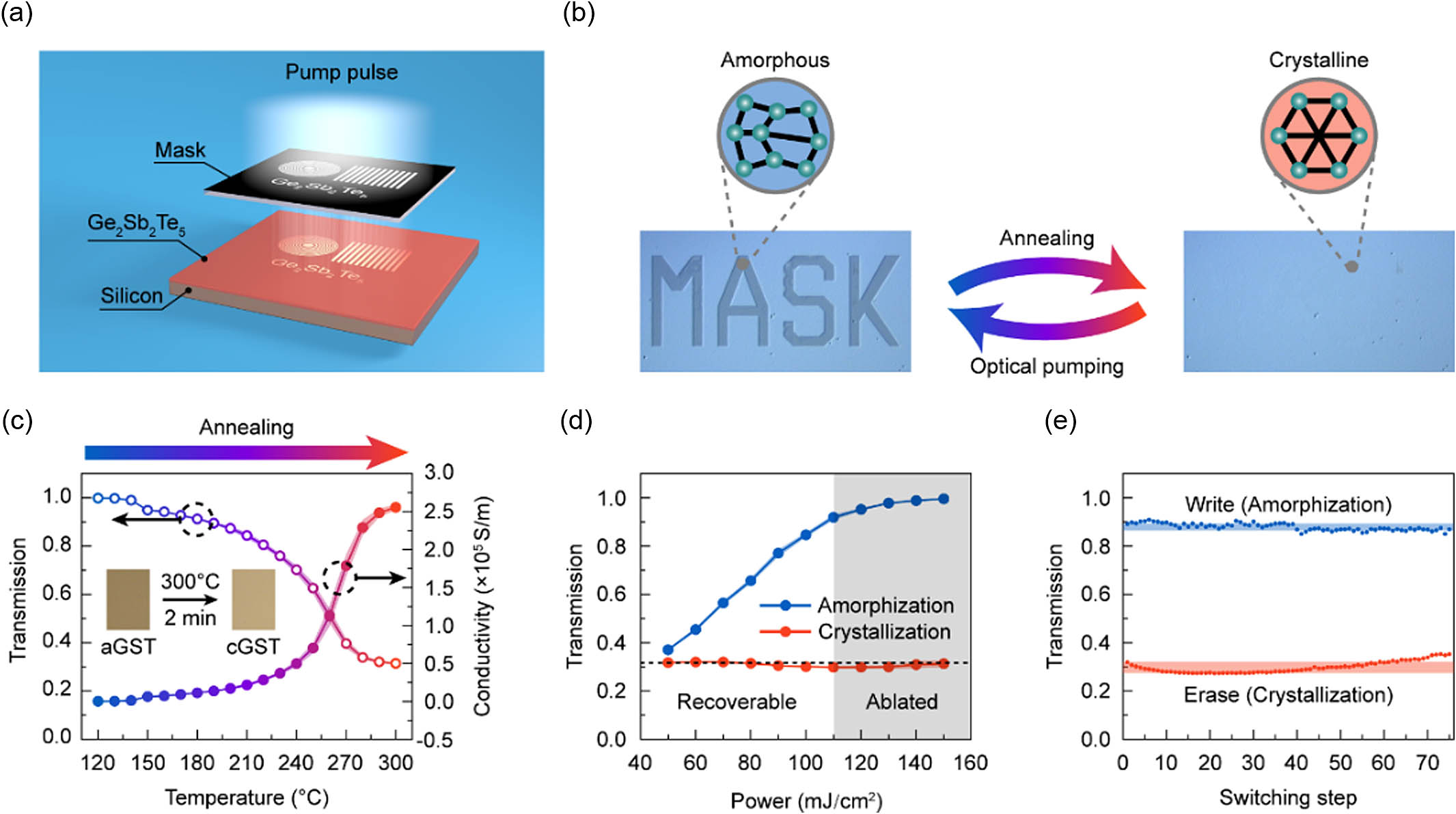
The applicability of (GST) for reconfigurable THz photonics mainly comes from its dramatic THz property contrast between three crystallographic phases [i.e., amorphous, metastable face centered cubic (FCC), and stable hexagonal close packed (HCP) states], which can be manipulated by properly applied thermal, electrical, or optical stimuli [53]. Interestingly, compared to the amorphous to HCP phase transition, which can hardly be induced by optical activation [60,63], the ultrafast HCP to amorphous phase change of GST can be realized via a nanosecond optical pump pulse-induced melt-quenching process [60,61]. Based on this property of GST, we present a photo-imprint strategy to create reconfigurable and nonvolatile THz devices. As schematically illustrated in Fig. 1(a), a single patterned pump pulse is used to spatially modulate the re-amorphization of crystalline GST, which results in a high-contrast pattern of the amorphous state on the GST film. By carefully designing the pump pattern, multiple binary elements such as gratings, Fresnel zone plates, and metasurfaces can be created. As a proof of concept, a “MASK” pattern was photo-imprinted onto a 100 nm thick GST layer with a pump power of , as shown in the left panel of Fig. 1(b). A significant dark area of the MASK can be observed due to the smaller reflection coefficient compared to the surrounding area, indicating the realization of spatially modulated re-amorphization of the GST film. Next, the sample was thermally annealed at 300°C for 2 min on a hot plate and is shown in the right panel of Fig. 1(b). After the thermal annealing process, the MASK pattern on the GST film vanishes along with the recrystallization of the amorphous area, and the homogeneous crystalline GST film can be further used in another photo-imprint fabrication. The demonstrated write (optically stimulated re-amorphization) and erase (thermally stimulated crystallization) processes of the GST film provide an attractive strategy to realize multiple THz diffractive elements.
Figure 1.Conceptual illustration of the photo-imprinted device and THz characterization of 100 nm thick GST. (a) Schematic view of photo-imprint concept. (b) Optical images of the GST layer after optical writing (left) and thermal erasing (right) processes. (c) Measured temperature-dependent transmission and corresponding conductivity of the GST film at 0.75 THz. Optical microscopy images of amorphous (left) and crystalline GST (right) are shown in the inset. (d) Measured 0.75 THz transmission of GST after the optical re-amorphization process under different pump energies (blue line) and followed the thermal recrystallization process (orange line). (e) Transmission at 0.75 THz of the same GST sample during multiple write (optical amorphization) and erase (thermal crystallization) cycles. Error bars with one standard deviation are shown by shaded areas along with data curves in (c)–(e).
As a preliminary work for element design, the THz properties of GST materials were first characterized. GST films (100 nm) were sputter deposited from a stoichiometric target onto a 1 mm thick high-resistivity silicon substrate and measured using a homemade THz time-domain spectroscopy (THz-TDS) system. We first exploit the THz response changes of GST during the thermally stimulated crystallization process. In the experiment, the amorphous to crystalline phase transition of GST was induced by annealing the sample from 120°C to 300°C with a step of 10°C and 2 min for each temperature gradient on a hot plate. The measured annealing temperature-dependent transmission at 0.75 THz of GST is shown in Fig. 1(c). Moreover, the corresponding THz conductivity real part of GST was also extracted using the film transmission formula [64] where is the wave impedance of vacuum, is the refractive index of the silicon substrate, and is the thickness of the deposited GST film. By increasing the annealing temperature from 120°C to 300°C, amorphous to FCC (approximately 150°C) and finally to HCP (approximately 260°C) phase transitions of GST can be induced, which can further be verified by the dramatic reflection contrast between the as-deposited and 300°C annealed GST samples, as shown in the inset of Fig. 1(c). During the process, the transmission significantly decreases from near 1 to 0.31 while there is a three-orders-of-magnitude increase in THz conductivity from to , indicating the outstanding THz tunability of the GST material.
To further explore the THz properties of GST during the re-amorphization process, a high-power 10 ns pulse laser working at a 1064 nm wavelength with a diameter of 1 cm was used to induce the re-amorphization of crystalline GST. The measured pump energy-dependent THz transmission at 0.75 THz of re-amorphized and corresponding re-crystallized GST (300°C annealed for 2 min) is illustrated in Fig. 1(d). According to the transmission of re-crystallized GST, the re-amorphization process of GST can be divided into two regions (i.e., recoverable and ablated regions), depending on the pump power. In the recoverable region, as the pump energy rises from 50 to , the transmission of GST rapidly increases from 0.37 to 0.92 due to the decrease in crystallinity and averaged THz conductivity of the GST film. Moreover, the small THz transmission of crystalline GST can be recovered by thermally annealing the re-amorphized GST sample at 300°C for 2 min, indicating that the GST layer can remain undamaged when the pump energy is lower than . For pump energies higher than , although the THz transmission can still be increased by raising the pump energy, the GST layer becomes damaged according to the transmission increase of the re-crystallized sample. Therefore, a pump power lower than should be adopted for the spatially modulated re-amorphization of GST in the next photo-imprint fabrication procedure. To further investigate the cyclability of our GST material, the transmission of 100 nm GST at 0.75 THz during 150 write (re-amorphization) and erase (recrystallization) cycles was measured and is shown in Fig. 1(e). In the experiment, the write and erase processes on GST were realized via optical and 300°C thermal activation, respectively. A relatively stable transmission switching between 0.88 (write) and 0.30 (erase) can be observed, indicating a good cyclability of GST during multiple optical write and thermal erase cycles. It should be noted that a slowly rising trend of THz transmission can be observed under the erase state due to the slight damage of GST induced by the optical pump, which can be solved by further decreasing the pump power. The demonstrated stable, reconfigurable, and nonvolatile modulation properties of GST are the basis of the presented photo-imprint strategy for on-demand THz diffractive element fabrication.
B. Photo-imprinted GST Grating Devices
Grating is one of the most common elements in optics and has been widely applied in multiple fields, including beam steering and spectroscopy. As a proof of the proposed fabrication strategy, we first photo-imprinted a THz grating structure onto a 100 nm GST film with optical pump energy. The period and duty cycle of the fabricated grating are 100 μm and 50%, respectively. As shown in Fig. 2(a), a high-quality grating structure composed of alternatively arranged amorphous and crystalline GSTs with excellent geometric parameters can be observed.
Sign up for Photonics Research TOC. Get the latest issue of Photonics Research delivered right to you!Sign up now
Figure 2.Photo-imprinted GST grating with reconfigurable Rayleigh anomaly. (a) Optical microscopy images of the GST grating (period is 100 μm and duty cycle is 50%) by using optical pump energy. (b) Measured transmission spectra of the GST grating (period and duty cycle fixed at 100 μm and 50%, respectively) with pump energy increasing from 50 to . The inset shows the transmission at a Rayleigh frequency of 0.87 THz as a function of pump energy. (c) Measured (stars) Rayleigh frequencies under different grating periods with a fixed pump energy of and calculated (blue line) period-dependent Rayleigh frequency.
To further explore the THz response of such a GST grating, a series of grating structures with fixed periods and duty cycles of 100 μm and 50%, respectively, were photo-imprinted under different pump powers ranging from 50 to . The measured transmission spectra of these gratings are summarized in Fig. 2(b). During the experiment, the electric field of the incident THz wave was polarized along the direction perpendicular to the grating lines. The transmission of the GST grating continuously increases with an increasing photo-imprint power, which can be attributed to the lower conductivity of re-amorphized GST regions under higher pump power. When the pump energy is higher than , a saturated transmission is reached due to the complete re-amorphization of GST. Moreover, we can also observe a pronounced spectral feature with strongly reduced transmission at approximately 0.87 THz under relatively high pump energy. We attribute such a transmission dip to the Rayleigh anomaly of grating, which occurs at the Rayleigh frequency if a diffracted order becomes tangent to the plane of grating. To confirm the physical mechanism of the transmission dip, we further photo-imprinted a set of GST grating structures with a fixed duty cycle of 50% and variable grating periods under a pump power of . The period-dependent transmission dip frequencies of fabricated GST gratings are extracted from measured spectra and illustrated in Fig. 2(c). Optical images of photo-imprinted gratings with periods of 40, 80, 150, 250, and 400 μm are also shown in Fig. 2(c), indicating the high quality of fabricated grating devices. In principle, the Rayleigh frequency is only determined by the period of grating and the refractive index of the substrate and given by under normal incidence [65], where is an integer and is the speed of light. To compare to the experimental results, the relationship between the Rayleigh frequency and grating period with and was calculated and is depicted by the blue line in Fig. 2(c). The excellent agreement between the experiment and theory proves that the transmission dips of photo-imprinted gratings indeed arise from the Rayleigh anomaly effect. Therefore, the high quality of the fabricated GST gratings has been demonstrated both by the optical images and the featured THz response of such devices, which further verifies the ability to create nonvolatile, reconfigurable, and multilevel THz elements of the presented photo-imprint strategy.
In addition to the Rayleigh anomaly, the beam steering ability based on diffraction is another important feature of the grating elements. However, the diffractive effect only occurs at wavelengths smaller than the period of grating. Thus, to further investigate the beam steering property of the photo-imprinted GST grating, a grating structure with a larger period of 800 μm and duty cycle of 50% was optically written onto a 100 nm GST film under a pump power of , as illustrated in the inset of Fig. 3(a). The diffractive transmission spectra of these GST gratings were measured using a homemade, all-fiber, angle-resolved THz-TDS system with an angle resolution of 1°. During the experiment, the normally-incident pulse THz wave was first modulated by the GST grating sample and collected by a photoconductive THz antenna with a detection angle ranging from to 85°. As shown in Fig. 3(a), apart from the zeroth-order, two significant diffraction beams with broadband features corresponding to the orders can also be observed. Moreover, based on the diffraction formula of grating, the dependence between frequency and diffraction angle was calculated by , where is the speed of light and μ is the period of grating. The calculated results are depicted by white dashed lines in Fig. 3(a). The excellent agreement between the calculation and experiment clearly verifies the high quality of the photo-imprinted GST grating.
Figure 3.Photo-imprinted GST grating with reconfigurable beam steering performance. (a) Measured diffractive transmission spectra of a GST grating photo-imprinted by a pump power of (period of 800 μm and duty cycle of 50%) for variable detection angles. The blue, green, and orange dashed lines illustrate the diffraction patterns at 20°, 30°, and 40°, respectively. The calculated frequency-dependent diffraction angle of order is depicted by the white line. The optical image of sample is shown in the inset. (b) THz signals and (c) corresponding spectra at 20°, 30°, and 40° diffraction angles. (d) Pump energy-dependent diffraction pattern of the GST grating (period and duty cycle fixed at 800 μm and 50%, respectively) at 20°, 30°, and 40°. (e) Measured and calculated relationship between THz signal frequency and diffraction angle of GST grating with different periods.
To further analyze the beam steering feature of the GST grating, the time-domain signals detected at 20°, 30°, and 40° were extracted and are shown in Fig. 3(b). Multicycle sinusoidal signals can be observed for all three detection angles, indicating the monochromatic nature of deflected THz beams under different angles. Moreover, the oscillation period of the THz signal significantly increases as the detection angle rises, indicating that the spectrum component with a lower frequency has a larger diffraction angle. This phenomenon can be observed more clearly from the Fourier transformation of the time-domain waveforms, as shown in Fig. 3(c).
Thus far, we have experimentally demonstrated the THz beam steering ability of photo-imprinted GST gratings. Next, we also study the effect of the grating period and pump power on the THz response of GST gratings. A series of GST gratings were photo-imprinted onto 100 nm GST films under different pump energies ranging from 60 to with a step of . The diffraction patterns at 20°, 30°, and 40° of these gratings were experimentally measured, as summarized in Fig. 3(d). A significant increasing trend of diffracted THz intensity can be observed for all detection angles as the pump energy rises, which can be attributed to the increased conductivity contrast between the crystalline and re-amorphous regions of the GST film. Next, GST gratings with different periods and a fixed duty cycle of 50% were photo-imprinted using pump power and experimentally characterized. The measured angle-dependent diffractive frequencies of these gratings are illustrated in Fig. 3(e), which show very good agreement with the theoretical curves calculated by the diffraction formula. According to the experimental results above, the diffractive effect and geometric parameters of the photo-imprinted GST grating can be conveniently modulated on demand by simply controlling the pump energy and carried pattern of the optical pulse, demonstrating the flexibility of the proposed photo-imprint strategy on a GST material.
C. Photo-imprinted GST Flat Lens
Recently, ultrathin flat lenses have attracted great attention due to the advantages of minimal aberration and high integration ability compared to conventional curved lenses. In the last decade, a few flat lens concepts have been proposed and demonstrated based on metasurfaces [66,67] and 2D materials [68–71]. However, the realization of ultrathin flat lenses with reconfigurable and nonvolatile properties in the THz region remains elusive. Here, we designed and experimentally demonstrated a reconfigurable and nonvolatile ultrathin (100 nm) flat THz lens with subwavelength and ultra-broadband focusing capabilities by using the proposed photo-imprint strategy on a GST film.
The design principle of the GST flat lens is schematically illustrated in Fig. 4(a). Such a flat lens can be seen as an amplitude-type Fresnel zone plate and the THz beams’ bending toward the focal point is caused by the diffraction effect [68,69]. Specifically, according to the propagation phase accumulation from the source points on the lens plane to the focal point, the lens plane can be divided into two regions: constructive interference region and destructive interference region. For the source points on the former region, constructive interference and thus the THz electrical field enhancement at the focal point can be achieved. However, the THz beams from the source points on the latter region will decrease the THz intensity of focal point due to destructive interference. Therefore, to maximize the THz intensity at the focal point, the interference condition must be optimized. One method is to modulate the initial phase of the source points on the destructive interference region, which is the design principle of a phase-type Fresnel zone plate. Another method is to reduce the amplitude of destructive interference THz beams, which can also enhance the THz intensity at the focal point. Considering that the transmission phase change induced by the GST layer is negligible resulting from the extremely small thickness of the GST film compared to the working wavelength of the flat lens(μ), the latter method was adopted and only the THz amplitude modulation of the GST layer was considered during the flat lens design.
Figure 4.Design and demonstration of a photo-imprinted GST flat lens. (a) Schematic view of the designed GST flat lens with a focus length of . (b) Conductivity and corresponding transmission distribution of the GST lens. (c) Optical image of a photo-imprinted flat lens on a 100 nm thick GST film with a pump power of . Theoretical focal intensity distributions of the GST lens (diameter of 1 cm and focal length of 5 mm) designed at 0.75 THz in the (d) axial and (e) lateral planes. Measured focal intensity distributions of fabricated GST flat lenses in the (f) axial and (g) lateral cross-sections at 0.75 THz. The lens working was photo-imprinted on a 100 nm thick GST film with pump energy. Extracted cross-sectional intensity distributions along the (h) z and (i) y directions.
According to the theory of the Fresnel zone plate discussed above, constructive interference of normally-incident THz waves can be achieved at the designed focal point by carefully dividing the GST plane into a set of alternately opaque and transparent radially symmetric regions. Next, we further quantitatively explain the design method for a GST flat lens. Assuming the focal length of the designed flat lens is , the propagation phase accumulation from the source point on the flat lens plane to the focal point can be calculated by where is the polar radius of the source point and is the wave vector of incident light. Then, the propagation phase difference between an arbitrary source point and the origin of the lens can be further expressed as where and represent the phase accumulation of the source point and the origin, respectively. According to interference theory, constructive interference at the focal point can be achieved for source points with . However, the light beams from the source points with will significantly decrease the light intensity of the focal point due to destructive interference. To maximize the focal intensity of the binary GST lens, the interference condition should be optimized by reducing the transmission of destructive interference THz beams. Therefore, the spatially modulated THz transmission of the GST layer was designed based on where and are the THz transmission of transparent and opaque regions of the GST flat lens, respectively. According to the experimental results in Section 2.A, we selected the THz transmission of re-amorphized and crystalline GST as and , respectively, to maximize the transmission modulation between transparent and opaque regions of the flat lens without causing GST damage. It should be noted that, because of the extremely small thickness of the GST film compared to the working wavelength of the flat lens (μ), the transmission phase change induced by the GST layer is very small. Therefore, only the THz amplitude modulation of the GST layer was considered during the flat lens design, while the phase modulation was ignored.
Based on the design concept above, we first designed a GST flat lens with 10 annular rings and a focal length of 5 mm at 0.75 THz. The GST conductivity and THz transmission distributions of the designed lens are illustrated in the left and right parts of Fig. 4(b), respectively. The GST flat lens is composed of alternately arranged annular regions with high and low THz transmission, which is realized by spatially manipulating the conductivity distribution of the GST layer.
To investigate the focal performance of the designed GST lens, the THz intensity distribution after modulation by the GST layer was numerically calculated based on the Rayleigh–Sommerfeld (RS) diffraction theory without considering the polarization of the incident field. In our calculation, a THz plane wave with uniform phase and amplitude was selected as the incident beam. The calculation was performed in the cylindrical coordinate system, and the axial coordinate of the flat lens was defined as . The electric field distribution behind the GST lens can be calculated by [72] where represents the electric field at point ; μ is the working wavelength of the flat lens; is the distance between the GST lens plane and the calculation plane; represents the electric field at point () on the GST plane; is the wave vector; and is the distance between the source point and the calculation point . The focal intensity distributions along the axial and lateral () directions are numerically calculated, as illustrated in Figs. 4(d) and 4(e), respectively. A well-defined strong focal point with negligible sidelobes can be observed in the focal plane. Moreover, according to Fig. 4(d), the calculated focal length of such a flat lens is approximately 5 mm, which agrees well with the design. These calculated results clearly demonstrate the effectiveness of the proposed GST flat lens design strategy.
To experimentally validate the design concept above, a GST lens working at 0.75 THz with a focal length of 5 mm was photo-imprinted on a silicon substrate-supported 100 nm crystalline GST layer under pump power, as illustrated in Fig. 4(c). Next, the focal performance of the fabricated GST flat lens was characterized using a homemade near-field scanning THz microscopy (NSTM) system [73]. During the experiment, the incident THz beam can be approximately seen as a quasi-plane wave with an electric field polarized along the y direction. The transmitted THz electric field of our GST flat lens was detected point-by-point using a mechanically scanned THz photoconductive probe with a 50 μm step in the x direction and y direction and a 100 μm step in the z direction. The measured focal intensity distributions along the axial and lateral () directions under 0.75 THz illumination are shown in Figs. 4(f) and 4(g), respectively. A significant focal effect with a well-defined focal point is achieved due to the two-level transmission modulation of the GST layer, which agrees well with the calculated results. The elliptical shape of the focal point observed in Fig. 4(g) can mainly be attributed to the asymmetric wave front of the incident beam. Then, we further extracted the THz intensity distributions along the propagation direction and the y direction to clearly see the difference between the calculation and experiment, as illustrated in Figs. 4(h) and 4(i), respectively. The measured focal length of the photo-imprinted GST flat lens is 300 μm smaller than the calculated result. This experimental error in focal length was caused because the incident THz beam was slightly focused instead being a perfectly collimated plane wave. However, the experimental intensity distribution curve along the y direction almost reproduces the theoretical plot with a measured FWHM value of approximately 315 μm, experimentally indicating the subwavelength focusing performance of the photo-imprinted GST flat lens. These experimental results clearly demonstrate the ability of the presented photo-imprint strategy to create a THz flat lens with ultrathin (100 nm) and subwavelength focusing properties on the GST material.
To further reveal the flexibility of the proposed GST photo-imprint strategy, a series of binary THz flat lenses with focal lengths ranging from 1 to 4 mm were designed and optically written on 100 nm GST films under pump energy. As depicted in the insets of Figs. 5(a), 5(c), 5(e), and 5(g), the alternately arranged dark and bright concentric ring regions for all the GST lenses can be clearly identified, verifying the high fabrication quality of these flat lenses. Then, the focal intensity distributions in the axial and lateral directions of the fabricated GST lenses were experimentally characterized using the NSTM system, as illustrated in Figs. 5(a)–5(h). Well-defined strong focus with ignorable sidelobes and subwavelength-scale focal points can be observed for all the GST lenses, indicating the high performance of these photo-imprinted flat lenses. Moreover, a significant decreasing trend of the FWHM from 272 μm to 171 μm along with a decrease in the designed focal length is observed, which can be attributed to an increase in the NA of the lenses. Then, the focal intensity distributions of GST lenses along the propagation and y directions were extracted and are illustrated in Figs. 5(i) and 5(j), respectively. The measured focal lengths of these four GST flat lenses are all smaller than the designed values, which is consistent with the results in Fig. 4 and can be explained by the slight focusing feature of the incident THz beam during the experiments. Interestingly, resulting from the broadband THz amplitude modulation property of the GST material, the focusing ability of the photo-imprinted GST flat lens can be maintained during an ultra-broadband region, as experimentally demonstrated in Fig. 7. According to the experimental results above, the ability of the presented GST photo-imprint strategy to create a broadband THz flat lens with subwavelength focusing performance and on-demand focal length has been fully demonstrated.
Figure 5.Photo-imprinted GST flat lens for variable focal lengths. Measured focal intensity distributions of the GST lens (pump energy fixed at ) with different focal lengths in the (a), (c), (e), and (g) axial and (b), (d), (f), and (h) lateral planes at 0.75 THz. The corresponding lens samples are shown in the insets with the same scale bar of 5 mm. Extracted cross-sectional intensity distributions for GST lenses with different focal lengths along the (i) z direction and (j) y direction.
As experimentally demonstrated in Fig. 1, the GST film can sustain a large number of optical write and thermal erase cycles without significant damage, which means that different THz functional devices can be repeatedly written and erased on the same GST film. To further explore the reconfigurable feature of the proposed photo-imprint strategy based on the GST material, the optical write and thermal erase cycles were carried out on the same 100 nm GST film twice. First, a flat lens with a 3 mm focal length was optically written on a crystalline GST film using a single pump pulse, as illustrated in the inset of Fig. 6(a). As shown in Figs. 6(a) and 6(e), the measured focal intensity distributions in the axial and lateral directions clearly show a strong focusing of the incident THz beam with subwavelength resolution and a focal length of approximately 2.8 mm. Then, the GST flat lens was thermally erased by annealing the sample at 300°C for 2 min. As depicted in the inset of Fig. 6(b), the amorphous GST regions were completely re-crystallized, and a uniform crystalline GST film was observed. Resulting from the high conductivity of crystalline GST, the transmitted THz intensity is very low, as illustrated in Figs. 6(b) and 6(f). Next, another flat lens with different focal lengths of 4 mm was rewritten on the same GST film, as shown in the inset of Fig. 6(c). The corresponding focal intensity distributions [Figs. 6(c) and 6(g)] clearly show a high-performance THz lens with a focal length of 3.7 mm, which agrees well with the design. Finally, after the thermal recrystallization procedure, the GST layer became uniformly crystalline and was ready for the next photo-imprint process with an on-demand pattern, as shown in Figs. 6(d) and 6(h). This reconfigurable property makes the proposed GST photo-imprint strategy a powerful method to realize reprogrammable THz functional elements.
Figure 6.Reconfigurable and multilevel modulation features of the photo-imprinted GST flat lens. Measured focal intensity distributions of the same GST sample during two write-erase cycles in the (a)–(d) axial and (e)–(h) lateral planes. The writing and erasing processes are realized by optical activation with pump energy and thermal activation at 300°C for 2 min, respectively. The corresponding optical images of the sample for each step are shown in the insets of (a)–(d). (i) Measured focal intensity of the photo-imprinted GST lens as a function of pump energy with error bars of one standard deviation. The focal intensity distributions in the lateral plane corresponding to different pump powers are also shown in the top panel.
Moreover, the fact that the THz amplitude modulation of GST is highly dependent on the optical pump power used in the GST re-amorphization process offers a simple yet effective method to tune the focal intensity of a photo-imprinted GST flat lenses. To experimentally validate the capability, we optically wrote a series of THz lenses with a fixed focal length of 3 mm and working frequency of 0.75 THz by using a single pulse with increasing pump energy from 50 to . The measured pump energy-dependent intensity distributions on the focal plane and corresponding focal intensities are illustrated in Fig. 6(i). The peak focusing intensity is found to increase monotonically with the pump energy, which can be attributed to the higher THz transmission contrast between the re-amorphized and crystalline GST regions of the flat lens. These results clearly show the multilevel modulation ability of our GST photo-imprint strategy, which provides a new degree of freedom to design and fabricate on-demand THz elements.
3. DISCUSSION
Note that the GST film thickness is an important parameter in THz device design. On the one hand, the surface conductivity of crystalline GST film (), which is linearly proportional to the GST thickness at a fixed conductivity of GST () according to , should be high enough to modulate the amplitude transmission of a THz wave. However, on the other hand, the limited penetration depth of the optical pump pulse used in the experiment and low thermal conductivity of the GST material made the complete re-amorphization of thicker crystalline GST film still a challenge. Thus, by balancing the experimental feasibility and the performance of GST devices, a 100 nm GST film was selected. As shown in the experimental results above, a GST film with a 100 nm thickness is thick enough for the design of multiple THz devices. Nevertheless, applying the photo-writable technique on thicker GST films is still an interesting research direction, which can further increase the application options. We believe that this goal could be achieved by these three different methods: (1) changing the center wavelength of laser source, (2) optimizing the intensity distribution of pump beam, and (3) optimizing the properties of GST via doping or controlling the growing environment.
As experimentally demonstrated, functional THz elements with reconfigurable and nonvolatile features, including gratings and flat lenses, can be realized by the GST photo-imprint strategy presented in this paper. The superior performance of these devices mainly results from the reversible, nonvolatile, multilevel, and stable modulation properties of the phase change material GST at the THz frequency. Compared to previous optical fabrication methods used to create reconfigurable functional elements in THz [33,34,62] and IR [38,39,74,75] regions, our technology has the following features. (1) The fabricated THz devices can be maintained for more than 10 years without any energy consumption due to the nonvolatile, stable properties of GST material, which is highly desirable, considering the issue of energy shortages. (2) In our design, THz modulation is achieved completely by the dramatic THz conductivity contrast between the amorphous and crystalline states of GST without any assisted microstructures, which makes the proposed photo-imprint strategy a simple, lithography-free method to realize reconfigurable THz devices. (3) Unlike previous pixel-by-pixel scanning-based optical fabrication technology, in our strategy, by exploring the optically stimulated re-amorphization of centimeter-level crystalline GST, the optically written process of functional THz devices can be achieved at ultrafast timescales (several nanoseconds) by using a single 10 ns laser pulse, which is much faster than previous works. Therefore, the proposed GST photo-imprint strategy is a promising technology to realize high-performance reconfigurable and nonvolatile flat THz elements.
In addition to the demonstrated grating and flat lens devices, the presented technology could also be used to create multiple binary THz elements, such as zone plates to generate focusing vortex beams with different topological charges [76], super-oscillatory lenses to realize THz super-resolution applications [77], resonators with on-demand THz response [38], PB phase metasurfaces [67] to manipulate circularly polarized THz waves, and nonvolatile spatial THz modulators. Note that to date, only binary THz devices have been demonstrated by the proposed GST photo-imprint method, while the multilevel modulation property of the GST material was not fully used due to the limitations of our experimental conditions. We believe that after the alignment problem is resolved by replacing the passive shadow mask with a spatial light modulator, the proposed strategy could also be used to fabricate more complex THz devices with multilevel amplitude modulation by simultaneously controlling the optical energy and pump pattern, such as blazed gratings [78] and grayscale holographic plates [38]. The great potential of the proposed GST photo-imprint strategy to fabricate a number of reconfigurable and nonvolatile THz devices is fascinating and will be further explored in future studies.
4. METHODS
A. Sample Preparation
First, the high-resistivity silicon substrates were cleaned by acetone, isopropanol, and deionized water in sequence. Then, 100 nm thick GST films were deposited by radio frequency (RF) sputtering a target onto pre-cleaned silicon substrates with an RF power of 30 W and chamber base pressure of ().
B. Optical Pump Parameters
In this work, a single 10 ns laser pulse with a 1064 nm center wavelength was used to re-amorphize the crystalline GST materials. During the experiment, the diameter of optical spot was fixed at around 10 mm (area of ), which was large enough to cover the THz spot. The pulse energy was tuned in the range of on demand to realize the multilevel amorphization of crystalline GST material, and thus the THz transmission.
5. CONCLUSION
In summary, we have presented and experimentally demonstrated a lithography-free photo-imprint strategy to realize reconfigurable and nonvolatile THz elements based on a phase change material of GST. First, the reversible, nonvolatile, and multilevel THz modulation ability of GST was experimentally verified by characterizing the THz response of the GST material during the thermally stimulated crystallization and optically stimulated re-amorphization processes. Next, as a proof of concept, a series of THz grating devices were photo-imprinted on 100 nm GST films. By experimentally characterizing the Rayleigh anomaly and diffractive responses of gratings, the high quality of fabricated gratings and thus the effectiveness of the proposed GST photo-imprint strategy were clearly demonstrated. Furthermore, using this technology, a set of reconfigurable and nonvolatile ultrathin (100 nm) THz flat lenses with subwavelength-scale and ultra-broadband focusing performance were also experimentally demonstrated. These results clearly show the effectiveness and flexibility of the proposed GST photo-imprint strategy, which makes it a promising solution to realize high-performance reconfigurable and nonvolatile THz devices.
APPENDIX A: BROADBAND FOCUSING FEATURE OF PHOTO-IMPRINTED GST FLAT LENS
To further investigate the broadband response of the proposed GST lens, a flat lens with focal length of 4 mm was optically written on a 100 nm GST layer by a single pump pulse. Then, the frequency dependent focal performance of such a GST lens was experimentally characterized using NSTM system and the measured results are shown in Fig. 7.
Figure 7.Flat lens with focal length of 4 mm was optically written on a 100 nm GST layer by a single pump pulse. The frequency dependent focal intensity distributions of such a GST lens along the (a) axial and (b) lateral directions were characterized using our NSTM system. (c) The THz intensity distributions along the x direction were also extracted to clearly see the FWHM of focal points for variable frequencies. Well-defined strong focusing effect with negligible sidelobes and subwavelength-scale FWHM of focal points can be observed for all the frequencies, which clearly demonstrates the broadband focusing feature of such photo-imprinted GST flat lenses.