An optical phased array (OPA), the most promising non-mechanical beam steering technique, has great potential for solid-state light detection and ranging systems, holographic imaging, and free-space optical communications. A high quality beam with low sidelobes is crucial for long-distance free-space transmission and detection. However, most previously reported OPAs suffer from high sidelobe levels, and few efforts are devoted to reducing sidelobe levels in both azimuthal () and polar () directions. To solve this issue, we propose a Y-splitter-assisted cascaded coupling scheme to realize Gaussian power distribution in the azimuthal direction, which overcomes the bottleneck in the conventional cascaded coupling scheme and significantly increases the sidelobe suppression ratio (SLSR) in the direction from 20 to 66 dB in theory for a 120-channel OPA. Moreover, we designed an apodized grating emitter to realize Gaussian power distribution in the polar direction to increase the SLSR. Based on both designs, we experimentally demonstrated a 120-channel OPA with dual-Gaussian power distribution in both and directions. The SLSRs in and directions are measured to be and , respectively. Furthermore, we steer the beam to the maximum field of view of with a periodic pitch (3.1 μm). The maximum total power consumption is only 0.332 W with a thermo-optic efficiency of .
1. INTRODUCTION
An optical phased array (OPA), as a novel solid-state beam steering technique, is becoming an alternative to the mechanical beam steering method that has been used in commercial light detection and ranging (LiDAR) systems [1–4]. OPAs are arrays of coherent optical emitters, with a working principle similar to the phased array antennas in radio waves. The far-field optical beam can be steered through the interference of emissions by controlling the phase of each emitter. Since OPA can be achieved on an integrated platform, it features a small size, weight, power, and cost (SWaP-C). It can be mass produced for various applications such as LiDAR [5–8] and free-space optical communication [9]. To date, integrated OPAs have been achieved on various integrated platforms such as silicon (Si) [10–17], Si nitride () [18], lithium niobate () [19], and indium phosphide (InP) [20]. Among them, Si is a desirable platform since it is fully compatible with the complementary metal oxide semiconductor (CMOS) fabrication process, allowing for integration with electronic controlling circuits [11,12].
Recently, research on integrated OPAs has mainly focused on scalability [11–13,21], field of view (FoV) [13,14,22], high resolution [14], and low power consumption [23], while few works achieve a high sidelobe suppression ratio (SLSR). SLSR is a crucial parameter for integrated OPAs, which determines the beam quality and is a bottleneck for many applications such as long-distance free-space optical communication.
Conventional OPAs with uniform emission have a pattern in the far field, resulting in a theoretical minimum sidelobe level of . By applying a Gaussian power distribution, sidelobes can be suppressed with the cost of a reduced effective emitting area. In 2019, Xie et al. demonstrated a 32-channel OPA and achieved a SLSR in azimuthal () direction using a star coupler for Gaussian amplitude distribution [24]. Moreover, there has been a recent demonstration that achieved 19 dB SLSR in azimuthal () direction for a 64-channel OPA by Liu and Hu using a star coupler as well [13]. However, to the best of our knowledge, applying Gaussian power distribution in both azimuthal () and polar () directions to achieve high sidelobe suppression has not been achieved yet.
Sign up for Photonics Research TOC. Get the latest issue of Photonics Research delivered right to you!Sign up now
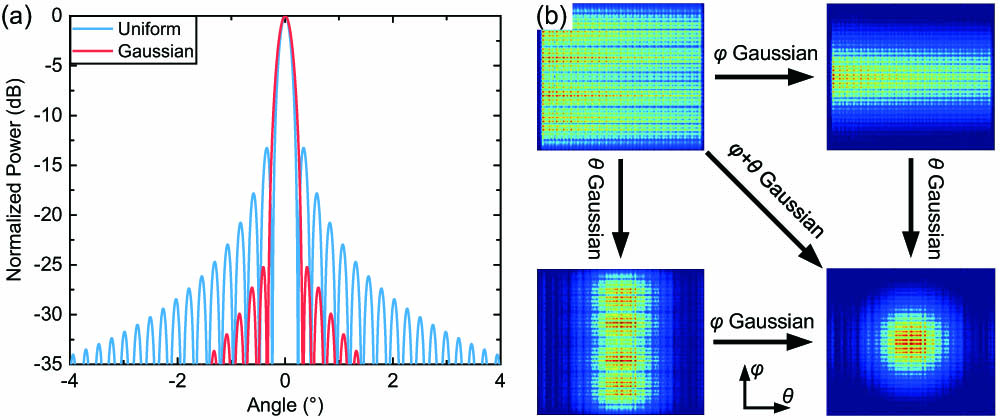
Figure 1.(a) Simulation results for uniform power distribution and Gaussian power distribution. (b) Simulated near field of uniform power distribution and Gaussian power distribution for direction, direction, and direction.
Here, we propose novel Y-branch-assisted cascaded directional couplers and a specially designed apodized grating emitter to achieve Gaussian power distribution in both and directions simultaneously. We fabricate and demonstrate a 120-channel one-dimensional (1D) OPA with a periodic 3.1 μm pitch. A steering range of () is achieved with the beam divergence of . The total power consumption of the OPA is 0.332 W. The measured SLSRs in and directions are 15.1 and 25 dB, respectively.
2. DEVICE DESIGN
The formulas below describe the near-field and far-field patterns of the periodic OPA: where is the emitter position in x-space, and and describe the near-field and far-field patterns in x-space and u-space, respectively. The near field of the periodic OPA can be regarded as the multiplication between the envelope and the Dirac comb with a periodic pitch of . After Fourier transformation, the far-field pattern can be described by Eq. (2). Assuming that the power is equally distributed on each channel, the rectangular envelope of in the near field will be Fourier transformed to the Sinc-function pattern in the far field. Therefore, the theoretical SLSR limitation is calculated to be 13.26 dB. An effective method to increase SLSR is by applying Gaussian power distribution in the near field. As a result, the far-field power distribution will be a Gaussian function as well, and the sidelobe can be suppressed. Figure 1(a) shows the simulated far-field power distribution for both uniform OPA (blue curve) and Gaussian OPA (red curve) with a periodic pitch of 3.1 μm. The SLSR is significantly increased to 25 dB when a 12 dB (center-to-edge ratio) Gaussian power distribution is applied to the near field instead of uniform power distribution. The simulated near-field power distributions are shown in Fig. 1(b). From the upper left to right bottom figure, the near field is changed from uniform to Gaussian power distribution in both directions, which can enable a high SLSR ( in theory).
A. Direction: Y-Splitter-Assisted Cascaded Coupling
Figure 2.(a) Schematic of the through-type cascaded coupler with Gaussian power distribution. (b) Required power, residual power, and coupling efficiency for the largest Gaussian center-to-edge ratio. (c) The largest SLSR is only 20 dB for the through-type cascaded coupler. (d) Schematic of the Y-branch-assisted cascaded coupler with Gaussian power distribution. (e) Required power, residual power, and coupling efficiency for the largest Gaussian center-to-edge ratio. (f) The largest SLSR can achieve 66 dB for the Y-branch-assisted cascaded coupler.
An improved scheme is Y-junction-assisted cascaded couplers, as shown in Fig. 2(d). Different from through-type cascaded couplers, light is coupled from the center to both sides; therefore, the required power and residual power for the first coupler (i.e., No. 60 channel or No. 61 channel in the center) are the largest simultaneously. Consequently, the coupling efficiency is not limited by the minimum coupling efficiency. The calculated coupling efficiencies for different channels are shown in Fig. 2(e). The corresponding largest SLSR can reach 66 dB in theory. Furthermore, we explore the scalability of the two types of cascaded couplers: Y-junction-assisted cascaded couplers can support 1024 channels even with 12 dB 140 Gaussian power distribution (see Appendix A.3), while through-type cascaded couplers can support only 420 channels and only for uniform power distribution (see Appendix A.2).
Figure 3.(a) Designed 12 dB Gaussian power distribution on 120-channel OPA. (b) Far-field figure with SLSR of 25 dB. (c) Required power, residual power, and coupling efficiency for each channel. (d) Coupling length for each channel.
Even though Y-junction-assisted cascaded couplers can increase the SLSR up to 66 dB in theory by using 51.7 dB Gaussian power distribution, it is difficult to observe such a large SLSR using an infrared camera, which typically has a dynamic range of only 30 dB. In the experiment, we design 12 dB Gaussian power distribution [Fig. 3(a)] of the 120-channel OPA, which can theoretically realize a 25 dB SLSR in direction [Fig. 3(b)]. The calculated coupling efficiency and coupling length for each channel are shown in Figs. 3(c) and 3(d), respectively.
B. Direction: Apodized Grating Emitter
So far, few schemes have paid attention to Gaussian power distribution in direction to increase the SLSR. One way to achieve this is an apodized grating emitter, which is usually used to decrease the coupling loss from the waveguide to the single-mode fiber (SMF) by reshaping the diffracted power distribution in the near field [25]. A schematic of the apodized grating emitter is shown in Fig. 4(a). We design the length, etching depth, and pitch of 2 mm, 10 nm, and 0.7 μm, respectively. The near-field power distribution can be reshaped by adjusting the duty cycle (etched part) for each emitting unit (), as shown in Fig. 4(b) (see Appendix A.4).
Figure 5.(a) Designed 12-dB Gaussian power distribution along 2-mm-long apodized grating emitter. (b) Corresponding SLSR in the far-field figure. (c) Simulated emitting efficiency per pitch and duty cycle along the apodized grating emitter. (d) The adjusted value of pitches guarantees the beam in the same direction.
Figure 6.(a) Schematic of proposed dual-Gaussian power distribution OPA. (b) Microscopy of proposed OPA. (c) SEM image of the apodized grating emitter with the largest duty cycle.
Considering the smallest feature size in the fabrication process, we design 12 dB Gaussian power distribution along the apodized grating emitter [Fig. 5(a)], which can achieve an SLSR of 25 dB [Fig. 5(b)]. The emitting efficiency of each unit and corresponding duty cycle are shown in Fig. 5(c). According to the grating formula, i.e., , the effective refractive index will vary when the duty cycle changes. To precisely converge the far-field beam, the pitch of each unit along the apodized grating emitter is adjusted, and the result is shown in Fig. 5(d) (see Appendix A.4).
3. DEVICE FABRICATION
A schematic of the 120-channel OPA with Gaussian power distribution in both directions is shown in Fig. 6(a). The OPA consists of the coupler, Y-branch-assisted cascaded couplers, energy-efficient thermo-optic phase shifters [26,27], and apodized grating emitters. The optical path of each channel from the Y-branch to the apodized grating emitter is specially designed to be the same length to ease the phase alignment. Every three phase shifters are combined as a group and share a common ground to match the I/O ports of a commercial field programmable gate array (FPGA). The adjacent phase shifters are periodically placed with a minimum pitch of 107 μm to eliminate thermal cross talk.
The 120-channel OPA is fabricated on a commercial Si-on-insulator (SOI) chip. First, we utilize E-beam lithography (EBL) and deep reactive ion etching (DRIE) to pattern the fully etched passive waveguide. Second, we repeat the processes to pattern and etch the 10 nm deep apodized grating emitter. Third, a 1 μm thick layer of Si dioxide () is deposited by plasma-enhanced chemical vapor deposition (PECVD) to clad the Si waveguide. The layer aims to protect the Si waveguide from being damaged, and decrease the optical loss caused by the metal layer that will be deposited on top. Fourth, we deposit the Ti layer as the micro-heater. Due to the large heater width (3 μm) designed in the phase shifter [27], ultraviolet (UV) lithography (375 nm wavelength) is used to define the heater pattern, followed by a layer of 110 nm thick Ti deposition using the E-beam evaporator (EBE) process. After the lift-off process, the Ti heater is fabricated. Last, we deposit a 500 nm thick layer of Au with the same process to act as the gold line to connect the chip with the printed circuit board (PCB). The microscope image is shown in Fig. 6(b). The average resistance is measured to be . Figure 6(c) indicates the scanning electron microscope (SEM) image of the apodized grating emitter. The largest etching width of the apodized grating emitter is 235 nm, which matches well with the designed value, i.e., μ (largest duty cycle) = 210 nm.
4. EXPERIMENT
A schematic of the far-field measurement setup is shown in Fig. 7(a). The chip-PCB is mounted on the fixed stage, which is placed in the center of a round rotation stage. The infrared camera is mounted on the round rotation stage, which can achieve a flexible rotation of 360°. A convex lens is mounted in front of the infrared camera to realize Fourier transformation between the near-field and far-field figures. Therefore, the far-field figure can be obtained at a short distance, i.e., in the image focal plane of the convex lens. When the beam is steered in direction, the camera can be rotated to the target angle to capture the emitted beam. Figure 7(b) illustrates the fabricated OPA chip, which is wire-bonded on a PCB. The input/output (I/O) ports on the PCB are connected to a commercial FPGA using jumper cables. Each cable has 26 electric lines and can produce 26 electric signals (signal and ground) simultaneously. Both FPGA and the infrared camera are connected to a computer via universal serial bus (USB) cables. In the experiment, the captured far-field image by the infrared camera was transferred to the computer. By analyzing the images, the computer will control the FPGA and change its output electric signals with the pulse-width-modulation (PWM) technique (see Appendix B.1), which can control the 120 phase shifters on the chip.
Figure 7.(a) Schematic of the measurement setup. (b) The silicon OPA chip is wire-bonded on a PCB.
With a wavelength of 1550 nm, the far-field image before calibration is shown in Fig. 8(a). Due to the design of an equal optical path for each channel, there exists a converged bright dot in the far field even though the phase shifters are not calibrated. Following the gradient descent algorithm, the brightest dot is chosen and optimized (see Appendix B.2). After calibration, the power of the beam will be more concentrated. In direction, the far-field power distribution is shown in Fig. 8(b), which is obtained by collecting the maximum power on each value. The calculated FoV is 29°, shown as the light-green area in Fig. 8(b). The measured SLSR and beam width in direction are 15.1 dB and 0.31°, respectively. The measured far field in direction is shown in Fig. 8(c). The measured SLSR and beam width in direction are 25 dB and 0.07°, respectively, which match well with 25 dB and 0.05° in the simulation.
Figure 8.(a) Far-field figure before and after calibration. (b) Far-field figure in direction; SLSR is 15.1 dB at . (c) Cross- section of the calibrated far-field figure; SLSR is 25 dB.
After the far-field beam is calibrated, we vary the phase from 0 to for each channel and measure the intensity changes between the peak and the bottom, as shown in Fig. 9(a). The peak-to-bottom intensity change is proportional to the amplitude distribution for each channel [13]. We fit the intensity change with the Gaussian function and get 6 dB Gaussian amplitude distribution, which matches well with the design of 12 dB Gaussian power distribution. We then re-simulate the far-field figure with the measured Gaussian amplitude distribution, shown in Fig. 9(b). The simulated SLSR and beam width in direction are 17.1 dB and 0.27°, respectively, which match well with the experimental results, i.e., 15.1 dB and 0.31°, respectively. Moreover, the degradation between theoretical (25 dB) and experimental (15.1 dB) values of the SLSR in direction is mainly attributed to the imprecise power control using the cascaded coupler, the signal cross talk in the FPGA, noise of the PWM signal, and signal cross talk due to the common ground. The SLSR could be improved by replacing the FPGA with a digital to analog converter (DAC)-controlling system (see Appendices C.1 and C.2).
Figure 9.(a) Peak-to-valley far-field intensity vibration when phase varies from 0 to for each channel. (b) Simulated far-field figure with measured amplitude distribution of (a).
Furthermore, we tune the phase shifters to achieve beam steering in direction, as shown in Fig. 10(a). The beam is steered from to 14°. The far-field power in direction is shown in Fig. 10(b). The measured SLSR and beam width of each steered angle are shown in Fig. 10(c). The measured SLSR ranges from 12.3 to 15.1 dB, and the average beam width is 0.31°. Due to the element factor of an OPA, the SLSR of the main lobe at 0° is larger than that at other angular positions [13].
Figure 10.(a) Far-field figure of the beam steered in direction. (b) Cross section in direction; the maximum far-field intensity on each value is obtained, and therefore, the largest sidelobe value is obtained. (c) Calculated SLSR and beam width when the beam is steered in direction.
Beam steering in direction is achieved by wavelength tuning, and the far-field image is shown in Fig. 11(a); is 8° when the wavelength is 1550 nm, and is steered from 16.7° to 3.5° when the wavelength is increased from 1496 to 1580 nm. The tuning range is 13.2° when the wavelength is tuned by 84 nm. The far-field power in direction is shown in Fig. 11(b). The measured SLSR and beam width of each steered angle are shown in Fig. 11(c). The measured SLSR ranges from 18 to 31 dB, and the average beam width is 0.07° (the theoretical beam width for a 12 dB Gaussian power distribution apodized grating emitter with 2 mm is 0.05°). Finally, the beam is steered in both and directions simultaneously. The number “7” is formed in the far field by tuning both the wavelength and phase shifters simultaneously, as shown in Fig. 11(d). Moreover, we calculate the total power consumption of the 120-channel OPA to be 0.332 W with average thermo-optical efficiency of for each channel (see Appendix B.3).
Figure 11.(a) Far-field figure of the beam steered in direction when the input wavelength is changed from 1496 to 1580 nm. (b) Cross section in direction. (c) Calculated SLSR and beam width when the beam is steered in direction. (d) The beam is steered in both and directions simultaneously.
A high SLSR is essential for long-range lidar applications. Although Gaussian power distribution enlarges the beam width, it can effectively increase the SLSR. By designing 25 dB Gaussian power distribution, the beam width is only slightly increased, as shown in Fig. 1(a). Moreover, the beam width is inversely related to the aperture size (); therefore, the beam width can be reduced by increasing the aperture. In Table 1, we compare state-of-the-art OPA schemes based on uniform power distribution. This work shows a high SLSR in both directions, and the beam width has negligible broadening due to Gaussian power distribution since the product of beam width and aperture is similar to that of the OPA based on uniform power distribution [11,12,23,28].
Performance Comparison among State-of-the-Art Periodic 1D OPAs
Year
2018 [11]
2020 [12]
2020 [23]
2021 [28]
2022a [13]
2022a [29]
2023 This Work
Platform
Si
Si
Si
Si
Si
Si
Wavelength (nm)
1550
1550
1570
1550
1550
1550
1550
Number of channels
1024
8192
512
64
64
1000
120
Pitch (μm)
2
1
0.52
2.5
0.775
0.775
3.1
FoV ()
40°
100°
70°
35.5°
140°
160°
25°
SLSR (dB)
9
10
9
5
19
12
Aperture (mm)
2
8
2
0.16
0.05
0.775
0.363
Beam width ()
0.03°
0.01°
0.15°
0.69°
2°
0.25°
0.31°
Gaussian power distribution realized by star coupler.
6. CONCLUSION
In this paper, we demonstrated a 120-channel OPA with 12 dB Gaussian power distribution in the near field for both and directions using novel Y-branch-assisted cascaded couplers and an apodized grating emitter, respectively. We experimentally measured the SLSR in and directions as 15.1 and 25 dB, respectively. A steering range of with averaged beam widths of 0.31° and 0.07° was achieved with a total power consumption of 0.332 W.
Acknowledgment
Acknowledgment. The authors thank DTU Nanolab for support of the fabrication facilities and technologies.
APPENDIX A: NUMERICAL STRUCTURE DESIGN
Cascaded Coupler
A schematic of cascaded couplers is shown in Fig. 12(a). Light is input from the left, then transmits to the right, and is coupled into a series of drop ports step by step. We define the residual power after the th coupler as , and the output power, which comes from the coupling, of the th channel as . The relationship among , , and can be described as where describes the waveguide loss from to , and describes the coupling efficiency of the th coupler. The output of each channel, i.e., , is calculated and normalized by the required power distribution formula, such as uniform or Gaussian power distribution. With the help of , can be easily calculated with Eq. (A2). Here, we lead into a parameter defined as “residual loss” after the last channel coupling, which influences the coupling length of the last few channels heavily. When the residual loss is set as zero, the coupling efficiency and coupling loss of the last few channels would be extremely high and not acceptable.
Figure 12.(a) Schematic of cascaded couplers. (b) Simulated relationship between coupling efficiency and coupling length. (c) Experimental measurement results for designed 15 dB Gaussian power distribution along 64 channels.
Figure 13.Number of channel limitations for through-type cascaded couplers. (a) The maximum number of channels is 420 for uniform power distribution. (b) Corresponding coupling lengths. (c) Power distribution, residual power before the th channel, and coupling efficiency of the th channel curves. (d) Far-field figure of uniform power distribution in theory, whose SLSR is 13.26 dB.
Figure 14.Number of channel limitations for Y-splitter-assisted cascaded couplers. (a) The maximum number of channels can reach 1024 with 12 dB Gaussian power distribution. (b) Corresponding far-field pattern with SLSR of 25 dB. (c) Power distribution, residual power before the th channel, and coupling efficiency. (d) Coupling length distributions.
Figure 15.(a) Periodic grating emitter with a fixed duty cycle of 0.5. (b) Far-field figure of the grating with μ; the emitting angle is . (c) Emitting efficiency per pitch unit versus duty cycle. (d) Grating versus duty cycle. (e) Far-field emitting angle versus duty cycle.
Even though the etching depth of 10 nm is extremely small, the influence still exists on the effective refractive index, i.e., , and diffraction angle [Figs. 15(d) and 15(e)] when the duty cycle varies. The changes in diffraction angle would increase the beam divergence and are harmful to long-distance free-space transmission. To compensate for it and converge the beam in direction, the pitch for each emitting unit along the apodized grating emitter should be revised.
APPENDIX B: EXPERIMENT
Pulse-Width-Modulation Technique
The direct current (DC) output voltage of FPGA is 3.3 V and cannot be tuned. However, the voltage added to the phase shifter should be tuned to align the phase. We utilize the PWM technique to achieve voltage varying from 0 to 3.3 V. The principle is shown in Fig. 16. A clock signal (230 MHz in the experiment) is utilized in FPGA. Moreover, certain values of the period-set and the wave-set are fixed. At the rising edge trigger of the clock signal, the value in the register called “counter” will be incremented by one. If the wave-set value is larger than the counter value, the PWM output will be one; otherwise, the output will be zero. Furthermore, if the increasing counter value is equal to the period-set, the counter value will be reset as zero, and a new period occurs next. Normally the period-set value is fixed, and the duty cycle of the PWM signal can be tuned by changing the wave-set value.
Figure 18.(a) The far-field intensity changes when electric power increases from 0 to 7 mW, indicating power consumption of . (b) Electric power consumption on each channel when the beam is steered 14° in direction; the total power consumption is 332 mW for the proposed 120-channel OPA.
Figure 17 illustrates the optimization process realized by the gradient algorithm. Each voltage of the phase shifter is optimized successively in a loop from No. 1 to No. 120. For each phase shifter, the corresponding duty cycles of the PWM signal, which can tune the phase from 0 to , are distributed with M steps. The extra is to guarantee that all phase shifters can be tuned from 0 to because of the different resistances they have. Then each PWM signal train with different duty cycles is added to the 120 phase shifters. After that, the corresponding far-field intensity of different M steps is measured at the target angle. Then the largest far-field intensity and corresponding duty cycle are obtained by comparison. The half-optimization mentioned above is called “coarse optimization.” After that, the other half-optimization, called “fine optimization,” is further executed. We utilize the gradient descent algorithm to find the best duty cycles for each phase shifter. A gradient is calculated and added to the current best duty cycle, and then the far-field intensity of the target angle is measured and compared with . After that, a judgment occurs between and a certain value ; if , the value of will be assigned to and repeat the gradient descent algorithm loop. If , the optimization process is completed, and the phase shifter of the next channel will be optimized. After all phases of the 120-channel phase shifters are optimized in turn, the whole optimization process ends.
Total Power Consumption
After calibration, the beam converged into a bright dot in the far field. We tune the phase from 0 to for a channel, and the power intensity on the infrared camera changes, as shown in Fig. 18(a). The thermo-optic-based efficiency is . When the beam is steered to the right edge of FoV, i.e., 14° in direction, the power consumption of each channel is shown in Fig. 18(b). It should be noted that even though 5.4 mW can support a phase shift for resistance, the power redundancy is set to guarantee that all channels can be tuned to a phase shift. Therefore, power consumption exists for a few channels in Fig. 18(b).
APPENDIX C: NOISE ANALYSIS
PWM Signal Quality
Although the thermo-optic-effect-based phase shifter behaves as a low-pass filter and blocks high frequency noise, the PWM signal still vibrates all the time. The vibration increases the noise, and therefore, the SLSR in direction is influenced. An example of the measured PWM signal is illustrated in Fig. 19(a) [13,30].
Figure 19.(a) Measured PWM signal [30]. (b) Every three I/O ports share a common ground in the designed OPA. (c) Improved electric circuits of individual ground.
Limited by the performance of the commercial FPGA in the experiment, every three heaters have to share a common ground, as shown in Fig. 19(b). The measured average resistance of the heater is , and the calculated resistance of the Au line is . Electric cross talk will influence the other two resistances when a voltage is added to the left resistance. Therefore, the noise floor caused by the common ground type is . To improve that, the common ground scheme needs to be upgraded and utilize the electric circuit designed as in Fig. 19(c).
[12] C. V. Poulton, M. J. Byrd, B. Moss, E. Timurdogan, R. Millman, M. R. Watts. 8192-element optical phased array with 100° steering range and flip-chip CMOS. CLEO, JTh4A-3(2020).
[16] Z. Xu, Y. Zhou, S. Chen, L. Lu, G. Zhou, J. Chen, L. Zhou. Optical generation of UWB pulses utilizing Fano resonance modulation. Frontiers of Optoelectronics, 1-12(2020).
[27] H. Qiu, Y. Liu, D. Kong, C. Luan, X. Meng, X. Guan, Y. Ding, H. Hu. Compact, energy-efficient, and low-loss thermo-optic silicon optical phase shifter. CLEO, JW1A-137(2021).