1Faculty of Electronic and Information Engineering, Xi’an Jiaotong University, Xi’an 710049, China
2Fujian Science & Technology Innovation Laboratory for Optoelectronic Information of China, and National and Local United Engineering Laboratory of Flat Panel Display Technology, College of Physics and Information Engineering, Fuzhou University, Fuzhou 350100, China
3Quantum Device Physics Laboratory, Department of Microscience and Nanotechnology, Chalmers University of Technology, Göteborg 41296, Sweden
4Fujian Prima Optoelectronics Company Ltd., Fuzhou 350000, China
5Rich Sense Electronics Technology Inc., Jinjiang 362200, China
Junyang Nie, Zhi Zhang, Kongjie Chen, Yifeng Liu, Shuang He, Zhonghang Huang, Xiaoning Zhang, Jie Sun, Fan Zhang, Yongsheng Wu, Qun Yan, "Systematic study on size and temporal dependence of micro-LED arrays for display applications," Photonics Res. 11, 549 (2023)
Copy Citation Text
Micro-LEDs are one of the most promising candidates for next-generation displays, yet they are inconvenienced by the efficiency reduction induced by the sidewall defects when pursuing further scaled-down device dimensions. We have systematically investigated both the size and temporal dependence of micro-LEDs. Micro-LED arrays with a mesa size ranging from 7 to 100 μm were prepared for display purposes. The luminance and external quantum efficiency (EQE) were measured and discussed. Surprisingly, micro-LED arrays with a smaller mesa size exhibit a higher EQE under 100 ns pulse duration operation when compared with longer pulse duration operations. Under certain short-pulsed excitation, a μ micro-LED array even exhibits a higher EQE as compared to the direct current (DC) or the long duration pulse operation condition. We thus concluded that the notorious efficiency reduction induced by sidewall defects in small-sized micro-LED arrays could be significantly reduced by applying short-pulse voltages.
1. INTRODUCTION
The next-generation displays demand high pixel density, high resolution, and ultra-high luminance, which is difficult to achieve with current display techniques [1–5]. As an extension of the conventional light emitting diodes (LEDs), micro-LED is considered to be a promising candidate. A GaN-based micro-LED is capable of quick response, long lifetime, low consumption, high brightness, and extraordinary stability, and it is dimensionally advanced over the current techniques [6–8]. With the combined efforts of both academia and industry, the industrialization of micro-LED display can be rightly expected [9–21].
Ever since Lin et al. [22] published research on the first monolithic InGaN micro-LED array in 2000, the mesa size effect on the performance of micro-LEDs has received much attention. Embodied as the emitting region of an individual LED fabricated by dry etching from the p-GaN layer to the n-GaN layer of the GaN epitaxial structures, the mesa size not only determines the pixel density and the integration level of the micro-LED array but also influences its optical and electrical performance [23–29]. In micro-LEDs, the brightness, external quantum efficiency (EQE), current spreading, heat management, and color shift are all found to be size dependent [30–32]. Ideally, smaller micro-LEDs should have more superior properties than larger ones, not only because they have better current spreading but also because they have more sidewalls, which should lead to better light extraction and heat dissipation. In real life, unfortunately, as the sidewalls are defective, the peak EQE at smaller mesa sizes is significantly lower than expected, and the overall performance is often worse than with larger micro-LEDs. Therefore, the size effect of the micro-LEDs is essential. However, the size-dependent behaviors of micro-LEDs have been so far investigated mainly at the single-pixel level under static conditions. Array properties of micro-LEDs for real-life display applications are relatively underinvestigated. We note that in a real display system, numerous pixels should switch on/off based on the image load. Moreover, micro-LED displays typically operate in a pulse mode. A frequency of at least 60 Hz large is applied to avoid flicker for human vision. In fact, an even higher frequency is required for a better display quality [33–36]. Ultra-high-frequency driving is in favor of building a future display that can deliver 3D moving images [37]. Yet, although the LED’s temporal dependence is a focus issue in optical communication areas [38–40], its impact on micro-LED displays has rarely been studied.
In this paper, the size-dependent behaviors of micro-LED arrays have been systematically studied, and the temporal dependence of micro-LED arrays under applied voltage pulse has also been thoroughly researched. GaN-based monolithic passive-matrix micro-LED arrays of the same configuration, i.e., 300 μm pixel pitch and resolution, were prepared with the mesa dimension ranging from μ to μ. The luminance and EQE were obtained based on a realistic setting of operating with a pixel array. Some of our results are consistent with previous studies, i.e., as a result of more sidewall defects, under a direct current (DC) operation condition, micro-LED arrays with smaller mesa sizes are not ideal in both brightness and efficiency. Surprisingly, however, when employing a high-frequency pulse excitation, micro-LED arrays with smaller mesa sizes perform much better, having a higher EQE than the large micro-LEDs. This superiority increases sharply as the excitation pulse duration decreases. When the pulse of excitation (2.75 V) is as short as 100 ns, the normalized luminance of the μ micro-LEDs has a increase than the DC case. The mechanism of this phenomenon was discussed in the context of carrier injection/recombination and trap filling dynamics. We concluded that the efficiency reduction induced by sidewall defects, especially for the smaller micro-LEDs, can be reduced while operating in small time duration in the order of 100 ns, which is very promising and exciting. The findings in this research are of great significance for guiding the design of micro-LEDs and their drivers working in practical arrays and high-frequency conditions for future micro-LED displays.
Sign up for Photonics Research TOC. Get the latest issue of Photonics Research delivered right to you!Sign up now
2. EXPERIMENT
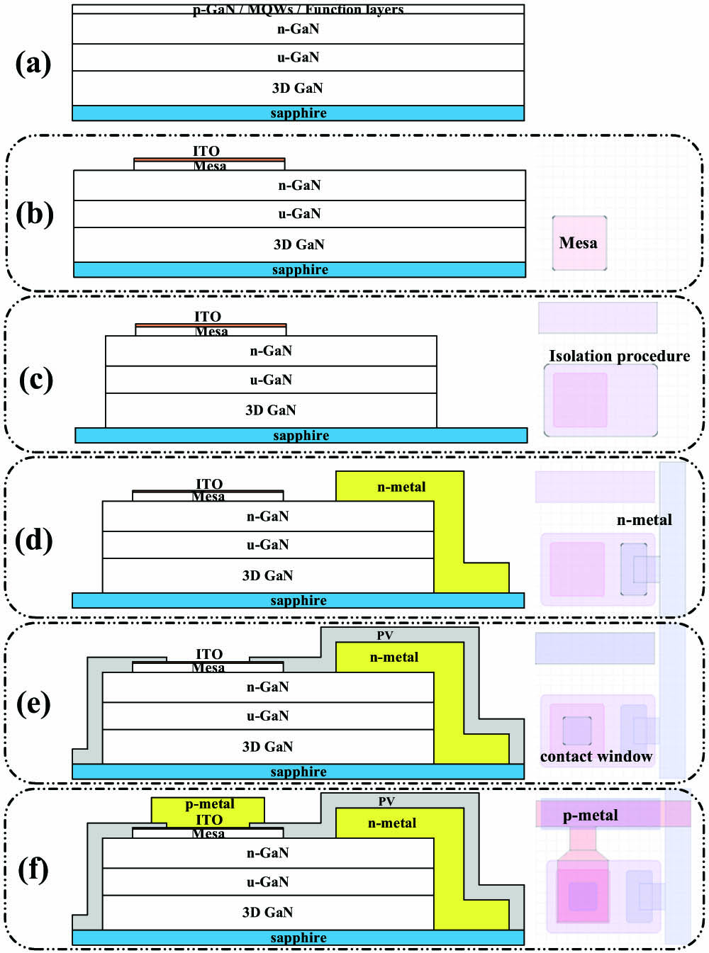
Four-inch commercial sapphire-based blue GaN LED epitaxial wafers were adopted to fabricate our devices. On 600-μm-thick patterned sapphire substrates (PSSs), the epi-layers were grown by using metal organic chemical vapor deposition (MOCVD) and primarily consisted of a 2-μm-thick 3D-GaN, a 2-μm-thick u-GaN, and a 4.5-μm-thick multilayer composed of n-GaN, multi-function layers, multi-quantum-wells (MQWs), and p-GaN.
As shown in Fig. 1, with a 5-step lithography process, bottom-emitting monolithic micro-LED arrays driven by a passive matrix were fabricated. We first deposited a 75-nm-thick indium tin oxide (ITO) layer on the p-GaN. In the first step, we defined both the ITO current spreading region and the GaN mesa altogether (self-alignment) by a 2-step etching process composed of ITO wet etching in a and HCl mixture, followed by inductively coupled plasma reactive ion etching (ICP-RIE) of GaN using the same photoresist mask (PM). In the second step, ICP-RIE was used again for a deeper etching [Fig. 1(c)] to isolate all the pixels. In the third step, n-electrodes (2200-nm-thick Cr/Al/Ti/Pt/Au) were patterned on the samples with a standard lift-off process using negative photoresist, followed by 10 min annealing at 250°C in , and consequently, column lines of the PM structure were formed. In the fourth step, contact windows for p-type injection were opened with ICP-RIE after the deposition of a passivation (PV) layer (1000 nm ). In the fifth step, p-electrodes were patterned with the same metal lift-off and annealing as before. Row lines and finger pads for further flexible printed circuit (FPC) bonding were thus formed. Finally, the sapphire substrate was thinned to 300 μm with chemical mechanical polishing (CMP), and the wafer was diced into six dice. Each die, comprising a micro-LED array with a specific mesa dimension, was connected to a pre-developed peripheral circuit through an FPC.
Figure 1.Process flow of the 5-step lithography for the micro-LED displays. The left side is the side view and the right side is the top view. The figure is not drawn to scale. (a) The initial state of the epi-wafer, (b) the current spreading region and mesa fabrication, (c) the pixel isolation, (d) the n-contact metal deposition, (e) the p-contact window formation, and (f) the p-contact metal deposition.
Details of the as-fabricated micro-LED device can be seen from the optical micrographs illustrated in Fig. 2. All micro-LEDs located in the same column share a common cathode, while those in the same row share a common anode. Hence, each micro-LED is addressable by providing a forward voltage through its corresponding line and row [24]. To reduce the interconnect resistance, thick multi-layer metals were employed. In that case, metal wire breaking is prone to occur at the row and column crossing points. Thus, the semiconductor right beneath the row lines was preserved from the etching in order to lift up the rows so that they match the height of the columns better. In Fig. 2, the row lines appear seemingly discrete, and the column metals look much darker, as they are of a lower altitude (deposited directly on the PSS). This interconnect layout design reduces the altitude difference between the row and column metal lines, effectively reducing the risk of broken metal lines and the insulation layer () at the intersections.
Figure 2.Microscopic photograph of a μ micro-LED array with one pixel turned on and an enlarged view of an active pixel picked out from the micro-LED arrays with mesas ranging from μ to μ.
A matrix of micro-LEDs was built for display study, as shown in Fig. 3. The as-fabricated micro-LED arrays are available to display both characters and pictures pixel by pixel after being connected to a pre-developed peripheral circuit. A micro-LED array with a mesa size of 50 μm displaying the Chinese characters “Fuzhou University” and the English characters “Micro LED” is shown in Fig. 3.
Figure 3.Images of the 50 μm micro-LED array () in operation. Both Chinese characters and English characters are shown in the display.
The measurements of the current-voltage-luminance (I-V-L) characteristics under the DC operation were first conducted to get a fundamental understanding of the as-fabricated micro-LED devices. Based on both statistical and photometrical measurement considerations, a cluster of pixel arrays from each type of micro-LED devices was selected for measurement [shown in Fig. 4(d), where the white dotted box refers to the entire micro-LED array]. A synchronous I-V-L test was carried out with a multifunctional integration luminescent device test system (D3000-16CH) composed of a high-voltage source-measurement unit and a TOPCON integrated spectroradiometer SR-3A.
Figure 4.I-V-L characterization of the micro-LED arrays based on the measurement of a clustered pixel array. (a) The I-V characteristics of the micro-LED arrays. The upper inset shows the photograph of the micro-LED arrays in full operation under 3 V bias. (b) The luminance as a function of current density of the micro-LED arrays. The upper inset shows the photos taken during the measurement. The lower inset plots the relation between the luminance of one single LED pixel (in different sizes) and the current density. (c) The EQE as a function of current density of the micro-LED arrays. The inset is the same curves plotted in a semi-log scale. (d) The selected cluster of pixel array in each micro-LED device as the data source.
Typical diode characteristics with mesa size dependence are seen in Fig. 4(a). Micro-LEDs with a larger mesa size generate a higher current under the same voltage, yet micro-LED arrays with smaller mesa dimensions withstand higher current densities. Indeed, with a higher surface-to-volume ratio, a smaller micro-LED is recognized to have less current crowding as well as better heat dissipation capability [30,31].
Figure 4(b) plots the luminance characteristic curves as a function of the injection current over different micro-LED arrays. As the insert shows, a measurement field with a diameter of 1000 μm, which is several times larger than the pixel pitch of the micro-LED arrays (i.e., 300 μm), was applied to collect the light from the selected pixel array with a 0.2° solid angle emission upon the sapphire side. Consequently, spectrum information was obtained, based on which the luminance as well as the EQE was calculated. With the largest emitting area, the μ micro-LED array exhibits the highest luminance of nearly . The μ micro-LED array exhibits a peak luminance of only slightly more than . This notwithstanding, a luminance of at the maximum efficiency of the μ device has been observed, much higher than the luminance (at maximal EQE) reported earlier [24–26]. Because the area used to calculate luminance includes the region between the pixels, the luminance can be increased just by reducing the pixel pitch. For device study, it is more convenient to have the luminance calculated only from the emitting regions, which we define as “brightness” in this paper, just to remove the influence from different aperture ratios between the emitting areas and pixel areas. The single micro-LED brightness as a function of mesa size is shown in the insert semi-log plot in Fig. 4(b). At low current density (phase 1), where most carriers are injected smoothly into the active region, the brightness of a small micro-LED is as good as that of a large device. The evolving slopes are also almost equally large. At high current density, curves of smaller LEDs have a lower slope than the low current density case. (Note that large devices cannot withstand high current densities due to current crowding, and hence they have no data.) This is because the carrier dynamics is in the second phase, where defects play a significant role. Smaller micro-LEDs possess more sidewall related defects (in relative terms) and higher non-radiative recombination rates, and thus the slopes decline to a greater extent. As the current density is increased even further (phase 3) where most defect related traps are filled, an approximately linear increase in the amount of the output photons would occur.
An EQE analysis helps us get a deeper insight. The EQE is defined as where and are the rate of emitted photons and injected electrons, respectively. Assuming a non-Lambert reflector of the light shape distribution emitted by the micro-LED array, with luminance , Eq. (1) can be calculated as where , , , , , , , , and are the active pixels number, the pixel pitch, the charge of an electron, the Planck’s constant, the velocity of light, the forward current, the wavelength, the relative electroluminescence (EL) intensity, and the luminosity function provided by the Commission International de l’Eclairage chromaticity (CIE), respectively.
The EQE as a function of the current density is plotted in Fig. 4(c) based on the formula above. Consistent with the carrier dynamics discussed earlier, the EQEs first go up and then down. Maxima of the EQE can be found from the insert logarithmic scale plot, where larger micro-LEDs exhibit higher maxima at lower current densities. This can be explained by the different weights between the non-radiative Shockley–Read–Hall (SRH) recombination rate and the radiative recombination rate that resulted from the variation of surface-to-volume ratio over different micro-LED arrays. The μ micro-LED array, with minimum sidewall defects in relative term, naturally has the highest maximum EQE value ( at current density and luminance). The μ micro-LED array exhibits a maximum EQE of 12.13% at and . Such a small drop in EQE is acceptable, as future optimization based on better heat management along with higher light extraction efficiency (LEE) in small LEDs may compensate for this drop [30,41,42]. After peak EQEs are reached in Fig. 4(c), all curves exhibit a dramatic decline and finally overlap together. At this stage, the radiative recombination continuously increases with the current density, and the non-radiative SRH recombination centers are mostly saturated, but another factor, i.e., the current crowding, starts to be serious and dominates the performance. The curve down bending occurs earlier for larger micro-LEDs, as they are more prone to current crowding.
As mentioned previously, micro-LED displays typically operate in a pulse mode. We then investigate the transient behaviors of micro-LED arrays under pulsed excitations. As the schematic diagram in Fig. 5(a) shows, our micro-LED pixel array device connected in a series with a 10 Ω resistor was driven by a pulse voltage from a signal generator, where a high-sensitivity photomultiplier tube (PMT) was employed to measure the emitting light (EL) intensity and investigate the temporal response characteristics. A relatively long-duration-pulsed signal (i.e., 100 kHz frequency, 50% duty cycle) was applied in Fig. 5(c). The electroluminescence (EL) intensity from the micro-LED array measured by the PMT and the voltage on the series resistor were both collected by a multichannel oscilloscope.
Figure 5.(a) Schematic diagram of the transient characteristic measurement system. (b) The typical response of a micro-LED to a pulse excitation. (c) The 100 kHz pulse signal with 50% duty cycle and voltage varied from 2.75 to 3.25 V. (d)–(f) The normalized EL intensity of the micro-LED arrays as a function of time under 100 kHz pulse operation with applied voltage from 2.75 to 3.25 V. (The μ micro-LED array under 3.25 V bias excitation is undermeasured due to the output limit of the pulse signal generator.)
Generally, the response of a micro-LED to a pulse voltage excitation can be divided into three steps: rising, stabilizing, and falling [Fig. 5(b)]. The rise time () is defined by the time interval between the 10% and 90% points of the stable signal. As shown in Figs. 5(d)–5(f), where transient EL intensity curves over different micro-LED arrays were normalized for a better comparison, smaller micro-LEDs reach the peak brightness faster than the larger ones. Table 1 lists the rise time of the micro-LED arrays. Micro-LED arrays with mesa sizes smaller than 50 μm exhibit a significantly faster response under the pulsed excitations.
Response Speed of the Micro-LED Arrays
Mesa Size
(ns)
2.75 V
3.00 V
3.25 V
μ
35
32.8
32
μ
40.6
39.5
37.8
μ
41.8
44
43.9
μ
65
51.8
48
μ
136.5
65
52.5
μ
173.5
125
The micro-LED photon intensity response time is mainly affected by two factors: the carrier lifetime and the resistance-capacitance (RC) constant. The latter can be estimated by where , , , , , and are the resistivity, thickness, area, dielectric constant, electric field, and current density across the micro-LED active region, respectively. As illustrated in Fig. 4(a), the upper inset, smaller micro-LEDs can provide higher current densities. Calculations based on Eq. (3) indicate that the RC constants of the arrays are in the order of ns for the micro-LED size under 100 μm, with the applied voltage of 2.75–3.5 V and current density in the range of a few 10s to . Therefore, the measured rise time is mainly determined by the carrier lifetime. As the measured also includes the intrinsic RC time constant of the instrument, the actual response time should be shorter than the measured data shown in Fig. 5.
Interestingly, a closer look at Figs. 5(d)–5(f) reveals overshoots in the normalized micro-LED EL intensity. We found that the overshoots only occurred when the current density exceeds a specific value. In this situation, the normalized EL intensity reached its maximum, followed by a small oscillation until a stable value was reached. The difference between the overshoot peak and the value of the steady state was larger in the smaller micro-LEDs. Consequently, it can be concluded that, for micro-LEDs, the injection and recombination processes are both size- and time-dependent. In the initial stage of the injection, carriers access the active area smoothly. The photons generated by the MQW reach a maximum number after the rising period, seen as the overshoot peak in Figs. 5(d)–5(f). Soon after, the non-radiative recombination that is mainly due to the defective sidewalls also occurs, and the space-charge field created by those carriers trapped in the defects will hinder the subsequent carrier injection flow by virtue of the Coulombic repulsive force. As a result, the light outputs of the micro-LED array exhibit a decline. Eventually, in the third phase, the forward field and the defect-induced space-charge field reach an equilibrium state. A steady current flows across the device, and the EL intensity reaches a stable value. This mechanism is related to the sidewall defects and is more pronounced when the micro-LED size gets smaller. With a better current spreading and a higher surface-to-volume ratio, carriers in the smaller micro-LEDs are more likely to reach the mesa edge and finally be captured by the sidewall defects. Such a process does not reach equilibrium instantaneously, meaning it requires time ( based on our results) for the electrons to be captured by the defect traps.
Therefore, the 7 μm micro-LEDs, with the maximal surface-to-volume ratio, exhibit the maximal difference between the overshoot peak and the stable value. In addition, the overshoots occur at an initial 100 ns after applying voltage on the 7 μm micro-LED arrays. As a result, an applied voltage pulse with an order of 100 ns can operate mostly in the overshoot part of the transient response of the micro-LED arrays, which can significantly affect the performance of the micro-LED arrays in a positive manner. The EL intensity of the μ device array, as a function of time under the 1 MHz pulse operation, is plotted in Fig. 6. The EL intensity under the DC operation was also measured and used as a baseline value (see arrows in Fig. 6). We find that the transient behavior at 1 MHz is qualitatively similar to those at 100 kHz in Fig. 6, and the EL intensity curves with longer pulse durations are the natural extension of the short duration ones with no additional features. In Fig. 6, after the initial overshoot, the EL intensity eventually reaches a stable value, i.e., the DC baseline, and finally gets down to zero when the input pulse ends. For 10% and 20% duty ratios, there is simply no time for the voltage to stabilize at the baseline plateau before the signal disappears. For the three voltages tested in the 7 μm devices, the smaller the voltage, the lower the DC output baseline. However, the main message of Fig. 6 is that, as long as the duty cycle is short enough, the baseline does not matter anymore, since the overshoot dominates. Thus, smaller micro-LEDs possess a high potential for operating at applied voltage pulses with very short time durations.
Figure 6.EL intensity of the μ device array as a function of time under 1 MHz pulse operation. (a) 2.75 V, (b) 3.00 V, and (c) 3.25 V.
On the above basis, a luminance loss mechanism under high-frequency-pulsed excitation is deduced, i.e., the longer the rise time, the greater the luminance loss compared with the DC case. Moreover, it can be well expected that, when further reducing the pulse width, where the overshoot is large enough to overcompensate the luminance loss in the rising and falling period, an enhanced performance of the micro-LED arrays would be observed. Figure 7 plots the normalized luminance as a function of the current density, which was calculated by dividing the pulse luminance () by the DC luminance (),
Figure 7.Normalized luminance as a function of the duty cycle with various forward voltages and frequencies.
Theoretically, the normalized luminance defined in this way should equal the duty cycle. Experiment results agree well with the analyses. For pulsed frequency , where luminance loss induced by the rising and falling period is negligible, all micro-LED arrays exhibit a normalized luminance close to the theoretical value. Nevertheless, at high frequency, the normalized luminance falls below the theoretical values, a trend that is more pronounced with the mesas increasing from μ to μ. This gap widens further at the decreasing duty cycle and forward voltage. Exceptionally, the μ micro-LED array does not have this gap, which even exhibits a normalized luminance higher than the theoretical value under 2.75 V. In these cases, overshoots dominate the performance of the μ micro-LED array, as illustrated in Fig. 6. Efficiency drop induced by the sidewall defects has not fully taken the effect.
A similar scenario can be obtained in the EQE analysis at a high frequency. Assuming the same spectral distribution as the DC case, the EQE under the pulse operation can then be estimated by Eq. (2). Figure 8 plots the EQE at 1 MHz and various duty cycles. Except in the 7 μm case, the EQE increases with the duty cycle. Again, three input voltages are chosen (2.75 V, 3.00 V, and 3.25 V), which are roughly on the left, middle, and right of the maximum EQE point, according to the DC operation [Fig. 4(c)]. For all the three voltages, the 7 μm micro-LED array is seen to outperform other devices for small duty cycles, especially at 10%. For instance, Fig. 8(a) shows an for all the duty ratios, whereas other micro-LED arrays exhibit variable degrees of EQE decline upon the reduction of the duty cycle. At the 10% duty cycle, the μ micro-LED array shows the highest EQE of 12.05%. On the other hand, the 100 μm devices are really not suitable under this operation condition. At duty cycles , it is far less efficient compared to the others.
Figure 8.Estimated EQE under different pulse operations with 1 MHz frequency and various duty cycles. (a) 2.75 V, (b) 3.00 V, and (c) 3.25 V.
It is evident that the fast response speed along with the overshoot mechanism enables the μ micro-LED array (small-sized micro-LEDs) to operate at a high frequency with a pulse width in the order of 100 ns. By employing the short-pulse operation mode, such brightness boosting effect can be applied in a real display. This can be achieved by using scrambled pulse width modulation (S-PWM) or dispersed PWM techniques [43], where a single original pulse in each subfield is split into several sub-pulses with the same total time of applied voltage [as shown in Fig. 9(a)]. For a conventional LED display, the luminance is determined by the time span of the applied voltage. For the short-pulse operation mode, however, the luminance is determined by the number of short pulses. Each pulse in the order of 100 ns delivers a constant pulse of light. The number of pulses in a time frame, e.g., 16.7 ms for 60 Hz display, will determine the luminance level (or gray scale) of a display.
Figure 9.(a) Conventional PWM mode compared with short-pulse PWM mode. (b) The relative luminance of a 7 μm micro-LED generated within a 100 ns duration. (c) The short-pulse mode combined with overshootings.
Based on the experiment results of our micro-LEDs, the peaked brightness at the initial shows a higher value compared to the steady state. Therefore, it can be well expected that, by taking advantage of the overshoot mechanism, the total turn-on voltage time for achieving the same level of brightness at short pulse operation mode is less than the conventional operation mode by using continuous voltage. Consequently, lower power consumption can be expected since a smaller total duty ratio of the voltage pulse would be applied. As shown in Fig. 9(b), the relative luminance of the 7 μm micro-LED generated within a 100 ns duration pulse can be estimated by integrating the corresponding EL intensity curve. Thereby, under 2.75 V pulse excitation, a 25.5% luminous enhancement of the 100 ns short pulse is acquired, compared with that upon the steady state. Based on this argument, for a frame time [as illustrated in Fig. 9(c)], the short-pulse PWM mode can deliver a 25.5% higher luminance, compared with the conventional PWM mode.
4. CONCLUSION
We have studied both the size and temporal dependence of GaN micro-LED arrays. The luminance and EQE of micro-LED arrays are found to be varied by the mesa size ranging from 7 to 100 μm. Under the DC operation, the luminance and EQE decrease with the reduction of the mesa size. In contrast, micro-LED arrays with smaller mesa dimensions are observed with higher luminance and EQE under a 1 MHz pulse operation and a short duty cycle. Reducing the pulse duration to 100 ns, the 7 μm devices demonstrate a 20% increase in EQE compared to the DC case. A hypothesis based on carrier injection/recombination and trap filling dynamics is used to explain the effect. The efficiency drop in small micro-LEDs may be drastically reduced by applying voltages of very short pulses, in the order of 100 ns. Small sized micro-LEDs thus possess a very high potential for next-generation displays.
Acknowledgment
Acknowledgment. We also thank local government funding for Rich Sense Electronics Technology Inc.
[37] Q. Yan. Micro-LED driving the third wave of technology revolution of information display. Proceedings of the International Display Workshops, 25, 2-3(2018).
Junyang Nie, Zhi Zhang, Kongjie Chen, Yifeng Liu, Shuang He, Zhonghang Huang, Xiaoning Zhang, Jie Sun, Fan Zhang, Yongsheng Wu, Qun Yan, "Systematic study on size and temporal dependence of micro-LED arrays for display applications," Photonics Res. 11, 549 (2023)