Polarization control is at the heart of high-capacity data optical communication systems, such as polarization-division multiplexers and Stokes vector modulation transmitters. Despite passive polarization control being mature, the realization of monolithically integrated polarization controllers and single longitudinal mode light sources, such as distributed-feedback (DFB) lasers, is of importance. In this research, we report an AlGaInAs multiple-quantum-well photonic integrated circuit device which can control the state of polarization of the output light source, consisting of a polarization mode converter (PMC), a differential phase shifter (DPS), and a sidewall grating DFB laser. We demonstrate an asymmetrical stepped-height ridge waveguide PMC to realize TE to TM polarization conversion and a symmetrical straight waveguide DPS to enable polarization rotation from approximately counterclockwise circular polarization to linear polarization. Based on the identical epitaxial layer scheme, all the PMC, DPS, and DFB lasers can be integrated monolithically using only a single step of metalorganic vapor-phase epitaxy and two steps of III-V material dry etching. For the DFB-PMC device, a high TE to TM polarization conversion efficiency (98.4%) over a wide range of DFB injection currents is reported at 1555 nm wavelength. For the DFB-PMC-DPS device, a nearly 60° rotation of the Stokes vector on the Poincaré sphere was obtained with a range of bias voltage from 0 to at a laser drive current of 170 mA.
1. INTRODUCTION
The ability to control the polarization state is of substantial interest in optical communication systems such as those using high-speed complex digital signal processing to manipulate the TE-TM polarization state of light [1] or Stokes vector modulation and direct detection systems [2,3]. For these applications, there is a growing interest in integrating a polarization controller with the light source, the detectors, and other components in a photonic integrated circuit (PIC). As an increasing number of devices such as laser diodes (LDs) [4] and electro-absorption modulators [5] utilize multiple-quantum-well (MQW) structures as the active region, it is desirable to design a polarization controller compatible with MQW structures.
Several different material systems and designs have been proposed for polarization controllers including the silicon-on-insulator platform [6], the InGaAlAs/InP platform [5], and the InGaAsP/InP platform [7,8]. A typical waveguide polarization convertor comprises a cascade of polarization mode converters (PMCs) and MQW polarization-dependent phase shifters (PD-PSs) [5,9] to achieve an arbitrary state of polarization (SOP). The light source can be an external LD or a monolithically integrated laser [4,10]. However, many reported PMCs utilize bulk material as the core layer in the waveguide to achieve a high polarization conversion efficiency (PCE) at a short waveguide length. This approach requires relatively complicated regrown butt-joint PIC techniques to integrate a bulk PMC with an MQW-based PD-PS. In Ref. [9], a passive bulk PMC was monolithically integrated with an active MQW-based PD-PS by using the butt-joint technique and was a demonstrator of an efficient polarization controller in the InGaAsP/InP material system; however, the device had no monolithic LD. In Ref. [3], an MQW-based PMC was monolithically integrated with an MQW-based Fabry–Perot (FP) LD using the identical epitaxial layer (IEL) integration scheme, but the PCE was limited, being only 80% in Refs. [4,11] and around 50%–68% in Ref. [9]. Until now there is no report of a PMC integrated with a distributed-feedback (DFB) laser.
The crucial issue for integrating PMCs with MQW devices is the inherent birefringence of the MQW, which disturbs the optimal rotation of the SOP. The two main mechanisms of SOP conversion are the mode-evolution method [12], which utilizes the shifting of the propagating mode inside the waveguide, and the mode coupling method [8], which exploits the beating between two eigenmodes to enable polarization rotation along the PMC waveguide. Because mode coupling PMCs enable polarization conversion within a short length of waveguide, it is important to reduce the absorption loss caused by the inter-band exciton transitions inside an MQW-based PMC monolithically integrated with an MQW-based LD [13]. To realize good mode-matching between the waveguides of monolithic PMCs and LDs, we have proposed an AlGaInAs/InP MQW-based sidewall grating (SWG) DFB laser monolithically integrated with a stepped height waveguide PMC [14]. A novel MQW-based epitaxial structure was designed and optimized for both the PMC and SWG DFB laser through a series of full-wave simulations. In this work, based on our simulation work an AlGaInAs MQW SWG DFB laser was fabricated and monolithically integrated with both a stepped waveguide PMC and a differential phase shifter (DPS) based on the IEL integration scheme, for the first time. This approach needs only a single step of metalorganic vapor-phase epitaxy (MOVPE) and two steps of III-V material dry etching. The monolithic DFB-PMC and DFB-PMC-DPS devices reported here avoid the complicated etch and regrowth processes required for conventional buried grating DFB laser structures and time-consuming butt-joint or selective area growth PIC technologies. The DFB-PMC device has a high TE to TM PCE (98.4%) over a wide range of DFB injection currents () at an operating wavelength of 1555 nm. For the DFB-PMC-DPS device, a rotation of nearly 60° of the Stokes vector (SV) was obtained on the Poincaré sphere with a range of bias voltage from 0 to and .
Sign up for Photonics Research TOC. Get the latest issue of Photonics Research delivered right to you!Sign up now
2. DEVICE DESIGN AND FABRICATION
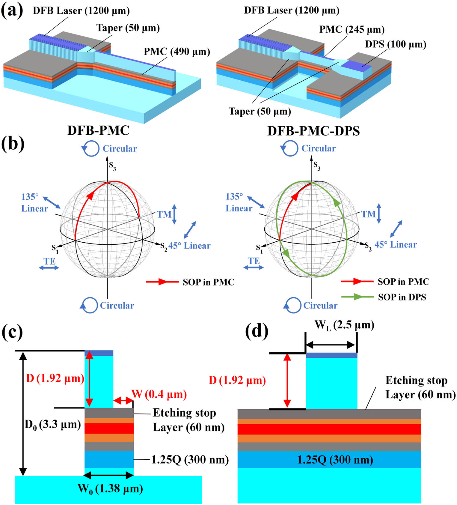
The wafer structure used for the DFB-PMC and DFB-PMC-DPS is the same as that described in Ref. [14]. The wafer was grown on an InP substrate by MOVPE. The room temperature photoluminescence (PL) peak of the QWs was located at a wavelength of 1530 nm. An optimized 300 nm thick 1.25Q layer (1.25Q means the room temperature PL peak of this material is at 1.25 μm) is embedded below the MQW to increase the difference between the propagation constants of the and fundamental transverse modes of the PMC to reduce the half-beat length () and increase the PCE. The optical confinement factor of the QWs is 9%. Two kinds of polarization controllers—DFB-PMC and DFB-PMC-DPS—are proposed and are shown in Fig. 1(a). Both devices contain the same 1200 μm long SWG ridge DFB laser. The ridge waveguide of DFB is 2.5 μm wide and 1.92 μm high. The gratings are of first order with a 50% duty cycle, formed by etching 0.6 μm depth into the sidewalls of the waveguide, as shown in Fig. 1(a). For the DFB-PMC device, LDs with three different Bragg wavelengths were designed and fabricated. The grating period is 238 nm for a 1550 nm Bragg wavelength, 236.5 nm for a 1540 nm Bragg wavelength, and 240.3 nm for a 1565 nm Bragg wavelength. A quarter-wavelength shift section was inserted at the center of the DFB laser cavity to ensure single longitudinal mode (SLM) oscillation. The lengths of the PMCs in the DFB-PMC and DFB-PMC-DPS are 490 μm and 245 μm, respectively. The PMC is connected to the DFB LD using a 50 μm long taper for the DFB-PMC device and is connected to the DFB laser and DPS, respectively, by two 50 μm long tapers for the DFB-PMC-DPS device. The width of the taper is changed from 2.5 to 1.38 μm to facilitate the TE mode transition to the PMC and prevent the generation of multiple transverse modes. The simulated reflection coefficient between the shallow etched DFB and deeply etched taper sections is about , which has a negligible effect on the DFB performance. The simulated taper excess optical loss is 1%, i.e., 0.044 dB, which includes the scattering and mode mismatch loss and can also be neglected. Figure 1(b) presents the SV rotation inside those two devices. For the DFB-PMC device, the SV rotates around the axis arriving at the plane where the output mode is TM-polarized. For the DFB-PMC-DPS device, after the PMC, the SV rotates around the axis (red line) close to the north pole, corresponding to counterclockwise circular polarization. The SV is then rotated around the axis within the plane by using the reverse biased DPS section (green line). Assuming a TE-polarized input [], the variation of and the PCE inside the PMC waveguide can be found from [15,16] where is the rotated angle of the eigenmodes in the PMC waveguide, and is the length of the PMC. In this work is equal to the half-beat length , where and are the propagation constants of the and eigenmodes in the PMC waveguide. To realize the SV rotation in Fig. 1(b), the value of should be 45° and should be equal to for the DFB-PMC and equal to for the DFB-PMC-DPS. The dimensions of the stepped-height PMC waveguide chosen here are μ, μ, μ, and μ, as shown in Fig. 1(c). can be precisely controlled because the top 60 nm thick AlGaInAs waveguide layer acts as a dry etch stop layer when using a inductively coupled plasma (ICP) recipe. Figure 1(d) presents the cross section of the DPS, which is a symmetric, shallow etched ridge waveguide with a width of 2.5 μm and height of 1.92 μm, the same as that of the DFB section. Figures 2(a) and 2(b) present the fundamental mode profiles in the taper output section and PMC waveguide. The PMC eigenmode is optimized to rotate the electric/magnetic fields through 45°. After propagating a half-beat length , the SV is rotated 180° around the axis as found from Eq. (1), and the output becomes purely TM-polarized. Hence, to optimize the PCE and of the PMC waveguide, a full-wave simulation was made using an FDTD software package. The input light wavelength was set at 1550 nm. The calculated effective modal indices () of the fundamental TE and TM modes are 3.21109 and 3.20951, respectively. Figures 2(c) and 2(d) show contour plots of the calculated PCE and as a function of and at the operating wavelength of 1550 nm. The final optimum widths of the PMC waveguide are μ and μ, which provide a high PCE (97.3%) and short (490 μm).
Figure 1.(a) Schematic of the monolithic DFB-PMC device (left) and DFB-PMC-DPS device (right); (b) SV propagates inside the DFB-PMC (left) and the DFB-PMC-DPS device (right); (c) cross-section structure of the PMC; (d) cross-section structure of the DPS.
Figure 2.(a), (b) The fundamental eigenmodes in taper output (a) and PMC stepped-height ridge waveguide (b); (c) and (d) calculated maximum PCE (c), and corresponding (d) as a function of waveguide width () and corner width () at an operating wavelength of 1550 nm.
In the DPS waveguide, via the band-filling effect (forward bias) or quantum-confined Stark effect (QCSE) (reverse bias), the phase shift between mode and mode in the DPS can be tuned because the phase modulation efficiency generally differs for the and modes. The SV rotation angle in the DPS can therefore be controlled by the bias voltage [15]. DPSs based on the QCSE have picosecond switching speeds and are faster than those based on the band-filling effect which have nanosecond switching speeds [17], although measurement of the switching speed is beyond the scope of this paper. Reverse bias operation of the DPS is therefore preferred and was used to change the rotation angle , which can be calculated from where and are the changes of the refractive index of the and modes, respectively, and are determined from the change in absorption coefficient () using the Kramers–Krönig relationship [18]: where is the photon energy, is Planck’s constant divided by , and the total absorption coefficient, , is the sum of the absorption coefficient of the exciton resonance in the quantum well () and the absorption coefficient between the conduction and valence band transition (). They are expressed as [19] ⏧⏧⏧⏧where and are the envelope wave functions of conduction and valence bands, respectively, is the refractive index, is the velocity of light in vacuum, is the permittivity of free space, and is the as-grown QW width. is the Sommerfeld enhancement factor, is the Lorentzian broadening factor, and is the optical matrix element at the band edge. The parameters used here to calculate are referenced in Ref. [20]. Figure 3(a) shows the calculated TE and TM absorption coefficients as a function of wavelength with at 0 V and , respectively. The modal absorption coefficient for the TE mode at 1.55 μm wavelength is about and the TM mode absorption coefficient is at 0 V bias voltage. The TE modal absorption coefficient of fits very well with our measured result of , as discussed in Section 3. As is increased, there is a redshift of the exciton peak. It is also found that the absorption coefficient at bias voltage is high (), which means the DPS cannot be too long. Here a 100 μm length DPS was used, and 22 dB absorption loss at bias was produced, the same as the measured one. Figure 3(b) presents the difference of the effective refractive index changes between the TE and TM modes () for different . The calculated as a function of at 1.557 μm wavelength is presented in Fig. 3(c), with a predicted 71° phase shift at .
Figure 3.(a) Calculated TE and TM absorption coefficients in the DPS. (b) The difference of the effective refractive index changes between the TE and TM modes at different . (c) Phase-shifted angle as a function of at 1.557 μm operation wavelength.
The DFB-PMC device fabrication processes are presented in Fig. 4. The wafer was grown on an InP substrate by MOVPE [Fig. 4(a)]. The DFB grating and PMC first step waveguide pattern were defined by electron-beam lithography (EBL). Negative tone hydrogen silsesquioxane (HSQ) was used as the EBL resist hard mask for ICP dry etching, as shown in Fig. 4(b). Figure 4(c) shows the shallow etched ridge, which took place in two stages. The ridge was first etched to a depth of 1.89 μm in an ICP dry etch tool using a gas mixture, the average etch rate for InP and InGaAsP being about 183 nm/min, and then the gas recipe was changed to , to etch the ridge to a final depth of 1.92 μm. This could be stopped on the AlGaInAs layer, as the average etch rate of InP/InGaAsP was about 78 nm/min, and that of AlGaInAs was 3 nm/s, achieving 26-fold selectivity. After the shallow etch, both the DFB section and the top and one side of the PMC were protected by HSQ defined by EBL, as shown in Fig. 4(d). A second stage of etching was then used to etch one side of the PMC waveguide to a depth of 3.3 μm [Fig. 4(e)]. Finally, all HSQ was removed by HF acid, as shown in Fig. 4(f). The fabrication workflow is depicted in Fig. 4(g); only a single step of MOVPE and two steps of III-V material dry etching are required for the whole integrated device. Scanning electron microscope (SEM) images of the PMC waveguide after the first shallow etch, second step EBL, and deep etch are shown in Figs. 4(h), 4(i), and 4(j), respectively. The subsequent deposition of and HSQ passivation layers, window opening, P-contact deposition, substrate thinning, and N-contact deposition were the same as for conventional LD fabrication [21]. SEM images of the DFB grating, output facet of the PMC, and DFB-PMC device are presented in Figs. 5(a)–5(c). The optical microscope pictures of the completed DFB-PMC and DFB-PMC-DPS devices are depicted in Figs. 5(d) and 5(e), respectively. Finally, the devices were mounted epilayer up on a copper heat sink on a Peltier cooler. The heat sink temperature was set at 20°C and the devices were tested under CW conditions.
Figure 4.(a)–(f) Fabrication procedures: (a) MOVPE epilayer growth, (b) EBL to define the laser and PMC first step waveguide, (c) ICP shallow etching, (d) EBL to define the second step waveguide of the PMC, (e) ICP deep etching, (f) HSQ elimination. (g) Workflow of monolithic DFB-PMC device fabrication. (h)–(j) SEM images after (h) the first shallow etch, (i) second step EBL using HSQ photoresist, (j) PMC deep etch and HSQ elimination.
Figure 5.(a)–(c) SEM images of (a) the DFB laser with sidewall gratings, (b) output facet of the PMC, (c) DFB-PMC device. (d) and (e) Microscope pictures of the (d) DFB-PMC device and (e) DFB-PMC-DPS device.
For the DFB-PMC-DPS device, the fabrication process is the same as that of the DFB-PMC devices and will not be discussed in further detail.
3. DEVICE MEASUREMENT
A. DFB-PMC Device
As described above, for the DFB-PMC device, DFBs were fabricated with three Bragg wavelengths, i.e., 1540, 1550, and 1565 nm. Figure 6 shows their optical spectra at specific injection DFB currents () and 2D optical spectra as a function of from the DFB rear side and PMC side, respectively. All spectra were measured with a resolution bandwidth of 0.06 nm. The measurement results of wavelength, single-mode suppression ratios (SMSRs), and average current-induced wavelength redshift coefficient (ACWRC) are listed in Table 1. The measured wavelengths of the DFB lasers with designed operation wavelengths of 1540 nm, 1550 nm, and 1565 nm are 1543.6 nm, 1555.8 nm, and 1568.2 nm, with set at 150 mA, 170 mA, and 170 mA, respectively. Compared to the designed Bragg wavelengths, the measured wavelengths are slightly redshifted due to the heating effect. The corresponding SMSRs measured from the DFB rear facet are 27 dB, 29 dB, and 38 dB, respectively. At the PMC output facet, the SMSRs were reduced to 8 dB, 12 dB, and 20 dB. This is due to the significant inter-band and exciton absorption inside the PMC waveguide when the propagating light wavelength is close to the PL wavelength (1530 nm) of the MQW core. The measured ACWRCs from the DFB and PMC sides are 0.025 nm/mA, 0.0207 nm/mA, and 0.0271 nm/mA for Bragg grating wavelengths at 1540 nm, 1550 nm, and 1565 nm, respectively, all exhibiting stable SLM operation. To estimate the internal loss in the PMC waveguide, an 800 μm length FP laser was fabricated in the same wafer and fabrication run, and the internal loss in the waveguide was measured by the Haki–Paoli method [shown in Fig. 7(a)]. To estimate the value of the DFB lasers, an 800 μm long DFB laser with a Bragg wavelength of 1565 nm and a -phase shift section inserted at the center of the cavity was also fabricated. Figure 7(b) shows the optical spectrum at the threshold current (48 mA). The measured central wavelength is 1566.5 nm, and the stop band width () is 1.14 nm. The grating coupling coefficient can be estimated using [22] where is the effective index (3.26); is the lasing wavelength of the DFB laser. The of the fabricated grating is estimated to be , and for the 1200 μm length DFB laser, which ensures stable SLM operation.
Measured Parameters of the Three DFB-PMC Devices with Different Designed Bragg Wavelengths
Designed Bragg Grating Wavelength (nm)
DFB Facet SMSR (dB)
PMC Facet SMSR (dB)
Measured Current (mA) and Wavelength Range (nm)
ACWRC (nm/mA)
1540
27
8
Current: 118–170
0.0250
Wavelength: 1542.9–1544.2
1550
29
12
Current: 104–220
0.0207
Wavelength: 1554.2–1556.6
1565
38
20
Current: 97–211
0.0271
Wavelength: 1566.3–1569.4
Figure 6.(a)–(d) Measured optical spectra for the 1543 nm DFB-PMC device measured from DFB (a), (b) and PMC (c), (d) facets. (e)–(h) Optical spectra for the 1555 nm DFB-PMC device from DFB (e), (f) and PMC (g), (h) facets. (i)–(l) Optical spectra for the 1567 nm DFB-PMC device from DFB (i), (j) and PMC (k), (l) facets.
Figure 7.(a) Measured net modal gain as a function of the wavelength using the Haki–Paoli method, (b) optical spectrum at threshold current (48 mA) of a 800 μm length DFB LD with a -phase shift section inserted at the center of the DFB LD cavity.
The setup for the SOP measurement is shown in Fig. 8. Devices were mounted on a thermoelectric cooler and the temperature was controlled at 20°C as stated previously. The output light from the PMC was coupled into a lensed polarization-maintaining fiber and transmitted to a polarimeter to measure the SOP. Both the current driver and the polarimeter were controlled by a computer through the general-purpose bus interface by LabVIEW software. We first measured the SOP at the DFB laser rear facet at from 104 to 210 mA, and the SV was constant at (0.998, 0.05, 0.04). Figures 9(a)–9(c) present the SV at the PMC facets of DFB-PMC devices with different Bragg wavelengths. The PCE was calculated from Eq. (2) and the values are listed in Table 2. For the DFB-PMC device with a designed Bragg wavelength at 1550 nm, the average parameter was representing a PCE of 98.4% for (corresponding wavelength range 1554.9–1555.9 nm). The maximum PCE was 99.1% measured at . The deviation of the measured PCE is due to the measurement errors caused by the noise of the DC source driving the DFB laser, and environmental influences such as temperature fluctuations and mechanical vibration. For the DFB-PMC device with a designed Bragg wavelength at 1540 nm, the average PCE over the wavelength range from 1543.6 to 1544.2 nm was found to be 93% for and the maximum PCE was found to be 94.3% at . For the DFB-PMC device with a designed Bragg wavelength at 1565 nm, the average PCE was 89.8% over the range and wavelength from 1567.4 to 1568.7 nm. The maximum PCE was 90.5% (at ). Figure 10 presents a comparison between the calculated PCE from the full-wave simulation and the measured average PCE as a function of wavelength. There is very good agreement between the simulated and measured results.
Measured PCE from the PMC Side of the DFB-PMC Devices
Designed DFB Laser Wavelength (nm)
Measured DFB Laser Wavelength (nm)
Current Range (mA)
Average PCE
MAX PCE
1540
1543.6–1544.2
150–170
93.0%
94.3%
1550
1554.9–1555.9
140–190
98.4%
99.1%
1565
1567.4–1568.7
140–190
89.8%
90.5%
Figure 8.Experimental setup for the SOP measurement for DFB-PMC and DFB-PMC-DPS devices.
In light of the performance of the DFB-PMC devices, the DFB-PMC-DPS devices were fabricated with a Bragg grating wavelength at 1550 nm. Figure 11 shows the optical spectra measured from the rear side of the DFB section and from the DPS output section with . The peak lasing wavelength is at 1557.2 nm with an SMSR of 35 dB at the DFB facet for , and the ACWRC is 0.023 nm/mA. We first measured the SV at the DPS output facet with , as shown in Fig. 12(a). The SV lies near (0.05, 0.5, 0.865) for the range of from 160 to 175 mA. This is a small deviation from a pure counterclockwise circular polarization state and is due to the birefringence of the taper and DPS waveguide. Then was fixed at 170 mA and was gradually changed from 0 to . The SV measured at the DPS output facet is depicted in Fig. 12(b). It is found that the SV rotates along the plane, and the measured rotation angle as a function of is presented in Fig. 13 along with the calculated result from Fig. 3(c). A phase shift of nearly 60° is seen as is changed from 0 to in steps of . When is changed from 0 to , the measured and simulated values fit very well. When , the deviations between them increase, which may be due to measurement errors because the output power from the DPS is low and the measurement accuracy is reduced.
Figure 11.Measured optical spectrum from (a), (b) DFB LD rear facet and (c), (d) DPS section output facet.
Figure 12.(a) Measurement of SV at the DPS side as a function of with , (b) rotation of SV at the DPS output facet as a function of for DFB-PMC-DPS devices with .
Here the reported rotation angle in the DPS is limited because the DPS is only 100 μm long. To increase the output power from the PMC or DPS side of the devices and improve the SV rotation performance in the DPS, quantum well intermixing (QWI) could be used to blueshift the bandgap in the PMC and DPS sections and reduce their absorption loss. In Ref. [13], we have proposed a PMC device with a 100 nm blueshift by QWI; the degree of intermixing (, ) is represented by the diffusion length () on the group III substance as where and are the initial atomic mole fractions for QW and QB materials, respectively, is the quantization direction along the growth axis (QW centered at ), “erf” denotes the error function, and is the QW width. For the 100 nm blueshift, is calculated to be 1.53 nm. As reported in Ref. [13], the TE and TM absorption coefficients in the DPS with a 100 nm blueshift by QWI can also be calculated using Eqs. (5)–(7) and are presented in Fig. 14(a). The modal absorption losses at 1.55 μm are about and for the TE and TM modes, respectively, for at both 0 V and , which are close to the measured results, i.e., for TE and for TM [23]. Therefore, after QWI, applying a high will not result in excessively high absorption in the DPS section and the absorption losses in the PMC waveguide will also be reduced. Figure 14(b) depicts the value of of the DPS as a function of wavelength with different bias voltages after a 100 nm blueshift by the QWI technique, based on Eq. (4). The change in at 1.55 μm is negative, which means the rotation angle has an opposite direction compared to the as-grown QW. Although the absolute value of is lower than for the as-grown QW at 1.55 μm, due to the low absorption the length of the DPS can be extended to increase in the DPS. For example, the DPS length could be set to 900 μm when its absorption loss is calculated to be only 0.21 dB. The phase shift angle as a function of is shown in Fig. 15. A full 360° rotation of the SV can then be achieved when . This result shows that QWI can enhance the performance of DFB-PMC-DPS devices. We note the fabricated PMC length should be kept as close as possible to the designed value by precise control of the cleaving. Here a LOOMIS LSD-100 cleaving tool was used with a cleaving accuracy of μ. The resulting variation in the PCE is less than 0.1%, confirming the tool meets the required cleaving tolerance.
Figure 14.(a) Calculated TE and TM absorption coefficient at and , respectively, and (b) value of as a function of wavelength at different bias voltages for a DPS with a 100 nm blueshift using QWI.
We have, for the first time, proposed and fabricated an SWG DFB laser monolithically integrated with a PMC, and an SWG DFB laser monolithically integrated with PMC and DPS based on the IEL PIC scheme. For the 490 μm long PMC devices, a TE/TM conversion efficiency of 98.4% was obtained over a broad range of from 140 to 190 mA at a 1555 nm operating wavelength. The wavelength dependence was also calculated and measured; the devices have a over the wavelength range of 1543 to 1568 nm. For DFB-PMC-DPS devices, a rotation of nearly 60° in the SV on the surface of the Poincaré sphere was obtained over a range of bias voltage from 0 to at . A major advantage of the design is that only a single MOVPE step and two dry-etch steps are required to fabricate the device, significantly reducing complexity and cost. The demonstrated devices should be useful in realizing various types of polarization-multiplexed coherent transceivers.
Acknowledgment
Acknowledgment. We would like to acknowledge the staff of the James Watt Nanofabrication Centre at the University of Glasgow for their help in fabricating the devices.
[6] S. I. H. Azzam, N. F. Areed, M. M. Abd-Elrazzak, H. El-Mikati, S. S. Obayya. Compact polarization rotator based on SOI platform. 31st National Radio Science Conference (NRSC), 288-293(2014).
[7] U. Khalique, Y. Zhu, J. van der Tol, L. Augustin, R. Hanfoug, F. Groen, P. van Veldhoven, M. Smit, M. van de Moosdijk, W. de Laat. Ultrashort polarization converter on InP/InGaAsP fabricated by optical lithography. Integrated Photonics Research and Applications, IWA3(2005).
[10] M. A. Naeem, K. Abid. A novel full polarisation controller integrated monolithically with a semiconductor laser. Asia Communications and Photonics Conference, AM1A.2(2015).
[11] J. Bregenzer, S. McMaster, M. Sorel, B. Holmes, D. Hutchings. Polarisation mode converter monolithically integrated within a semiconductor laser. Conference on Lasers and Electro-Optics, CThM2(2008).