Zhiyuan Gu, Sen Jiang, Chang Liu, Nan Zhang, "Robust bound states in the continuum in a dual waveguide system," Photonics Res. 11, 575 (2023)
Copy Citation Text
Bound states in the continuum (BICs) provide a fascinating platform to route/manipulate waves with ultralow loss by patterning low-refractive-index materials on a high-refractive-index substrate. Principally, the phase of leaking channels can be manipulated via tuning the structural parameters to achieve destructive interference (i.e., the BIC condition), surprisingly leading to the total elimination of dissipation to the continuum of the substrate. Despite recent developments in BIC photonics, the BIC conditions can only be satisfied at specified geometric sizes for waveguides that dim their application prospects. Here, we propose a dual waveguide system that support BICs under arbitrary waveguide sizes by solely changing the intervals between the two waveguides. Our calculation results show that robust BICs in such architectures stem from the interaction (destructive interference) between leaking waves from the two waveguides. Furthermore, a cladding layer is introduced to improve the fabrication tolerance and reduce the sensitivity of the low-loss condition on the waveguide intervals of the presented dual waveguide system. The proposed approach offers an intriguing solution to establish a BIC concept and may be helpful to improve the potential of BIC photonic devices and circuits.
1. INTRODUCTION
Principally, wave functions are square-integrable functions below the potential well in a quantum system that are known as the bound states and lay the foundation for optics and photonics. In contrast to bound states, the continuum waves that are above the potential well will diffuse to infinity and be incapable of localizing the energy. Analogously, the potential of the optical state solved by the Helmholtz equation can be defined as , where is the vacuum wavenumber that depends on the refractive index of the materials [1,2]. Therefore, once the potential of the state is lower than the environment (e.g., the structure that supports the state has a higher refractive index than the surrounding media), a bound state with an ultraslow dissipation rate emerges.
Nevertheless, the bound states without energy leakage termed as BICs indeed exist when they have higher potential than the surroundings, and they were first proposed by von Neumann and Wigner in 1929 [3]. Such counterintuitive phenomenon results from the canceled dissipation channels, which freezes the radiation loss induced by the structure. In the past few decades, BICs have been intensively studied and demonstrated experimentally in acoustics [4–7], electronics [8–10], and photonics [11–15]. Intriguing configurations with novel features have been investigated in BIC-assisted photonic devices, for instance, BIC waveguides [16–18], BIC metasurfaces [19,20], and BIC lasers [21–23]. Among these triumphant examples, BIC waveguides still play vital roles in transporting information in BIC-based photonic circuits, which is similar to conventional photonics [24,25]. In the framework of BIC waveguides, the leakage channels at the waveguide corners are canceled by tuning the geometric parameters, allowing guiding light with ultralow propagation loss. However, the BIC condition of the waveguide can only be satisfied under particular parameters at which the destructive interference occurs [16,17]. In this sense, only waveguides with few certain geometric parameters in a quite wide range can sustain the BICs, which indeed is an obvious limitation in an optical architecture. Hence, it is essential to develop a general approach to address this issue and improve the practical perspective of BIC waveguides.
In this work, we propose a dual waveguide system to establish robust BICs under arbitrary geometric waveguide parameters. Our theoretical and numerical analyses reveal that the formation of BICs simply rests with the edge-to-edge gaps “d” between two waveguides. According to the calculation results, an extra interaction process is opened between leakage channels from different waveguides. In this situation, once a proper “d” is chosen, the leakage channels cancel each other and destructive interference happens. Based on this mechanism, robust BICs can be obtained under arbitrary waveguide sizes. In addition, considering the practical application and fabrication tolerance of the proposed dual waveguide configuration, we develop a cladding layer strategy to passivate the dependence of the BIC condition on the waveguide intervals “d.” Surprisingly, the parameter range where the propagation distance exceeds μ is effectively improved from 20 nm to 80 nm, highly relaxing the requirement for the accuracy of the waveguide width and gap. This work provides a distinctive avenue to manipulate waves in the continuum and will be favorable to design BIC devices with more flexibility and selectivity.
Sign up for Photonics Research TOC. Get the latest issue of Photonics Research delivered right to you!Sign up now
2. RESULTS AND DISCUSSION
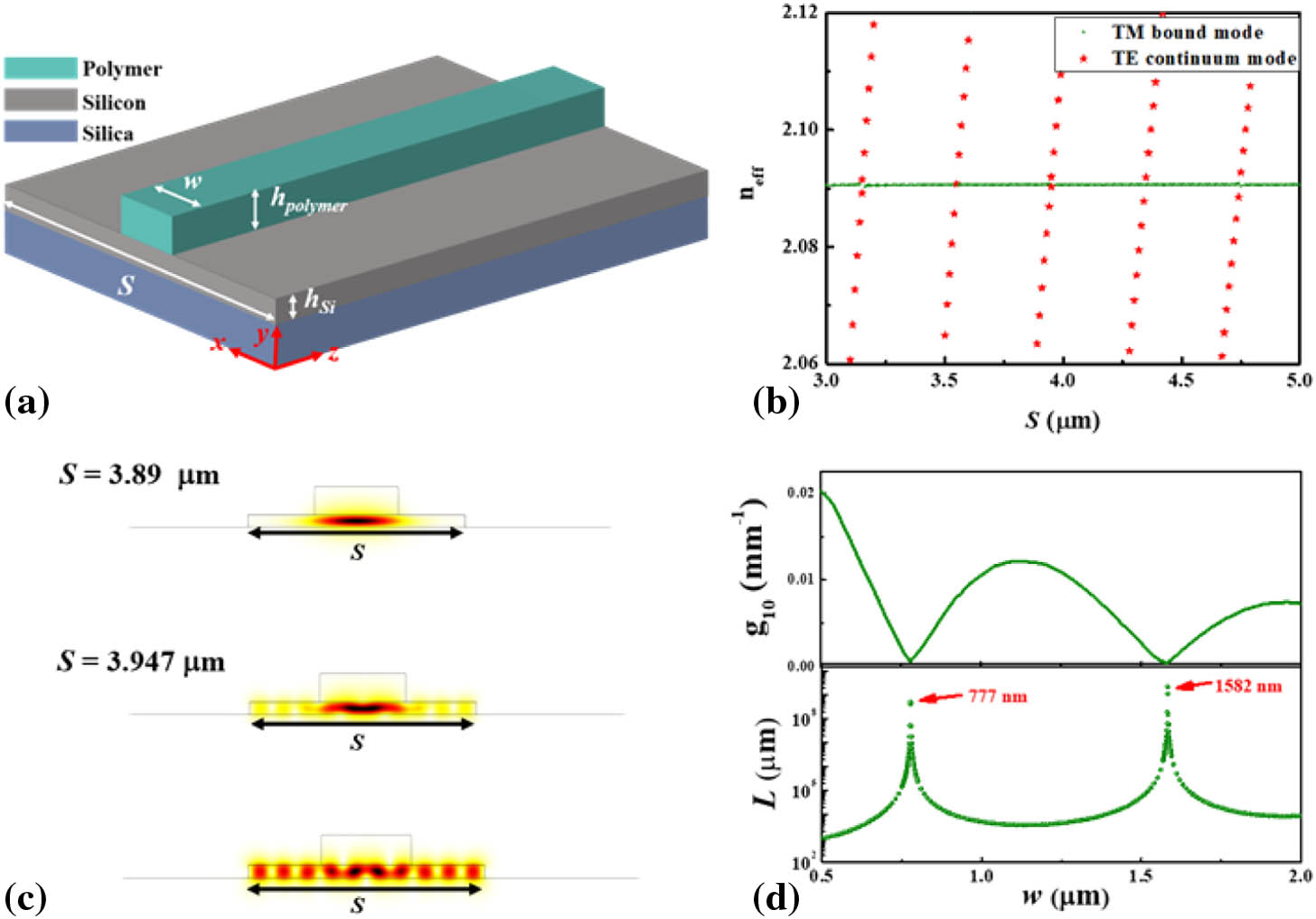
To better understand the working principle of the presented system, let us first review the properties of archetypical BIC waveguides. For simplicity, the working wavelength is focused on 1.55 μm. Figure 1(a) shows a conceptual schematic of a BIC waveguide, where a waveguide with low-refractive-index material (polymer, ) is patterned on a high-refractive-index substrate with a height (silicon, ). The height and width of the waveguide are defined as and , respectively. Here, the waveguide width related to the phase difference of the dissipation channels is the main factor that affects the formation of the BICs. We fix the waveguide height as 500 nm and tune the width to impel the system into BIC status. In addition, the thin silicon substrate can be seen as a film waveguide and the calculated effective index of its fundamental propagating mode is . To obtain the coupling strength between the TM (parallel to the substrate) bound modes of the waveguides and the TE (parallel to the substrate) continuum modes of the substrate, a substrate with finite width is considered to analyze the coupling process. The results are summarized in Fig. 1(b). The continuum modes are discretized as sequential orders under condition . is the wave vector component along direction [16], where is the effective index of the th continuum mode. The width of the polymer waveguide is chosen to be 1.5 μm as an example. The effective indices of continuum modes vary along with while the effective index of bound mode is constant. When the two modes are on resonance (), an anti-crossing behavior of effective indices is observed for even . Then strong coupling is achieved that makes the new eigenmodes exhibit hybridized field distributions of involved bound and continuum modes, as shown in Fig. 1(c).
Figure 1.Conventional BIC waveguide. (a) Schematic of the BIC waveguide. (b) Effective mode indices of the TM bound mode and the TE continuum modes with varying substrate width . (c) Field distributions under different . (d) Upper panel: solved coupling strength as a function of waveguide width . Lower panel: propagation distance at various waveguide widths with infinite . Red arrows indicate the maximum values.
We then define the effective index difference between two new eigenmodes as [16] where and is the coupling strength between the bound mode and the th continuum mode, respectively. Hence, if the coupling occurs, the coupling strength is nonzero. Then we have larger than zero when , which leads to the anti-crossing of the effective index trajectories, as shown in Fig. 1(b). It is obvious that reaches the minimum value at anti-crossing point (), and Eq. (1) is simplified as . For a structure with a finite substrate width , the coupling strength of the TM waveguide bound mode and TE propagating continuum modes reads [17] where represents the phase difference between loss channels [16] and is a constant that can be numerically obtained. In the case of infinite width , the coupling from the bound mode to the continuum modes leads to Markov system–environment interaction [26]. Then, the propagation length of bound mode can be expressed as with the density of the continuum modes . According to Eq. (3), the propagation length is written as the expression without and tends to infinite when . Therefore, the propagation characteristics of a BIC waveguides for infinite only depend on the coupling strength and mode density in the case of finite . Figure 1(d) shows the coupling strength as a function of the waveguide width . Based on numerically evaluated and Eq. (3), the propagation length can be obtained and there are maximum values for optimized where the bound mode is nearly decoupled from the continuum modes. Although a large range (0.5–2 μm) is chosen to search the photonic BICs, only two waveguide parameters [ and 1582 nm, see Fig. 1(d)] meet the BIC conditions (e.g., destructive interference). In this regard, the limited options of can be a pivotal factor that determines the performance of devices in some specific scenes such as the phase matching of coupling [27,28].
From the discussions above, important information can be extracted. The onset of losses from top waveguide bound mode to the substrate continuum state relies on whether or not destructive interference occurs. This crucial rule offers an opportunity to control the loss channels in additional ways. As shown in Fig. 2(a), an identical waveguide () is introduced next to the initial waveguide and the gap between them is set as . Due to the identical parameters of two waveguides, the phase-matching condition of their eigenmodes is spontaneously satisfied. Then an extra optical path introduced by waveguide interval should be considered, which opens a route to connect two waveguides through the coupling with TE continuum states. As depicted in Fig. 2(b), all the leakage channels from the TM waveguide bound modes to the TE continuum modes at the waveguides corners are plotted. () and () represent the left-going (right-going) leakage modes for the left waveguide, and () and () are left-going (right-going) leakage modes for the right waveguide, respectively.
Figure 2.BIC in dual waveguide configuration. (a) Schematic of BICs consists of two waveguides with interval . The widths are defined as and , respectively. (b) Loss channels formed by energy leaking from the TM bound mode to the TE continuum mode.
In such configuration, if the leakage channels and destructively interfere and cancel each other, the left-going loss component will eventually survive and dim the decay length. Likewise, the right-going component will be left simultaneously due to the symmetry of the structure. Consequently, the whole system will suffer heavy loss and hardly access the BIC status. As we are discussing the waveguide with an arbitrary width, () and () will not interfere and further shut down the leakage loss. Therefore, the conceivable way to establish BICs of this framework is that the phases of () and () satisfy the condition of destructive interference and extinguish the strong energy leakage. For the dual waveguide case, and according to the analysis of a single BIC waveguide, the phase difference of the left-going loss channel pairs () and () can be expressed as with . Similarly, the phase difference of the right-going leakage waves [ () and ()] holds the same expression. Based on Eq. (3) and for the purpose of driving the dual waveguide system to BIC status, the condition must be satisfied. To qualitatively confirm the analysis above, the value of is exactly calculated according to the phase difference between these leakage channels. It can be found that between and , clearly excluding the possibility of destructive interference of the two channels. As expected, is calculated to be for and , which matches the low-loss condition of the BICs. Then, we know that and are another pair of channels that interfere with each other due to the same phase difference as that of and . Likewise, it can be concluded that () and () satisfy the requirement of destructive interference because of the geometric symmetry of the system.
Here, to examine the discussion above and verify the exceptional role of the second waveguide, we take the waveguide widths μ as examples to construct BICs in such an architecture. All the results are summarized in Fig. 3. From Fig. 1(d), we know that the single waveguide with μ does not meet the condition for BICs; therefore, the introduction of the second waveguide should be the pivotal ingredient for the BICs that emerged in Fig. 3. Like the single waveguide situation, a clear coupling process can be seen between the TM bound mode and the TE continuum modes when the thin silicon substrate width is set to be finite, as shown in Fig. 3(a). Notably, a pair of TM bound modes are supported by the dual waveguide system; i.e., symmetric (olive circles) and antisymmetric modes (blue empty circles). It is seen that both of their mode index trajectories exhibit crossing and anti-crossing points but at different . This is because the parity of the symmetric mode is odd, which will couple with the continuum modes with an even order. In contrast, the antisymmetric mode’s parity is even, indicating the wave functions overlap between the antisymmetric mode and the odd order continuum modes. Both of them can reach the condition of BICs but at different waveguide intervals. Here, we choose a symmetric mode to explore the mechanism that accounts for the construction of the BICs. For the case of a symmetric mode, the crossing and anti-crossing behaviors appear periodically with the variation of . At the anti-crossing points, the new eigenmodes exhibit mixed field features of bound and continuum modes, as shown in Fig. 3(b). Moreover, the coupling strength can be further calculated by extracting the difference of the minimum effective indices at the anti-crossing points. Note that a few dips around 0 are obtained by tuning the gap for finite width , distinctly demonstrating the decoupling between the bound mode and the continuum mode. Then the propagation length is obtained under different leveraging on Eq. (3) and features peak values where the losses are frozen, surprisingly confirming the formation of BICs in a dual waveguide system, as shown in the lower panel in Fig. 3(c). For the dual waveguide system illustrated in Fig. 2, the loss elimination originates from the destructive interference of leakage channels from two waveguides. Therefore, to obtain the interaction-induced interference, the two waveguides are externally excited simultaneously from left port, as shown in Fig. 3(d). The energy is equally distributed in two waveguides and propagates along the direction with nearly zero loss.
Figure 3.Numerically calculated coupling strength for dual BICs waveguides. (a) Effective indices of the symmetric TM bound modes (olive circles), antisymmetric TM bound modes (blue empty circles), and TE continuum modes (red stars) as a function of the silicon substrate width . (b) Electric field distributions of the modes marked in (a). (c) Coupling strength (upper panel) and propagation length (lower panel) against waveguide interval , respectively. (d) Electric field distribution of the dual waveguide system along propagation direction with μ and μ for infinite .
As discussed above, the total value of and becomes the deterministic factor to affect the phase difference. In this respect, for any waveguide width, we always can find a proper to acquire with the phase difference . To affirm this, different waveguide widths () are applied and the decay lengths are calculated correspondingly, as shown in Fig. 4. It is obvious that robust BICs are formed at each waveguide width with assertive interval , clearly verifying the feasibility of the proposed mechanism. The presented design provides an achievable manner to manipulate radiation channels in optical waveguides, which holds great potential for information transportation in photonic circuits and improves the fabrication tunability.
Figure 4.Propagation distance under varied waveguide gaps . The waveguide width from 1 to 1.5 μm is selected to explore the BICs established in the dual waveguide architecture.
The fabrication error in the implementation of a dual waveguide system is indeed a crucial issue that is essential to consider. In this sense, improving the fabrication tolerance is an effective way to boost practical potential of the structure. As shown in Fig. 5(a), a cladding layer is introduced to reach this goal. Here, we still take μ as an example and define as the width range where the propagation length is larger than μ. When the refractive index of the cladding layer changes from 1 to 1.45, it is seen that the value of is gradually enlarged with the increase of . For (i.e., the air in Fig. 3), is around 20 nm, which is a challenging task for standard micro/nano fabrication technology. Surprisingly, is visibly improved and even reaches 80 nm at (such as ), which is almost four times larger than that for . In this situation, the fabrication tolerance is significantly improved, and the fabrication error is acceptable for the practical realization of the dual waveguide system. In addition, the cladding layer can be readily deposited by sputtering or E-beam evaporation. Furthermore, to investigate the physics behind the cladding layer induced broadening of width range , we have calculated the coupling strength of the 14th continuum mode for , as summarized in Fig. 6(a). In this case, the coupling strength shows a minimum value () near , indicating the occurrence of BIC. Due to the introduction of the cladding layer, the mode field overlap of the bound mode and continuum mode decreases. In this sense, it is seen that the coupling strength for is almost one order of magnitude lower than that for in Fig. 3(c). Consequently, the variation trend becomes slow and thus the curve envelope is broadened. According to Eq. (3), the width range is, therefore, effectively improved, as shown in Fig. 5(f).
Figure 5.Cladding-layer-covered dual waveguide system. (a) Schematic of the dual waveguide system with a cladding layer. (b)–(f) Propagation length as a function of waveguide intervals with , 1.2, 1.3, 1.4, and 1.45, respectively. The width range between black arrows is defined as . (g) Width range against .
Figure 6.BIC in dual waveguide system with cladding layer. (a) Coupling strength against waveguide interval . Here, the waveguide width is μ and . (b) Tendency of propagation length with the width of the dual waveguide system. Here, is fixed as 1.1 μm.
Besides the waveguide intervals , another issue of concern is the waveguide width difference between two waveguides in the practical fabrication. Here, we also analyzed the tendency of the propagation length with the width of the waveguide for the dual waveguide system based on the introduced cladding layer. As shown in Fig. 6(b), the width is fixed at 1.1 μm, while the waveguide width varies from 1 to 1.2 μm. It is clearly seen that the propagation length still exceeds μ with the waveguide width difference , obviously confirming the momentous and effective role of the cladding layer and the relatively high fabrication tolerance of the system. Notably, the proposed cladding layer strategy also works in the case of a single BIC waveguide, and the width range is improved from 20 nm [see Fig. 1(d)] to . The corresponding discussions are summarized in Appendix A.
3. CONCLUSION
In conclusion, we have proposed a dual waveguide system to remove the limitation to obtain BICs in a single waveguide configuration. According to our analysis, the phase difference of the leakage channels is determined by the total value of the waveguide width and interval . In this sense, the BIC conditions [destructive inference with ] can be satisfied at each waveguide width when the appropriate waveguide interval is chosen. Moreover, considering the practical fabrication of the presented system, a cladding layer with is introduced to improve the fabrication tolerance of the structure. The width range where the propagation length μ is optimized from 20 to 80 nm when is set to be 1.45 (corresponding to the refractive index of ), significantly enhancing the feasibility of the proposed mechanism. The findings in this work offer an alternative solution to construct BICs and may be helpful to improve the potential of BIC photonic devices and circuits.
APPENDIX A: THE FABRICATION TOLERANCE AT DIFFERENT WAVEGUIDE WIDTHS
When the cladding layer is introduced into the dual waveguide system, the fabrication tolerance is distinctly ameliorated. Our numerical calculations show that such improvement is applicable for other waveguide widths. As confirmed in Fig. 7, the values of can be optimized with the increase of at μ, 1.3 μm, and 1.4 μm, undoubtedly verifying the generality of the cladding layer strategy. Moreover, the proposed cladding layer strategy also functions well for the cases of a single waveguide structure in Fig. 1. Leveraging on the cladding layer with covered onto the waveguide, the is visibly broadened from 20 to 100 nm, clearly proving the effective and exceptional role of cladding layer in BIC waveguide configurations.
Figure 7.Fabrication tolerance of (a) the dual waveguide system and (b) the single waveguide system.