1State Key Laboratory of Advanced Optical Communication Systems and Networks, Shanghai Key Laboratory of Navigation and Location Services, Department of Electronic Engineering, Shanghai Jiao Tong University, Shanghai 200240, China
2SJTU-Pinghu Institute of Intelligent Optoelectronics, Pinghu 314200, China
On-chip Fourier-transform spectrometers (FTSs) based on Mach–Zehnder interferometer (MZI) arrays suffer from severe central wavelength and fringe contrast variation due to fabrication errors. Even though a calibration matrix can be employed to correctly retrieve the input spectra, environmental temperature variation greatly degrades the retrieving performance. In this paper, we devise a dual-layer waveguide interferometer to reduce the temperature sensitivity. The beating of the even and odd supermodes in the dual-layer waveguide generates periodic intensity fluctuations in the spectrum. Since these two modes have similar modal profiles, their thermal sensitivity and propagation loss are relatively balanced, leading to a low temperature sensitivity and a high interference extinction ratio. We designed and fabricated a passive FTS based on a 32-channel dual-layer waveguide array. Experimental results show that the temperature sensitivity is reduced to 10 pm/°C, which is almost half that of single-layer MZI-based FTSs. With this chip, we accurately reconstructed various types of optical spectra, including single and two sparse laser lines, and broadband optical spectra. Our method can fit a wide wavelength range, which is a promising technology to improve the practical applications of on-chip FTSs.
1. INTRODUCTION
Miniaturized optical spectrometers have wide applications, such as spectroscopic sensing, optical network performance monitoring, hyperspectral imaging, and radio frequency spectrum analysis, and offer dramatic size, weight, and power reductions [1–3]. Among various types of miniaturized optical spectrometers, on-chip Fourier-transform spectrometers (FTSs), which use interferometers to modulate the input light to generate interferograms, and retrieve the spectrum via the Fourier transform, are regarded as a promising technology for high-resolution, compact optical spectrometers. With the intrinsic advantages of silicon photonics, silicon-based FTSs can further reduce the device size as well as the cost, due to their high index contrast and CMOS compatibility. Recently, various on-chip FTSs have been demonstrated based on a Mach–Zehnder interferometer (MZI) array with various optical path differences (OPDs) [4–8], which is one of the most common optical components used in photonic integration. The MZI array modulates the input light into spatially distributed interferograms, which are analogous to conventional Michelson interferometer-type FTSs. The resolution can be enhanced either by increasing the OPDs or by using advanced spectral retrieving algorithms, like compressive sensing and machine learning [9–12]. Besides the communications band, on-chip FTSs have also been demonstrated for the mid-IR band [13–16]. Some of the works are also focused on approaches to improve the tunability or the scalability of MZIs to get a higher spectral resolution. For example, with cascaded optical switches to reconfigure the MZI arm length, the OPD can be digitally tuned to realize high-resolution scalable FTSs [17–19]. Upon thermo-optic or electro-optic modulation of one of the MZI arms, the OPD can also be continuously tuned and, in this case, it only needs one MZI to realize the FTS [20–22].
Conventionally, due to fabrication errors, the central wavelength and the fringe contrast of FTSs deviate from the design. Therefore, a calibration matrix is required to retrieve the input spectrum. The accuracy of the calibration matrix determines the correctness of the retrieved spectrum. However, silicon has a relatively large thermo-optic coefficient (TOC), which makes silicon photonic devices sensitive to environmental temperatures. Typically, the thermal sensitivity is about 100 pm/K. The environmental temperature variation in the calibration and the spectrum measurement results in deviation of the retrieved spectrum. It greatly limits the practical usage of such on-chip FTSs, especially when the resolution is very high. One way to reduce the temperature sensitivity is to use asymmetric MZIs with different arm widths and lengths to cancel the temperature-dependent phase difference between the two MZI arms [23–25]. However, the temperature-insensitive operation bandwidth is very narrow. A subwavelength grating (SWG) structure can engineer the dispersion of the waveguide, and thus can enhance the operation bandwidth [26]. However, it typically requires high-resolution electron beam lithography (EBL) to pattern the subwavelength gratings. Another way is to use negative TOC material as the waveguide upper cladding to cancel the positive TOC of the silicon waveguide core [27–29]. All the above methods need precise waveguide dimension control to eliminate temperature-induced degradation.
The second issue is the visibility of the interferogram. Typically, the extinction ratio (ER) of an asymmetric MZI is dependent on the power-splitting uniformity of the 3 dB couplers and the loss difference between the two arms. It is possible to realize high-performance, 3 dB couplers with both low power imbalance and a broad bandwidth based on an adiabatic design [30,31]. However, as the OPD of the MZI increases, the transmission loss difference between the two arms inevitably increases due to fabrication imperfection. As a result, the ER of the MZI decreases with the OPD. The reduced fringe visibility degrades the dynamic range of the spectral measurement.
Sign up for Photonics Research TOC. Get the latest issue of Photonics Research delivered right to you!Sign up now
Here, we propose and demonstrate what we believe, to the best of our knowledge, is a novel FTS based on a dual-layer spiral waveguide array. Two supermodes with different group indices are excited and interfere in the dual-layer waveguides, generating periodic spectral fringes. The TOC and propagation loss of the two supermodes are similar. Therefore, the temperature sensitivity and the ER of the waveguide interferometric structure are improved. With our chip, we successfully recover various types of input spectra, including single/dual separate laser lines and a broad optical signal.
2. DEVICE STRUCTURE AND WORKING PRINCIPLE
A. Dual-Layer Waveguide Interferometers
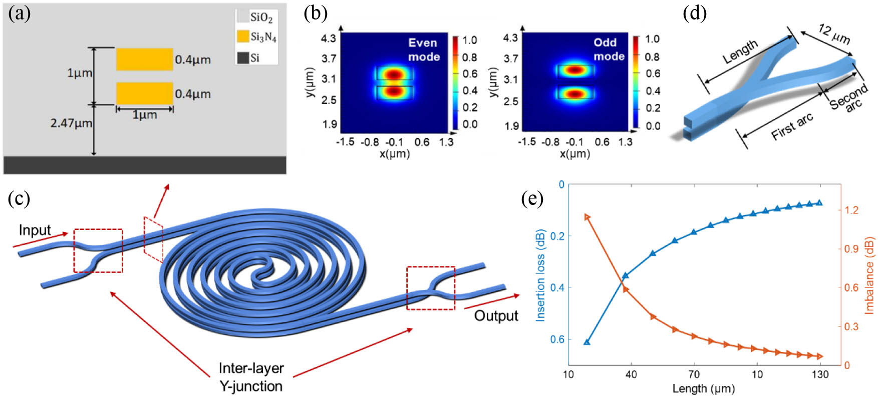
Figure 1(a) shows the cross-sectional view of the dual-layer waveguide. Two layers of silicon nitride waveguides with the same dimensions () are stacked vertically with a separation gap of 200 nm. Figure 1(b) presents the simulated electric field intensity profiles (TE polarization) of the even and odd supermodes of the dual-layer waveguide. The dual-layer waveguide can be regarded as a vertically coupled directional coupler (DC). Planar DCs have been widely used as power splitters. As we know, the working principle of a DC can be understood as the beating of even and odd supermodes in the composite waveguide, leading to optical intensity oscillation along the propagation direction. The beating length is inversely proportional to the difference of the propagation constants (or the effective indices) of the two supermodes. Conventionally, power splitters must process a large operational bandwidth. However, in our device, we use its interference effect to discriminate the frequency component of an input signal; therefore, its length is much longer than the crossing-coupling length so that a dense periodic interference spectrum results.
Figure 1.(a) Cross-section of the dual-layer waveguide. (b) Electric field intensity distribution of the even and odd supermodes of the dual-layer waveguide. (c) Schematic of the spiral-shaped dual-layer waveguide interferometer. (d) Schematic structure of the interlayer Y junction. (e) Simulated insertion loss and power imbalance of the interlayer Y junction under various lengths.
This periodic spectral response of the DCs is beneficial for the FTS application. The two supermodes have different group indices of and , and the OPD of the dual-layer waveguide structure is given by , where is the waveguide length. Hence, the free spectral range (FSR) is , where is the central wavelength of the input light in the vacuum. The group index difference between the two supermodes can be optimized by the waveguide geometry of the dual-layer waveguide. The FSR of the interference is related to the FTS resolution and the operation bandwidth.
To excite and split these two supermodes, we added two interlayer Y junctions at the input and output ends of the dual-layer waveguide. Figure 1(c) presents the schematic structure of the holistic dual-layer waveguide interferometer. The dual-layer waveguide is arranged in a spiral shape to reduce the chip footprint. This is the advantage of dual-layer waveguides over planar DCs. Light from the upper (bottom) branch of the input interlayer Y junction can be evenly split into the even and odd supermodes at the junction. The interference of the two supermodes in the dual-layer waveguide results in the optical intensity oscillation along the propagation direction. At the output interlayer Y junction, the optical power in the two layers is divided. Therefore, the detected power from either single-layer waveguide is oscillatory with respect to the wavelength. The interlayer Y junction works as a 3 dB coupler and the entire dual-layer waveguide interferometer resembles an asymmetric MZI commonly used in FTS chips.
Figure 1(d) shows the structure of the interlayer Y junction, which is formed by two layers. The Y junction is simply designed with two arcs in both the upper and lower branches. Typically, the junction part should be carefully designed to realize adiabatic mode evolution. However, in our design, we only set the bending radius of the interlayer Y junctions as 60 μm, which results in a large power imbalance, and thus a reduced ER. Figure 1(e) shows the 3D finite-different time-domain (FDTD) simulation results of the interlayer Y junction. In the simulation, light is launched into the upper branch of the Y junction, so it splits into even and odd supermodes at the output port. We monitored the output transmission of these two supermodes. Since the first arc decides the splitting speed of the two branches, we just varied the bending radius of the first arc while fixing the bending radius of the second arc and the spacing of the two ports as 60 μm and 12 μm, respectively. By increasing the bending radius of the first arc, the loss in the mode evolution is reduced, but the length of the Y junction also increases accordingly. As shown in Fig. 1(e), the insertion loss is 0.61 dB for the Y junction length of 18.9 μm, which corresponds to the bending radius of 60 μm used in our chip. It can be reduced to 0.07 dB when the length of the Y junction increases to 130 μm. The power imbalance is defined as the power ratio of these two supermodes in decibels. It can also be improved from 1.15 dB to 0.07 dB by increasing the length of the Y junction. To further reduce the length of the Y junction, we can optimize the shape of the arc by using the particle swarm optimization (PSO) method [32].
B. Temperature Sensitivity and ER Analysis
The temperature sensitivity of a conventional single-layer MZI can be expressed as the wavelength shift upon temperature variation, which is given by [33,34]where and are the TOC and the group index of the waveguide. The TOC of a waveguide can be expressed as [29]where and are the confinement factor and the material TOC. The thermal sensitivity of the single-layer MZI is highly dependent on the waveguide’s TOC. By using instead of Si as the waveguide core, the thermal sensitivity can be reduced because of the lower TOC as well as its lower mode confinement. For our dual-layer waveguide interferometer, the temperature sensitivity can be revised as where is the difference of the TOC of the odd mode () and the even mode (). The TOC difference relates to the temperature-dependent phase difference of the dual-layer waveguide structure. As can be seen in Fig. 1(c), the confinement factors in the core of the two supermodes are very close, which means the TOC difference is very small. By proper dimension design of the dual-layer waveguide, the confinement factors of the two supermodes can be identical; thus, the temperature sensitivity of the structure can be completely canceled.
Figure 2(a) shows the simulated group index difference and temperature sensitivity of the dual-layer waveguide under different waveguide widths and separation gaps at a wavelength of 1.56 μm. In the simulation, the TOC values of and are set as and , and the refractive indices of and are 1.99 and 1.444, respectively. The group index is calculated based on the finite difference eigenmode (FDE) method by the Ansys Lumerical MODE solution, and is calculated as . The waveguide TOC is calculated by Eq. (2), and the confinement factor is calculated based on Ref. [35]. In comparison, Fig. 2(b) shows the simulated group index and temperature sensitivity of the single-layer MZI. For the regular MZI structure based on single-layer waveguides, the temperature sensitivity slightly increases with the waveguide width because more light is confined in the . The temperature sensitivity is for a waveguide width of 1 μm. In contrast, with an increase in the waveguide width, the temperature sensitivity of the dual-layer waveguide interferometer changes from negative to positive and reaches the temperature-insensitive point with a proper waveguide width. In addition, as the separation gap increases from 0.2 to 0.3 μm, the temperature-insensitive waveguide width decreases accordingly. In this work, we chose the separation gap as 0.2 μm to be compatible with other designs in this multilayer -on-SOI (silicon on insulator) platform [36,37]. The absolute value of of the dual-layer waveguide increases with the waveguide width and is almost stable when the waveguide width is larger than 1.4 μm. Since the group index difference at the temperature-insensitivity point is relatively small, as illustrated by the orange dashed line in Fig. 2(a), we choose a width of 1 μm to balance the chip size and the temperature sensitivity of our FTS chip. The temperature sensitivity is . The temperature response can be flexibly tailored by the waveguide geometry of the dual-layer waveguide. Since is transparent over a wide wavelength range, it is also easy to extend the operation wavelength using the dual-layer waveguide structure.
Figure 2.(a) Group index difference and temperature sensitivity of the dual-layer waveguide when the separation gap changes from 0.2 to 0.3 μm. (b) Group index and temperature sensitivity of the single-layer MZI. (c) Extinction ratio of the two interferometer structures as a function of the FSR.
Besides the thermal stability, the contrast of the interference fringes is also very important for the accurate reconstruction of the input spectrum. However, as the OPD of the MZI increases, the length difference between the two arms increases, which increases the loss difference and degrades the ER. As for our dual-layer waveguide interferometer, the propagation length of the two interference modes is equal. Since the mode profiles of these two modes are similar, the loss difference between these two modes is greatly suppressed. Higher fringe contrast can be achieved with our waveguide structure. Figure 2(c) shows the simulated ERs of our dual-layer waveguide interferometer and the single-layer MZI structure under different FSRs. In the simulation, the extinction coefficient of is set to be , corresponding to a 1.026 dB/cm loss for a single-layer waveguide, and 1.059 dB/cm and 1.066 dB/cm for the even and odd modes of the dual-layer waveguide. The 3 dB coupler is considered as perfectly 50:50. We can see that even though the required length of the dual-layer waveguide is longer than that of an MZI for the same FSR, the ER of the dual-layer waveguide is almost 20 dB larger than that of the regular MZI. Therefore, it reveals that dual-layer waveguide structures also have better performance in fringe contrast.
C. FTS Chip Design and Fabrication
To demonstrate its performance, we designed a passive FTS chip consisting of a 32-channel dual-layer waveguide interferometer array with a linearly increased waveguide length. The input light is evenly split into 32 channels by five stages of power splitters. The power splitters are based on multimode interference (MMI) structures and implemented in the upper layer. The outputs of the MMI power splitters are connected to the upper input ports of the interlayer Y junctions to evenly excite the even and odd supermodes in the dual-layer waveguide. The minimum length of the dual-layer waveguides is 1200 μm, and the length is increased with a step of 1200 μm. Therefore, the optical bandwidth is 7.67 nm and the spectral resolution is 0.48 nm. To reduce the footprint, these waveguides are designed in a spiral shape with a minimum bending radius of 60 μm, as shown in Fig. 1(c). The bending radius can be further reduced using an Euler-bend design [38]. At the output port of each spiral waveguide, another interlayer Y junction converts the modes of the dual-layer waveguide into two separated modes in the upper and the bottom layers. The upper-layer waveguides are used for optical power measurement. The other ports of the Y junctions are routed to silicon grating couplers by interlayer couplers, which are used as test ports.
The fabrication of the chip starts from an 8-inch SOI wafer with a 220 nm thick top silicon layer and 3 μm thick bottom oxide layer. The layers were deposited by low-pressure chemical vapor deposition (LPCVD) and flattened by chemical–mechanical polishing (CMP). The silicon and the waveguides were patterned by 248 nm deep UV (DUV) lithography followed by dry etching. The whole chip was fabricated by the Shanghai Industrial μTechnology Research Institute (SITRI). Figure 3(a) shows the microscope image of the fabricated chip. The footprint of the chip is . Figure 3(b) shows the SEM image of the dual-layer waveguide. The etched waveguide angle is about 82°. Input and output fiber couplers are based on inverse tapers with a tip width of 200 nm, all arranged on the left edge of the chip. Two U-shaped bending waveguides are used to assist the coupling with a 37-channel fiber array. The coupling loss is . Figure 3(c) shows the FTS chip after the optical package. The chip was packaged by SJTU-Pinghu Institute of Intelligent Optoelectronics.
Figure 3.(a) Microscope image of the fabricated chip. (b) SEM image of the dual-layer waveguide cross-section. (c) Picture of the packaged chip.
We characterized the thermal sensitivity of our dual-layer waveguide. For comparison, we also measured the thermal sensitivity of two microring resonators (MRRs) made of single-layer waveguides in the upper and bottom layers. The waveguide width is also 1 μm. Figures 4(a)–4(c) show the measured transmission spectra of these three test devices when the temperature increases from 20°C to 60°C. The extracted central wavelength shifts are shown in Figs. 4(d)–4(f). We can see that the thermal sensitivities of our dual-layer waveguide and the single-layer MRRs are and 17.8 pm/°C, respectively, which is consistent with the simulation. The temperature-dependent wavelength shift is one order lower than the Si waveguide, and almost half that of the single-layer waveguide, which verifies that our FTS chip has low temperature sensitivity.
Figure 4.(a)–(c) Measured transmission spectra and (d)–(f) extracted central wavelength shift under various temperatures. (a) and (d) Dual-layer spiral waveguide; (b) and (e) MRR in the upper layer; and (c) and (f) MRR in the bottom layer.
To correct the fabrication imperfection-induced deviation of the periodic fringes in the dual-layer waveguide arrays, a calibration matrix was needed for spectral reconstruction. We measured the transmission spectra of the 32 waveguide interferometers using a tunable laser scanned from 1554 to 1566 nm wavelength with a step of 10 pm. The input power was set to 0 dBm. A group of 32-channel power meters were used to record the optical power from the 32 output ports of the waveguide interferometer array. Note that since our chip has high temperature stability, we did not use a thermoelectric cooler (TEC) in both the calibration and the spectral interrogation. Figures 5(a) and 5(b) show the measured spectra of the dual-layer spiral waveguide interferometers with the shortest and the longest waveguide lengths of 1.2 mm and 38.4 mm, respectively. The FSR of the longest waveguide interferometer is . The ER difference is negligible for the two waveguide interferometers. However, as mentioned above, the unoptimized interlayer Y junctions result in a relatively large power imbalance of the two supermodes, lowering the ER to over the measured wavelength range.
Figure 5.(a) and (b) Measured transmission spectra of (a) the shortest and (b) the longest dual-layer spiral waveguide interferometers of the FTS chip. The pink-shaded areas illustrate the wavelength range for spectral reconstruction. (c) Normalized calibration matrix obtained by a tunable laser.
We used the spectra in the wavelength range from 1556.5 to 1563.5 nm to construct the calibration matrix, which is slightly smaller than the operation bandwidth of our chip. The size of the calibration matrix is , with each row representing the spectral response of each waveguide interferometer in the FTS chip. To improve the spectral reconstruction, the measured transmission spectra were normalized with the maximum power for each interferometer, which is expressed as where is the normalized calibration matrix. Figure 5(c) displays the normalized calibration matrix, with each row representing the spectrum of a dual-layer waveguide interferometer.
In the spectral reconstruction, the tunable laser was replaced by an unknown input optical signal. The measured output power by the power meter was also normalized as where is a column vector with 32 elements representing the normalized output power. The input unknown spectrum can be expressed as a column vector consisting of 701 elements. The reconstruction of the unknown spectrum is to solve the vector from
We applied the elastic- regularization regression algorithm to retrieve the spectra , which has been proven as a powerful algorithm for both sparse and broadband spectra [17]. The objective function of the elastic- is expressed as where (, 2, 3) is the hyperparameter for each penalty term. We solved the equation above with standard convex optimization tools [17].
C. Spectral Reconstruction Results
We first evaluated the reconstruction ability for sparse spectra with a single laser line and two separate laser lines. The sparse laser lines were generated by one or two tunable laser sources, and the input power was set to 0 dBm. Figure 6(a) shows the reconstructed spectra of the input single-line laser. The input light changes from 1559 to 1559.96 nm with a step of 0.08 nm. The wavelengths of all the spectral lines are accurately recovered by our FTS chip, and the amplitudes are close to 1, indicating the good reconstruction performance of our chip. Figures 6(b)–6(f) show the results of two laser lines when the wavelength spacing increases from 0.2 to 1 nm with a step of 0.2 nm. When the spacing is above 0.2 nm, the two lines are clearly distinguished from each other, and the retrieved wavelengths match with the results from a benchtop optical spectrum analyzer (AQ63700, Yokogawa Electric), as illustrated by the orange dashed lines. However, splitting peaks are observed in Fig. 6(b) when the spacing is 0.2 nm, due to the limited resolution of our FTS chip. There also are a few peaks in the retrieved spectrum around the 1560 nm wavelength, which influences the retrieved amplitude of the sparse signal. The limited ER of our FTS chip reduces the discrimination of the wavelength position and therefore generates several wavelength components near the central wavelengths. In the future, we can increase the ER of the FTS by increasing the bending radius of the interlayer Y junctions and further improving the spectral resolution by increasing the length of the dual-layer waveguides and the number of waveguides in the array.
Figure 6.(a) Reconstructed spectra of the single narrowband laser source. (b)–(f) Measured and reconstructed spectra of the two narrowband laser sources with a wavelength spacing of (b) 0.2 nm, (c) 0.4 nm, (d) 0.6 nm, (e) 0.8 nm, and (f) 1 nm. PSD, power spectral density.
We also characterized the reconstruction performance for broadband optical spectra. The input spectrum was generated using an amplified spontaneous emission (ASE) light source and a tunable optical bandpass filter. The bandwidth of the filter was tuned, and the bandwidth of the input optical signal varied from 1 to 4 nm. To better evaluate the reconstruction performance, we normalized both the retrieved spectra and the measured spectra to the maximum. Figure 7 shows the reconstructed results with our on-chip spectrometer. As observed, the reconstructed envelope shape fits the measured shape very well. The slant optical passbands are due to the ASE light source. The value calculated from the reconstructed and the measured spectra is close to 1, indicating good reconstruction performance.
Figure 7.Measured and reconstructed spectra of a broadband optical signal with the bandwidth increasing from 1 to 4 nm. PSD, power spectral density.
Finally, we implemented the spectral reconstruction for a single-line laser source at the 1560 nm wavelength and a broadband optical signal with a bandwidth of 1 nm under various temperatures. The temperature was adjusted by a TEC, and the calibration matrix was obtained at the initial temperature. The reconstruction algorithm was also based on the elastic- regularization method. Figure 8(a) shows the reconstruction results for a single-line laser source. We can see that with the increased temperature deviation, a shorter wavelength line rises from the reconstructed spectrum. When the temperature deviation reached 1.4°C, the amplitude of the shorter wavelength line was almost close to the original laser line. Since the calibration matrix is fixed, and the temperature variation causes a red shift of the output spectrum of the waveguide interferometers, the wavelength position of the recovered spectrum shifts to the blue side. Figure 8(b) shows the reconstructed spectra for the broadband optical signal. The central wavelength and the envelope of the reconstructed signal change slightly, even with a 10°C temperature variation. We used the value under various temperatures to determine the fidelity of the retrieved spectrum. When the temperature variation is less than 5°C, the value is larger than 0.9.
Figure 8.Reconstructed spectra of (a) the single-line laser source and (b) the broadband optical signal under various temperatures.
Table 1 compares our work to state-of-the-art passive FTS chips reported in the literature. Most of the previous works focused on the improvement of the resolution. However, because they are constructed using silicon-based asymmetric MZIs, they suffer from a high temperature sensitivity of about 100 pm/°C [6,7,12]. Using the temperature-dependent reconstruction algorithm can reduce the temperature sensitivity, but it is only suited for a relatively small temperature range [39]. The temperature sensitivity of our method based on dual-layer waveguide interferometers is one order smaller than that of the conventional silicon-based FTS chips. It has a similar temperature sensitivity, compared to the other two passive compensation methods, which use negative TOC polymer in the waveguide and SWG structure to reduce the thermal phase shift [26,27]. Note that our chip is fully CMOS-compatible and the fabrication does not need high-resolution e-beam lithography. Our chip has a lower resolution compared to others, which can be enhanced by increasing the length of the dual-layer waveguides. Although the smaller group index difference of our method requires a much longer waveguide length compared to conventional MZI structures, the ER degradation is much less with the increasing OPD, and its size is still much smaller than that of the benchtop FTSs.
Comparison of Several Low Temperature Sensitivity On-Chip Spectrometers
Reference
Technology
Bandwidth (nm)
Resolution (nm)
Footprint ()
Temperature Sensitivity (pm/°C)
[6]
Si-SWG based MZIs
0.78
0.05
24
a
[7]
Si MZIs
0.6
0.085
4.5
a
[12]
Si MZIs
0.432
0.027
–
a
[39]
Si MZIs, reconstruction algorithm
0.22
0.017
23
–
[27]
/SU-8 hybrid waveguide-based MZI
1
0.05
264
b
[26]c
Tailored-SWG based MZI
0.76
0.047
–
7.5
This work
Dual-layer waveguide
7
0.4
26.68
Estimated from the temperature sensitivity of common Si waveguides.
Calculated from Fig. 6 of Ref. [27].
All the results are based on simulation.
In this work, the FTS chip only consists of 32 waveguide interferometers, which eventually restricts the measurement points. The spectral resolution can be further improved by increasing the length of the dual-layer waveguides, and the measurement points can be improved by increasing the number of waveguide interferometers. The chip architecture in this work used a passive power splitter to divide input light before the interferometer array. This caused the degradation of the SNR, which limits the number of interferometers. We can further improve our chip by using a tunable power splitter to replace the passive splitters or by designing a wide-area, grating-based light collection system to increase the input aperture [7]. We also can add an optical tunable filter before our FTS chip [21]. The passive FTS only retrieves a small portion of the input spectrum filtered by the optical tunable filter. By tuning the central wavelength of the filter, the whole spectrum can be reconstructed, which can greatly reduce the chip’s footprint.
In summary, we have demonstrated a low temperature sensitive FTS chip based on a dual-layer spiral waveguide array. The beating of the even and odd supermodes in the dual-layer waveguide generates periodic fringes in the transmission spectrum. Since these two supermodes have similar modal profiles, they have a very close TOC and transmission loss, in favor of a low temperature sensitivity and a high interference ER. The measured temperature sensitivity of our chip is , which is one order lower than that of the Si waveguide and almost half that of the single-layer waveguide. Using such an FTS chip, we successfully reconstructed various optical spectra, including sparse laser lines and broadband optical signals, with a minimum wavelength spacing of 0.4 nm and a wavelength range of 7 nm. Since has a wide transparent wavelength range, it is possible to realize temperature-insensitive on-chip FTSs with the dual-layer waveguide interferometers over a wide wavelength range.
Acknowledgment
Acknowledgment. The authors thank Shanghai Industrial μTechnology Research Institute (SITRI) for the chip fabrication and SJTU-Pinghu Institute of Intelligent Optoelectronics for the chip package.
[17] D. M. Kita, B. Miranda, D. Favela, D. Bono, J. Michon, H. Lin, T. Gu, J. Hu. High-performance and scalable on-chip digital Fourier transform spectroscopy. Nat. Commun., 9, 4405(2018).
[36] W. Gao, X. Li, L. J. Lu, J. P. Chen, L. J. Zhou. Broadband, low-crosstalk and power-efficient 32x32 optical switch on a dual-layer Si3N4-on-SOI platform. Optical Fiber Communication Conference (OFC), W4B.4(2022).